Intersil Corporation HPLR3103, HPLU3103 Datasheet

HPLR3103, HPLU3103
Data Sheet July 1999 File Number
52A, 30V, 0.019 Ohm, N-Channel Logic
Level, Power MOSFETs
These are N-Channel enhancement mode silicon gate
power field effect transistors. They are advanced power
MOSFETs designed, tested, and guaranteed to withstand a
specified level of energy in the breakdown avalanche mode
of operation. All of these power MOSFETs are designed for
applications such as switching regulators, switching
converters, motor drivers, relay drivers, and drivers for high
power bipolar switching transistors requiring high speed and
low gate drive power. These types can be operated directly
from integrated circuits.
Ordering Information
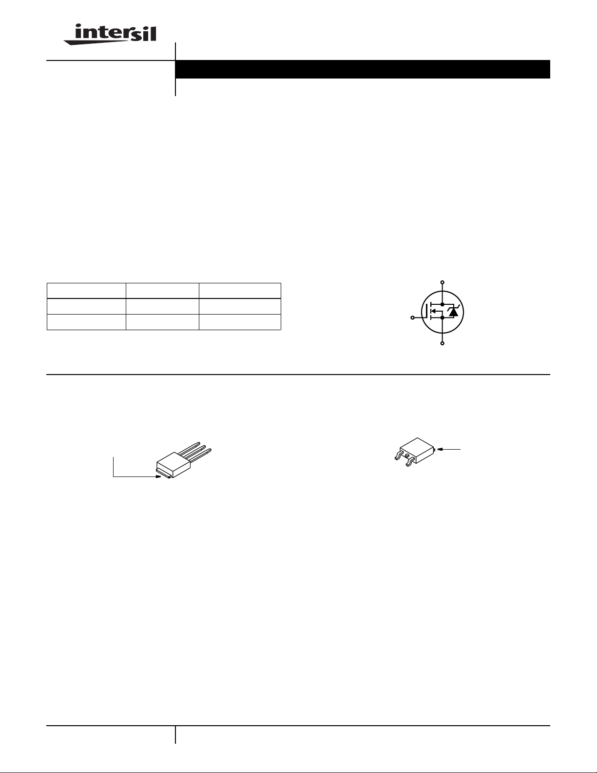
PART NUMBER PACKAGE BRAND
HPLU3103 TO-251AA HP3103
HPLR3103 TO-252AA HP3103
NOTE: Whenordering, use the entire part number.AddthesuffixT
to obtain the TO-252AA variant in tape and reel, e.g., HPLR3103T.
4501.2
Features
• Logic Level Gate Drive
• 52A†, 30V
• Low On-Resistance, r
DS(ON)
= 0.019Ω
• UIS Rating Curve
• Related Literature
- TB334, “Guidelines for Soldering Surface Mount
Components to PC Boards”
Calculated continuous current based on maximum allowable junction
†
temperature. Package limited to 20A continuous, see Figure 9.
Symbol
D
G
S
Packaging
(FLANGE)
JEDEC TO-251AA JEDEC TO-252AA
DRAIN
SOURCE
DRAIN
GATE
GATE
SOURCE
DRAIN
(FLANGE)
6-3
CAUTION: These devices are sensitive to electrostatic discharge; follow proper ESD Handling Procedures.
http://www.intersil.com or 407-727-9207
| Copyright © Intersil Corporation 1999

HPLR3103, HPLU3103
Absolute Maximum Ratings T
= 25oC, Unless Othewise Specified
C
HPLR3103, HPLU3103 UNITS
Drain to Source Voltage (Note 1). . . . . . . . . . . . . . . . . . . . . . . . . . . . . . . . . . . . . . . . . . V
Drain to Gate Voltage (RGS = 20kΩ) (Note 1) . . . . . . . . . . . . . . . . . . . . . . . . . . . . . . .V
Gate to Source Voltage . . . . . . . . . . . . . . . . . . . . . . . . . . . . . . . . . . . . . . . . . . . . . . . . . . V
Continuous Drain Current . . . . . . . . . . . . . . . . . . . . . . . . . . . . . . . . . . . . . . . . . . . . . . . . . . I
Pulsed Drain Current (Note 2) . . . . . . . . . . . . . . . . . . . . . . . . . . . . . . . . . . . . . . . . . . . . . .I
Single Pulse Avalanche Energy (Note 4). . . . . . . . . . . . . . . . . . . . . . . . . . . . . . . . . . . . . E
Power Dissipation . . . . . . . . . . . . . . . . . . . . . . . . . . . . . . . . . . . . . . . . . . . . . . . . . . . . . . . P
DSS
DGR
GS
D
DM
AS
D
Derate Above 25oC . . . . . . . . . . . . . . . . . . . . . . . . . . . . . . . . . . . . . . . . . . . . . . . . . . . . . . .
Operating and Storage Temperature . . . . . . . . . . . . . . . . . . . . . . . . . . . . . . . . . . . . TJ, T
STG
Maximum Temperature for Soldering
Leads at 0.063in (1.6mm) from Case for 10s. . . . . . . . . . . . . . . . . . . . . . . . . . . . . . . . . .T
Package Body for 10s, See Techbrief 334 . . . . . . . . . . . . . . . . . . . . . . . . . . . . . . . . . . T
CAUTION: Stresses above those listed in “Absolute Maximum Ratings” may cause permanent damage to the device. This is a stress only rating and operationofthe
device at these or any other conditions above those indicated in the operational sections of this specification is not implied.
L
pkg
30 V
30 V
±16V V
52
390
240 mj
89
0.71
-55 to 150
300
260
A
A
W
W/oC
o
C
o
C
o
C
NOTE:
1. TJ = 25oC to 125oC.
Electrical Specifications T
= 25oC, Unless Otherwise Specified
C
PARAMETER SYMBOL TEST CONDITIONS MIN TYP MAX UNITS
Drain to Source Breakdown Voltage BV
Gate to Source Threshold Voltage V
Zero Gate Voltage Drain Current I
DSSID
GS(TH)VGS
DSS
= 250µA, VGS = 0V 30 - - V
= VDS, ID = 250µA1--V
VDS = 30V, VGS = 0V - - 25 µA
VDS = 24V, VGS = 0V, TC = 125oC - - 250 µA
Gate to Source Leakage Current I
Breakdown Voltage Temperature
Coefficient
Drain to Source On Resistance
∆V
(BR)DSS
/∆T
r
DS(ON)ID
(Note 3)
Turn-On Delay Time t
d(ON)
Rise Time t
Turn-Off Delay Time (Note 3) t
d(OFF)
Fall Time t
Total Gate Charge Q
Gate to Source Charge Q
Gate to Drain “Miller” Charge Q
Input Capacitance C
Output Capacitance C
Reverse Transfer Capacitance C
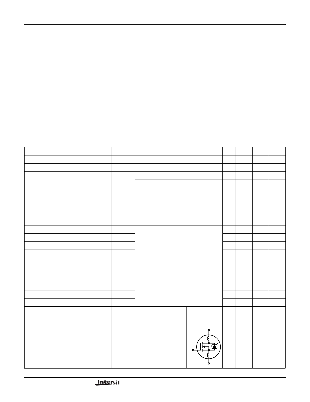
Internal Source Inductance L
Internal Drain Inductance L
GSS
OSS
RSS
VGS = ±16V - - 100 nA
Reference to 25oC, ID = 1mA - 0.037 - V
J
= 28A, VGS = 10V - - 0.019 Ω
ID = 23A, VGS = 4.5V - - 0.024 Ω
VDD= 15V, ID≅34A, RL= 0.441Ω,VGS=4.5V,
RGS =3.4Ω, I
r
g(REF)
= 3mA
-9 - ns
- 210 - ns
-20 - ns
f
VDD = 24V
g
ID≅ 34A,
gs
VGS = 4.5V
(Figure 6)
gd
VDS = 25V, VGS = 0V,
ISS
f = 1MHz (Figure 5)
-54 - ns
- - 50 nC
- - 14 nC
- - 28 nC
- 1600 - pF
- 640 - pF
- 320 - pF
Measured From the
S
SourceLead,6mm(0.25in)
FromPackage toCenter of
Die
Measured From the Drain-
D
Lead, 6mm (0.25in) From
ModifiedMOSFET
Symbol Showing
the Internal Devices Inductances
D
L
D
- 7.5 - nH
- 4.5 - nH
Package to Center of Die
G
L
S
S
6-4
 Loading...