

HP4936DY
Data Sheet August 1999 File Number
5.8A, 30V, 0.037 Ohm, Dual N-Channel,
Logic Level Power MOSFET
This power MOSFET is manufactured using an innovative
process. This advanced process technology achieves the
lowest possible on-resistance per silicon area, resulting in
outstanding performance. This device is capable of
withstanding high energy in the avalanche mode and the
diode exhibits very low reverse recovery time and stored
charge. It was designed for use in applications where power
efficiency is important, such as switching regulators,
switching converters, motor drivers, relay drivers, lowvoltage bus switches, and power management in portable
and battery-operated products.
Ordering Information
PART NUMBER PACKAGE BRAND
HP4936DY SO-8 P4936DY
NOTE: When ordering, use the entire part number.Add the suffix T
to obtain the variant in tape and reel, e.g., HP4936DYT.
Features
• Logic Level Gate Drive
• 5.8A, 30V
•r
•r
• Related Literature
- TB334, “Guidelines for Soldering Surface Mount
= 0.037Ω at ID = 5.8A, VGS = 10V
DS(ON)
= 0.055Ω at ID = 4.7A, VGS = 4.5V
DS(ON)
Components to PC Boards”
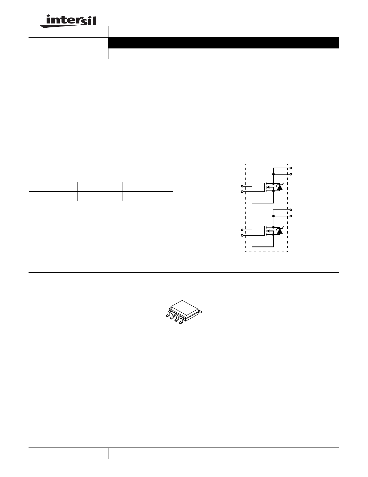
Symbol
D1(8)
D1(7)
S1(1)
G1(2)
D2(6)
D2(5)
4469.3
Packaging
S2(3)
G2(4)
SO-8
8-8
CAUTION: These devices are sensitive to electrostatic discharge; follow proper ESD Handling Procedures.
http://www.intersil.com or 407-727-9207
| Copyright © Intersil Corporation 1999
HP4936DY
Absolute Maximum Ratings T
= 25oC, Unless Otherwise Specified
A
HP4936DY UNITS
Drain to Source Voltage (Note 1). . . . . . . . . . . . . . . . . . . . . . . . . . . . . . . . . . . . . . . . . . V
Drain to Gate Voltage (RGS = 20kΩ) (Note 1) . . . . . . . . . . . . . . . . . . . . . . . . . . . . . . . . V
Gate to Source Voltage . . . . . . . . . . . . . . . . . . . . . . . . . . . . . . . . . . . . . . . . . . . . . . . . . . V
DSS
DGR
GS
30 V
30 V
±16 V
Drain Current
Continuous. . . . . . . . . . . . . . . . . . . . . . . . . . . . . . . . . . . . . . . . . . . . . . . . . . . . . . . . . . . .I
Pulsed Drain Current (10µs Pulse Width) . . . . . . . . . . . . . . . . . . . . . . . . . . . . . . . . . . .I
Power Dissipation . . . . . . . . . . . . . . . . . . . . . . . . . . . . . . . . . . . . . . . . . . . . . . . . . . . . . . . P
D
DM
D
Derate Above 25oC . . . . . . . . . . . . . . . . . . . . . . . . . . . . . . . . . . . . . . . . . . . . . . . . . . . . . . .
Operating and Storage Temperature . . . . . . . . . . . . . . . . . . . . . . . . . . . . . . . . . . . . TJ, T
STG
Maximum Temperature for Soldering
Leads at 0.063in (1.6mm) from Case for 10s. . . . . . . . . . . . . . . . . . . . . . . . . . . . . . . . . .T
Package Body for 10s, See Techbrief 334 . . . . . . . . . . . . . . . . . . . . . . . . . . . . . . . . . . T
CAUTION: Stresses above those listed in “Absolute Maximum Ratings” may cause permanent damage to the device. This is a stress only rating and operationofthe
device at these or any other conditions above those indicated in the operational sections of this specification is not implied.
L
pkg
5.8
30
2
0.02
-55 to 150
300
260
A
A
W
W/oC
o
C
o
C
o
C
NOTE:
1. TA = 25oC to 125oC.
Electrical Specifications T
= 25oC, Unless Otherwise Specified
A
PARAMETER SYMBOL TEST CONDITIONS MIN TYP MAX UNITS
Drain to Source Breakdown Voltage BV
Gate to Source Threshold Voltage V
Zero Gate Voltage Drain Current I
DSSID
GS(TH)VGS
DSS
= 250µA, VGS = 0V 30 - - V
= VDS, ID = 250µA (Figure 9) 1 - - V
VDS = 30V, VGS = 0V - - 1 µA
VDS = 30V, VGS = 0V, TA = 55oC--25µA
Gate to Source Leakage Current I
Drain to Source On Resistance r
GSS
DS(ON)ID
VGS = ±16V - - 100 nA
= 4.7A, VGS = 4.5V (Figures 6, 8) - 0.042 0.055 Ω
ID = 5.8A, VGS = 10V (Figures 6, 8) - 0.030 0.037 Ω
Turn-On Delay Time t
d(ON)
Rise Time t
Turn-Off Delay Time t
d(OFF)
Fall Time t
Total Gate Charge Q
Gate to Source Charge Q
Gate to Drain Charge Q
Input Capacitance C
Output Capacitance C
Reverse Transfer Capacitance C
Thermal Resistance Junction to Ambient R
ISS
OSS
RSS
θJA
VDD = 15V, ID≅ 1A,
RL = 15Ω, V
r
RGS = 6Ω (Figures 12, 13)
f
VDS = 15V, VGS = 10V, ID≅ 5.8A
g
GEN
(Figures 14, 15)
gs
gd
VDS = 25V, VGS = 0V,
f = 1MHz
(Figure 4)
Pulse Width <10s (Figure 11)
= 10V,
-1016ns
-1016ns
-2740ns
-2435ns
-1825nC
- 4.5 - nC
- 2.5 - nC
- 625 - pF
- 270 - pF
-50-pF
- - 62.5
o
C/W
Device Mounted on FR-4 Material
Source to Drain Diode Specifications
PARAMETER SYMBOL TEST CONDITIONS MIN TYP MAX UNITS
Source to Drain Diode Voltage V
Reverse Recovery Time t
8-9
SD
rr
ISD = 1.7A (Figure 7) - 0.8 1.2 V
ISD = 1.7A, dISD/dt = 100A/µs - 45 80 ns

HP4936DY
Typical Performance Curves
30
24
18
12
, DRAIN CURRENT (A)
D
I
6
0
0 1.0 2.0 3.0 4.00.5
FIGURE 1. OUTPUT CHARACTERISTICS FIGURE 2. TRANSFER CHARACTERISTICS
0.10
PULSE DURATION = 80µs
DUTY CYCLE = 0.8% MAX
0.08
VGS = 10, 9, 8, 7, 6, 5V
PULSE DURATION = 80µs
DUTY CYCLE = 0.8% MAX
1.5 2.5 3.5
VDS, DRAIN TO SOURCE VOLTAGE (V)
Unless Otherwise Specified
4V
3V
2, 1V
30
PULSE DURATION = 80µs
DUTY CYCLE = 0.8% MAX
= -55oC
T
A
24
18
12
, DRAIN CURRENT (A)
D
I
6
0
012345
VGS, GATE TO SOURCE VOLTAGE (V)
1250
1000
125oC
VGS = 0V, f = 1MHz
= CGS + C
C
ISS
C
= C
RSS
C
= CDS + C
OSS
25oC
6
GD
GD
GD
0.06
0.04
, DRAIN TO SOURCE
0.02
DS(ON)
ON STATE RESISTANCE (W)
r
VGS = 4.5V
VGS = 10V
0
0 6 12 18 24 30 36
I
, DRAIN CURRENT (A)
D
FIGURE 3. DRAIN TOSOURCE ON RESISTANCE vs GATE
VOLTAGE AND DRAIN CURRENT
10
8
6
4
2
, GATE TO SOURCE VOLTAGE (V)
GS
V
0
VDS = 15V
= 5.8A
I
D
048121620
, GATE CHARGE (nC)
Q
g
750
C
500
C, CAPACITANCE (pF)
250
0
0 6 12 18 24 30
C
OSS
RSS
VDS, DRAIN TO SOURCE VOLTAGE (V)
C
ISS
FIGURE 4. CAPACITANCE vs DRAIN TO SOURCE VOLTAGE
2.00
PULSE DURATION = 80µs
DUTY CYCLE = 0.8% MAX
1.75
VGS = 10V
I
= 5.8A
D
1.50
1.25
1.00
ON RESISTANCE
0.75
NORMALIZED DRAIN TO SOURCE
0.5
-50 -25 0 25 50 75 100 125
T
, JUNCTION TEMPERATURE (oC)
J
150
FIGURE 5. GATE TO SOURCE VOLTAGE vs GATE CHARGE FIGURE 6. NORMALIZEDDRAIN TO SOURCE ON
RESISTANCE vs JUNCTION TEMPERATURE
8-10

HP4936DY
Typical Performance Curves
100
PULSE DURATION = 80µs
DUTY CYCLE = 0.8% MAX
10
1
0.1
0.01
, SOURCE TO DRAIN CURRENT (A)
SD
I
0.001
0.2 0.4 0.6 0.8 1.0 1.2
TJ = 150oC
VSD, SOURCE TO DRAIN VOLTAGE (V)
Unless Otherwise Specified (Continued)
TJ = 25oC
0.09
0.08
0.07
0.06
0.05
0.04
, DRAIN TO SOURCE
0.03
0.02
DS(ON)
ON STATE RESISTANCE (W)
r
0.01
PULSE DURATION = 80µs
DUTY CYCLE = 0.8% MAX
ID= 5.8A
0
0246810
VGS, GATE TO SOURCE VOLTAGE (V)
FIGURE 7. SOURCE TO DRAIN DIODE VOLTAGE FIGURE8. DRAIN TO SOURCE ON RESISTANCE vs GATE
TO SOURCE VOLTAGE
0.4
0.2
50
40
0
ID = 250µA
-0.2
VARIANCE (V)
-0.4
GS(TH)
V
-0.6
-0.8
0 25 50 75 100 125-50 150
-25
TJ, JUNCTION TEMPERATURE (oC)
FIGURE 9. GATETHRESHOLD VOLTAGEVARIANCE vs
JUNCTION TEMPERATURE
2
1
DUTY CYCLE = 0.5
0.2
0.1
0.1
, NORMALIZED
JA
θ
Z
THERMAL IMPEDANCE
0.01
0.05
0.02
SINGLE PULSE
-4
10
-3
10
FIGURE 11. NORMALIZED MAXIMUM TRANSIENT THERMAL IMPEDANCE
30
20
POWER (W)
10
0
0.01 0.10 1.00 10.00
FIGURE 10. SINGLE PULSE POWER CAPABILITY vs PULSE
WIDTH
-2
10
t, RECTANGULAR PULSE DURATION (s)
-1
10
t, PULSE WIDTH (s)
P
DM
NOTES:
DUTY CYCLE, D = t
TJ = PD x Z
SURFACE MOUNTED
1
t
1
t
2
1/t2
x R
JA
θ
+ T
JA
A
θ
10
30
8-11

Test Circuits and Waveforms
HP4936DY
V
DS
R
L
V
GS
R
GS
V
GS
DUT
+
V
DD
-
V
DS
0
V
GS
10%
0
t
d(ON)
90%
t
ON
50%
t
10%
r
PULSE WIDTH
FIGURE 12. SWITCHING TIME TEST CIRCUIT FIGURE 13. SWITCHING TIME WAVEFORM
V
DD
Q
g
Q
gd
Q
gs
V
DS
0
I
g(REF)
V
DS
R
L
V
GS
DUT
+
V
DD
-
t
d(OFF)
90%
V
GS
t
OFF
50%
t
f
90%
10%
I
g(REF)
0
FIGURE 14. GATE CHARGE TEST CIRCUIT FIGURE 15. GATE CHARGE WAVEFORMS
All Intersil semiconductor products are manufactured, assembled and tested under ISO9000 quality systems certification.
Intersil semiconductor products are sold by description only.Intersil Corporation reserves the right to make changes in circuit design and/or specifications at any time without notice. Accordingly, the reader is cautioned to verify that data sheets are current before placing orders. Information furnished by Intersil is believed to be accurate and
reliable. However,no responsibility is assumed by Intersil or its subsidiaries for its use; nor for any infringements of patents or other rights of third parties which may result
from its use. No license is granted by implication or otherwise under any patent or patent rights of Intersil or its subsidiaries.
For information regarding Intersil Corporation and its products, see web site http://www.intersil.com
Sales Office Headquarters
NORTH AMERICA
Intersil Corporation
P. O. Box 883, Mail Stop 53-204
Melbourne, FL 32902
TEL: (407) 724-7000
FAX: (407) 724-7240
EUROPE
Intersil SA
Mercure Center
100, Rue de la Fusee
1130 Brussels, Belgium
TEL: (32) 2.724.2111
FAX: (32) 2.724.22.05
ASIA
Intersil (Taiwan) Ltd.
7F-6, No. 101 Fu Hsing North Road
Taipei, Taiwan
Republic of China
TEL: (886) 2 2716 9310
FAX: (886) 2 2715 3029
8-12
 Loading...