HMU17/883
October 1997
Features
• This Circuit is Processed in Accordance to MIL-STD883 and is Fully Conformant Under the Provisions of
Paragraph 1.2.1.
• 16 x 16-Bit Parallel Multiplier with Full 32-Bit Product
• High-Speed (45ns) Clocked Multiply Time
• Low Power CMOS Operation
-I
-I
= 500µA Maximum
CCSB
= 7.0mA Maximum at 1MHz
CCOP
• HMU17/883 is Compatible with the AM29517, LMU17,
IDT7217, and the CY7C517
• Supports Two’s Complement, Unsigned Magnitude
and Mixed Mode Multiplication
• TTL Compatible Inputs/Outputs
- Three-State Output
Ordering Information
TEMP.
PART NUMBER
HMU17GM-45/883 -55 to 125 68 Ld PGA
HMU17GM-60/883 -55 to 125 68 Ld PGA
RANGE (oC) PACKAGE
PKG.
NO.
16 x 16-Bit CMOS Parallel Multiplier
Description
The HMU17/883 is a high speed, low power CMOS 16 x 16-bit
parallel multiplier ideal for fast, real time digital signal processing
applications. The 16-bit X and Y operands may be independently
specified as either two’s complement or unsigned magnitude format, thereby allowing mixed mode multiplication operations.
Additional inputs are provided to accommodate format adjustment and rounding of the 32-bit product. The Format Adjust control allows the user the option of selecting a 31-bit product with
the sign bit replicated LSP. The Round control is provided to
accommodate rounding of the most significant portion of the
result. This is accomplished by adding one to the most significant bit of the LSP.
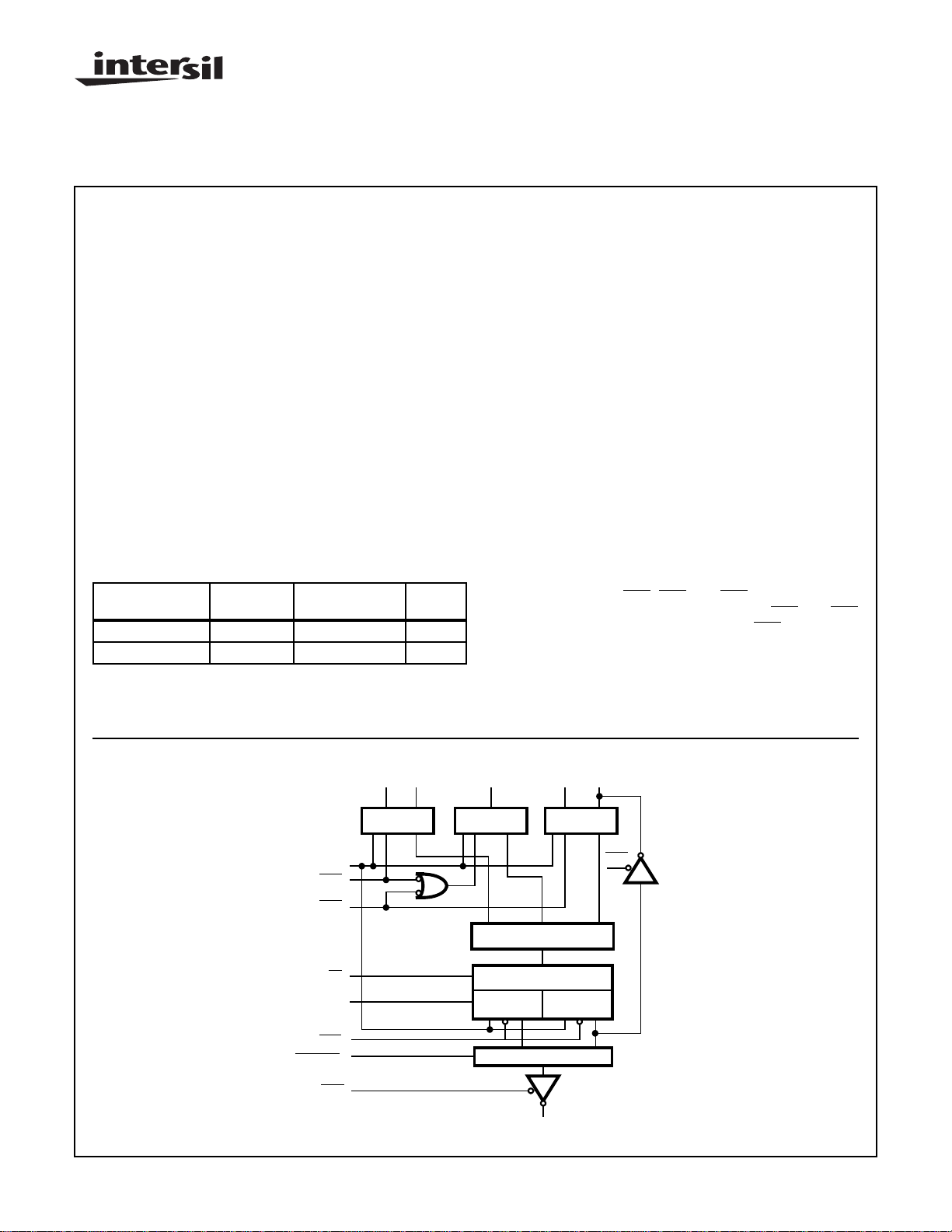
Two 16-bit output registers (MSP and LSP) are provided to hold
the most and least significant portions of the result, respectively.
These registers may be made transparent for asynchronous
operation through the use of the Feedthrough Control (FT). The
two halves of the product may be routed to a single 16-bit threestate output port via the output multiplexer control, and in addition, the LSP is connected to the Y-input port through a separate
three-state buffer.
The HMU17/883 utilizes a single clock signal (CLK) along with
three register enables (
operands and the output product registers. The
inputs enable the X and Y input registers, while
the LSP and MSP output registers. This configuration facilitates
the use of the HMU17/883 for micro-programmed systems.
All outputs of the HMU17/883 also offer three-state control for
multiplexing onto multiuse system busses.
ENX, ENY, and ENP) to latch the input
ENX and ENY
ENP enables both
Functional Block Diagram
X0-15 Y0-15/P0-15
TCX RND TCY
REGISTERREGISTERREGISTER
CLK
ENX
ENY
MULTIPLIER ARRAY
FA
FT
ENP
MSPSEL
OEP
CAUTION: These devices are sensitive to electrostatic discharge; follow proper IC Handling Procedures.
http://www.intersil.com or 407-727-9207
| Copyright © Intersil Corporation 1999
FORMAT ADJUST
MSP
REGISTER
MULTIPLEXER
3-36
REGISTER
P16-31/P0-15
OEL
LSP
File Number 2805.2

HMU17/883
Absolute Maximum Ratings Thermal Information
Supply Voltage . . . . . . . . . . . . . . . . . . . . . . . . . . . . . . . . . . . . . .8.0V
Input or Output Voltage Applied . . . . . . . . .GND 0.5V to VCC +0.5V
ESD Rating. . . . . . . . . . . . . . . . . . . . . . . . . . . . . . . . . . . . . . Class 1
Operating Conditions
Voltage Range . . . . . . . . . . . . . . . . . . . . . . . . . . . . . . . .4.5V to 5.5V
Temperature Range . . . . . . . . . . . . . . . . . . . . . . . . . -55oC to 125oC
CAUTION: Stresses above those listed in “Absolute Maximum Ratings” may cause permanent damage to the device. This is a stress only rating and operation
of the device at these or any other conditions above those indicated in the operational sections of this specification is not implied.
NOTE:
1. θJA is measured with the component mounted on an evaluation PC board in free air.
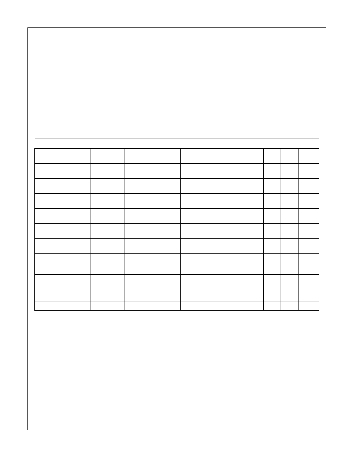
TABLE 1. DC ELECTRICAL PERFORMANCE SPECIFICATIONS
PARAMETER SYMBOL TEST CONDITIONS
Logical One Input
Voltage
Logical Zero Input
Voltage
Output HIGH Voltage V
Output LOW Voltage V
Input Leakage Current I
Output or I/O Leakage
Current
Standby Power Supply
Current
Operating Power Supply
Current
Functional Test FT (Note 4) 7, 8 -55 ≤ TA≤ 125 - -
NOTES:
2. Interchanging of force and sense conditions is permitted.
3. Operating Supply Current is proportional to frequency, typical rating is 5mA/MHz.
4. Tested as follows: f = 1MHz, VIH (Clock Inputs) = 3.0, VIH (All other inputs) = 2.6, VIL = 0.4, VOH≥ 1.5V, and VOL≤ 1.5V.
V
V
OH
OL
I
O
I
CCSB
I
CCOP
IH
IL
I
VCC = 5.5V 1, 2, 3 -55 ≤ TA≤ 125 2.2 - V
VCC = 4.5V 1, 2, 3 -55 ≤ TA≤ 125 - 0.8 V
IOH = 400µA
VCC = 4.5V (Note 2)
IOL = +4.0mA
VCC = 4.5V (Note 2)
VIN = VCC or GND
VCC = 5.5V
V
= VCC or GND
OUT
VCC = 5.5V
VIN = VCC or GND,
VCC = 5.5V, Outputs
Open
f = 1.0 MHz,
VIN = VCC or GND
VCC = 5.5V
(Note 3)
Thermal Resistance (Typical, Note 1) θJA (oC/W) θJC (oC/W)
PGA Package . . . . . . . . . . . . . . . . . . . 42.69 10.0
Maximum Package Power Dissipation at 125
PGA Package . . . . . . . . . . . . . . . . . . . . . . . . . . . . . . . . . . . . .1.17
Maximum Junction Temperature. . . . . . . . . . . . . . . . . . . . . . . . 175oC
Maximum Storage Temperature Range . . . . . . . . . .-65oC to 150oC
Maximum Lead Temperature (Soldering 10s). . . . . . . . . . . . .300oC
Die Characteristics
Number of Gates. . . . . . . . . . . . . . . . . . . . . . . . . . . . . . . . . . . .4,500
GROUP A
SUBGROUPS
1, 2, 3 -55 ≤ TA≤ 125 2.6 - V
1, 2, 3 -55 ≤ TA≤ 125 - 0.4 V
1, 2, 3 -55 ≤ TA≤ 125 -10 +10 µA
1, 2, 3 -55 ≤ TA≤ 125 -10 +10 µA
1, 2, 3 -55 ≤ TA≤ 125 - 500 µA
1, 2, 3 -55 ≤ TA≤ 125 - 7.0 mA
TEMPERATURE
(oC) MIN MAX UNITS
3-37
 Loading...