Intersil Corporation HMU16, HMU17 Datasheet

HMU16, HMU17
Data Sheet November 1999
16 x 16-Bit CMOS Parallel Multipliers
The HMU16 and HMU17 are high speed, low power CMOS
16-bit x 16-bit multipliers ideal forfast,realtimedigitalsignal
processing applications.
The X and Y operands along with their mode controls (TCX
and TCY) have 17-bit input registers. The mode controls
independently specify the operands as either two’s
complement orunsignedmagnitude format, thereby allowing
mixed mode multiplication operations.
Two16-bit output registers are provided to hold the most and
least significant halves of the result (MSP and LSP). For
asynchronous output, these registers may be made
transparent through the use of the Feedthrough Control
(FT).
Additional inputs are provided for format adjustment and
rounding. The Format Adjust control (FA) allows the user to
select either a left shifted 31-bit product or a full 32-bit
product, whereas the round control (RND) provides the
capability of rounding the most significant portion of the
result.
The HMU16 has independent clocks (CLKX, CLKY, CLKL,
CLKM) associated with each of these registers to maximize
throughput and simplify bus interfacing. The HMU17 has
only a single clock input (CLK), but makes use of three
register enables (
inputs control the X and Y Input Registers, while
controls both the MSP and LSP Output Registers. This
configuration facilitates the use of the HMU17 for
microprogrammed systems.
The two halves of the product may be routed to a single
16-bit three-state output port via a multiplexer, and in
addition, the LSP is connected to the Y-input port through a
separate three-state buffer.
ENX, ENY and ENP). The ENX and ENY
ENP
File Number 2803.4
Features
• 16 x 16-Bit Parallel Multiplier with Full 32-Bit Product
• High-Speed (35ns) Clocked Multiply Time
• Low Power Operation
-I
-I
• Supports Two’s Complement, Unsigned Magnitude and
Mixed Mode Multiplication
• HMU16 is Compatible with the AM29516, LMU16,
IDT7216 and the CY7C516
• HMU17 is Compatible with the AM29517, LMU17,
IDT7217 and the CY7C517
• TTL Compatible Inputs/Outputs
• Three-State Outputs
= 500µA Maximum
CCSB
= 7.0mA Maximum at 1MHz
CCOP
Applications
• Fast Fourier Transform Analysis
• Digital Filtering
• Graphic Display Systems
• Image Processing
• Radar and Sonar
• Speech Synthesis and Recognition
Ordering Information
TEMP.
PART NUMBER
HMU16JC-35 0 to 70 68 Ld PLCC N68.95
HMU16JC-45 0 to 70 68 Ld PLCC N68.95
HMU16GC-35 0 to 70 68 Ld CPGA G68.B
HMU16GC-45 0 to 70 68 Ld CPGA G68.B
HMU17JC-35 0 to 70 68 Ld PLCC N68.95
HMU17JC-45 0 to 70 68 Ld PLCC N68.95
HMU17GC-35 0 to 70 68 Ld CPGA G68.B
HMU17GC-45 0 to 70 68 Ld CPGA G68.B
RANGE (oC) PACKAGE
PKG.
NO.
1
CAUTION: These devices are sensitive to electrostatic discharge; follow proper IC Handling Procedures.
1-888-INTERSIL or 407-727-9207
| Copyright © Intersil Corporation 1999

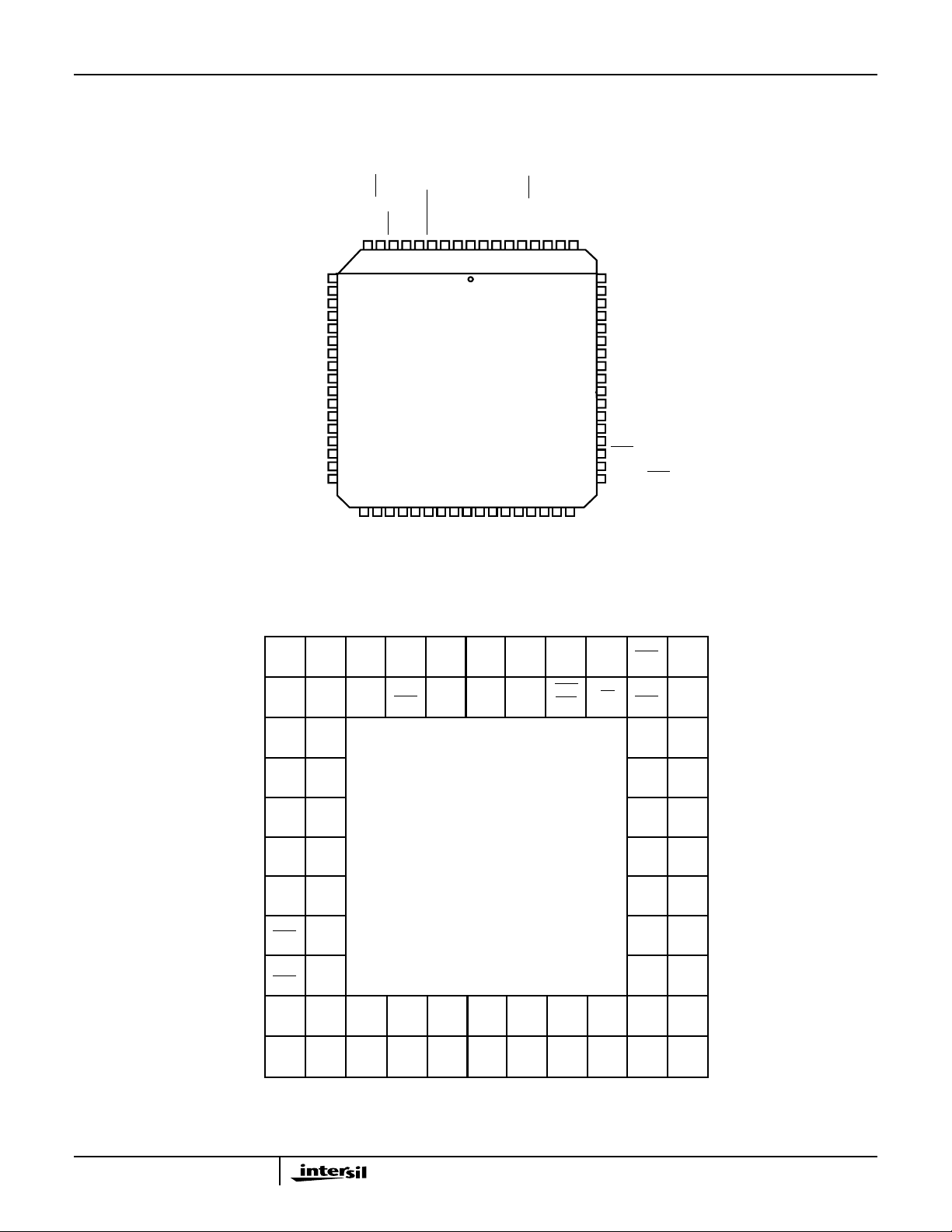
Pinouts
P15, P31
P14, P30
P13, P29
P12, P28
P11, P27
P10, P26
P9, P25
P8, P24
P7, P23
P6, P22
P5, P21
P4, P20
P3, P19
P2, P18
P1, P17
P0, P16
NC
OEP
CLKM (ENP)
NC
10
11
12
13
14
15
16
17
18
19
20
21
22
23
24
25
26
27282930313233
HMU16, HMU17
68 LEAD PLCC
TOP VIEW
FAFTMSPSEL
GND
GND
VCCVCCTCY
TCX
RND
123456789
6867666564636261
ENX)
CLKX (
X15
X14
43424140393837363534
X13
60
59
58
57
56
55
54
53
52
51
50
49
48
47
46
45
44
NC
X12
X11
X10
X9
X8
X7
X6
X5
X4
X3
X2
X1
X0
OEL
CLKL (CLK)
CLKY (
ENY)
11
10
9
8
7
6
5
4
3
N/C
X11
X12
X9
X10
X7
X8
X5
X6
X3
X4
X1
X2
X0
OEL
CLKL
CLKY
(
ENY) (CLK)
Y15, P15
X13
X14
Y14, P14
Y13, P13
Y12, P12
X15
CLKX
(ENX)
Y9, P9
Y8, P8
Y7, P7
Y11, P11
Y10, P10
Y6, P6
68 LEAD CPGA
TOP VIEW
TCY
RND
V
TCX
CC
Y5, P5
Y4, P4
GND
Y3, P3
V
CC
Y2, P2
Y1, P1
GND
MSP
Y0, P0
SEL
NC
FT
FA
OEP
CLKM
ENP)
(
P30/
P14 P15
P28/
P12 P13
P26/
P10 P11
P24/
P8 P9
P22/
P6 P7
P20/
P4
P18/
P2
N/C
P31/
P29/
P27/
P25/
P23/
P21/
P5
P19/
P3
Y10/
Y12/
Y13/
Y14/
Y15/
N/C
Y0/P0
Y2/P2
Y1/P1
Y3/P3
BA KLCD E F GH J
2
1
Y4/P4
Y5/P5
Y6/P6
Y7/P7
Y8/P8
Y9/P9
P10 P12 P14
Y11/
P11 P13 P15
P16/
N/C
P17/
P1P0
2

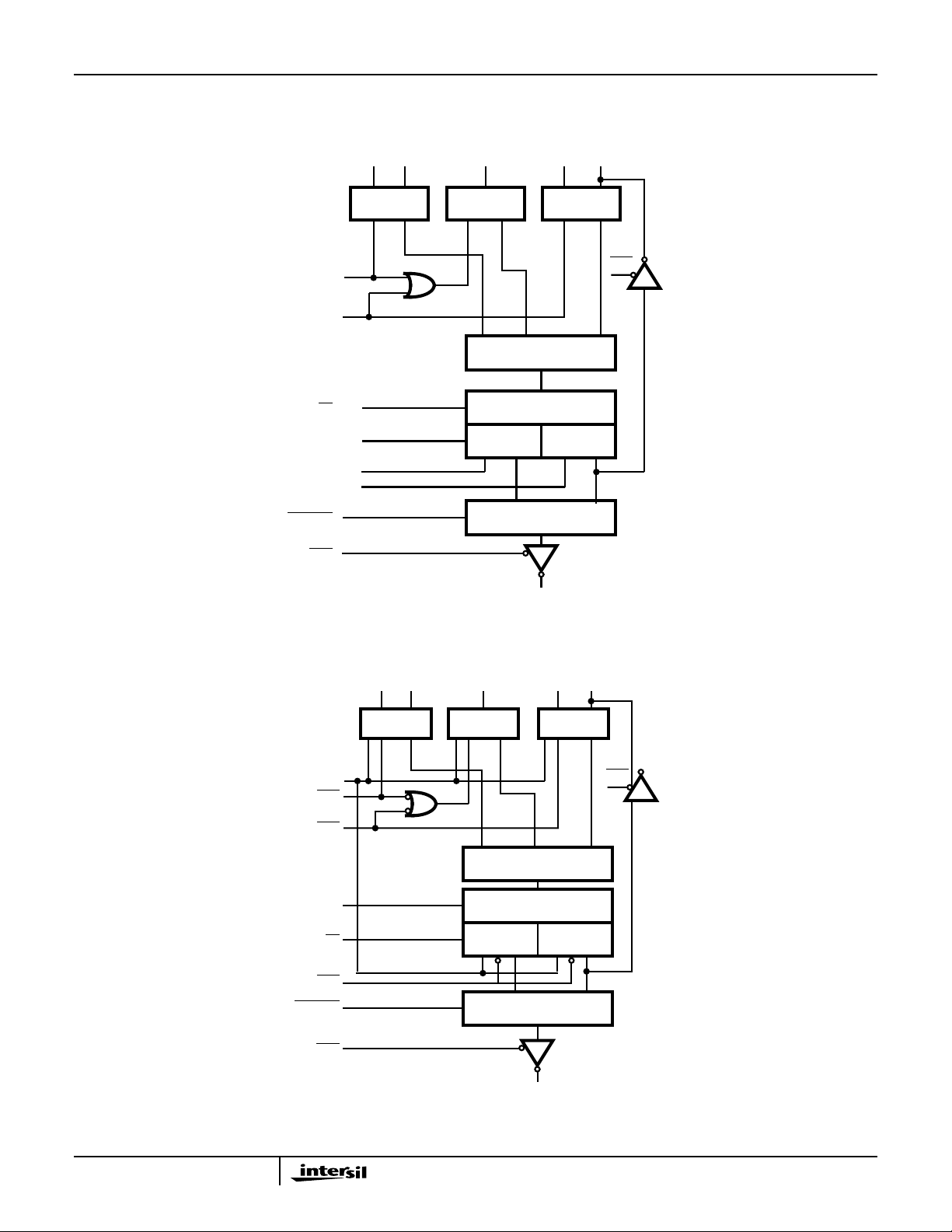
Functional Block Diagrams
HMU16, HMU17
HMU16
CLKX
CLKY
FA
FT
CLKM
CLKL
MSPSEL
OEP
X0 - 15 TCX
REGISTER
RND TCY Y0 - 15/PO - 15
REGISTER REGISTER
OEL
MULTIPLIER ARRAY
FORMAT ADJUST
MSP
RESISTER
MULTIPLEXER
P16 - 31/PO - 15
LSP
RESISTER
CLK
ENX
ENY
FA
FT
ENP
MSPSEL
OEP
HMU17
X0 - 15
TCX TCX RND TCY Y0 - 15/PO - 15
REGISTERREGISTER
MULTIPLIER ARRAY
FORMAT ADJUST
MSP
RESISTER
REGISTER
RESISTER
MULTIPLEXER
OEL
LSP
P16 - 31/PO - 15
3

HMU16, HMU17
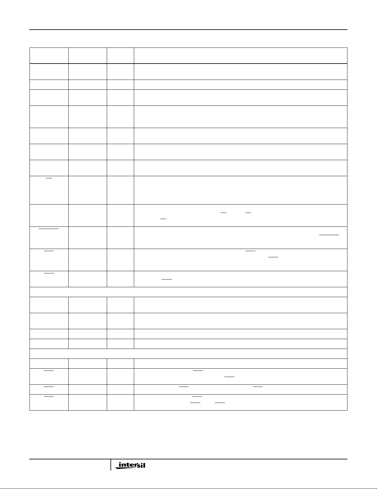
Pin Description
PLCC PIN
SYMBOL
V
CC
GND 2, 3 GND. The device ground.
X0-X15 47-59, 61-63 I X-Input Data. These 16 data inputs provide the multiplicand which may be in two's complement
Y0-Y15/
P0-P15
P16-P31/
P0-P15
TCY, TCX 66, 67 I Two's Complement Control. Input data is interpreted as two's complement when this control is
FT 5 I Feed through Control. When this control is HIGH, both the MSP and LSP Registers are
FA 6 I FormatAdjust Control. A full 32-bit product is selected when this control line is HIGH. A LOW on
RND 65 I Round Control. When this control is HIGH, a one is added to the Most Significant Bit (MSB) of the
MSPSEL 4 I Output Multiplexer Control. When this control is LOW, the MSP is available for output at the
OEL 46 I Y-In/P0-15Output Port Three-State Control. When OELis HIGH, the output drivers are inthe high
OEP 7 I P16-31/P0-15 Output Port Three-State Control. A LOW on this control line enables the output
THE FOLLOWING PIN DESCRIPTIONS APPLY TO THE HMU16 ONLY
CLKX 64 I X-Register Clock. The rising edge of this clock loads the X-data Input Register along with the TCX
CLKY 44 I Y-Register Clock. The rising edge of this clock loads the Y-data Input Register along with the TCY
CLKM 8 I MSPRegister Clock. The rising edge of CLKM loads the Most Significant Product (MSP) Register.
CLKL 45 I LSP Register Clock. The rising edge of CLKL loads the Least Significant Product (LSP) Register.
THE FOLLOWING PIN DESCRIPTIONS APPLY TO THE HMU17 ONLY
CLK 45 I Clock. The rising edge of this clock will load all enabled registers.
ENX 64 I X-Register Enable. When ENX is LOW, the X-register is enabled; X-input data and TCX will be
ENY 44 I Y-Register Enable. ENY enables the Y-register. (See ENX).
ENP 8 I Product Register Enable. ENP enables the Product Register. Both the MSP and LSP
NUMBER TYPE DESCRIPTION
1, 68 VCC. The +5V power supply pins. A 0.1µF capacitor between the VCC and GND pins is
recommended.
or unsigned magnitude format.
27-42 I/O Y-Input/LSP Output Data. This 16-bit port is used to provide the multiplier which may be in two's
complement or unsigned magnitude format. It may also be used for output of the Least Significant
Product (LSP).
10-25 O Output Data. This 16-bit port may provide either the MSP (P16-31) or the LSP (P0-15).
HIGH. A LOW indicates the data is to be interpreted as unsigned magnitude format.
transparent. When LOW, the registers are latched by their associated clock signals.
this control line selects a left shifted 31-bit product with the sign bit replicated in the LSP. This
control is normally HIGH, except for certain two's complement integer and fractional
applications.
LSP. This position is dependent on the FAcontrol; FA = HIGH indicates RND adds to the 2-15 bit
(P15), and FA = LOW indicates RND adds to the 2
dedicated output port, and the LSP is available at the Y-input/LSP output port. When MSPSEL is
HIGH, the LSP is available at both ports and the MSP is not available for output.
impedance state. This state is required for Ydata input. When OEL is LOW, the port is enabled for
LSP output.
port. When OEP is HIGH, the output drivers are in the high impedance state.
and RND Registers.
and RND Registers.
latched at the rising edge of CLK. When ENX is high, the X-register is in a hold mode.
Sections are enabled by ENP. (See ENX).
-16
bit (P14).
4
 Loading...