Intersil Corporation HMP9701A Datasheet
Semiconductor
HMP9701A
OBSOLETE PRODUCT
November 1998
call Central Applications 1-800-442-7747
or email: centapp@harris.com
Features
FOR A POSSIBLE SUBSTITUTE PRODUCT
• Compliant with the Audio Codec ‘97 Standard
• High Fidelity 16-Bit Σ∆ Converters
[ /Title (HMP9701A)
- DAC SNR 87dB
/Subject (AC’97 Audio Codec)
- ADC SNR 85dB
/Author ()
• Additional A/D for Microphone Pass-Through
/Keywords (Harris Semiconductor, Audio Codecs, PC
• AC Link Serial Interface Compatible with A C’97 Digital
Audio, PC’98, PC98, PC 98, PC’99, PC 99, PC99,
Controllers
THD, PCI Audio, AC97, A C’97, AC 97, AC’98, A C 98,
• Fixed 48kHz Sampling Rate
AC98, SNR, AC Link, PC’97, PC 97, PC97, GAM
• 6 Channel Input Mixer
PCI Sound, Total Harmonic Distortion, Signal to Noise
• Programmable Powerdown Modes
Ratio, Record Gain
)
• 48 Lead TQFP Package
/Creator ()
• Single +5V Supply
/DOCINFO pdfmark
Applications
[ /PageMode /UseOutlines
• Multimedia PC Applications
/DOCVIEW pdfmark
- Desk Top PCs
- Notebook PCs
- PCI Sound Cards
- Motherboards
• Video Conferencing
• Speaker Phones
Table of Contents
Functional Block Diagram . . . . . . . . . . . . . . . . . . . . . . . . . . 2
Functional Description. . . . . . . . . . . . . . . . . . . . . . . . . . . . . 2
Serial Digital Interface . . . . . . . . . . . . . . . . . . . . . . . . . . . . .3
Page
AC’97 Audio Codec
Description
The HMP9701A is the next generation PC based audio codec
solution. The HMP9701A is compliant to the new AC’97 standard and, as such, interfaces to any AC’97 compliant digital
controller. The HMP9701A off ers the designer a solution to satisfy the demand for flexibility and improved High Fidelity sound
in a PC environment. As part of the AC’97 PC audio standard
architecture, the HMP9701A helps pave the way for PC’97
compliant desktop, portable and entertainment PCs with a cost
effective high-quality audio solution.
As the analog front end of the AC’97 chipset, the HMP9701A
accepts line level audio inputs from se v en diff erent sources and
converts the analog audio to 16-bit digital streams of either stereo or mono data. The 48 kss data is transmitted to the controller via the AC’97 standard five wire interface. The controller
sends digital audio data to the HMP9701A to be converted to
analog stereo or monaural line output using two DA Cs .
We include an additional ADC to be used for Acoustic Echo
Canceling needed for video conferencing applications. This
ADC has a dedicated microphone input. It has the same high
quality performance as the stereo ADCs. The small 48 lead
TQFP (Thin 1.5mm and 7mm x 7mm footprint Quad Flat Package) makes it easy to locate the analog codec close to the analog sources. Thus, reducing noise and lowering the cost of
implementation.
Ordering Information
TEMP.
PART NUMBER
HMP9701ACN 0 to 70 48 Ld TQFP† Q48.7x7A
HMP9701EVAL2 PCI Bus Evaluation Board (Includes codec)
† TQFP is also known as PQFP and MQFP.
RANGE (oC) PACKAGE PKG. NO.
Control Register Description . . . . . . . . . . . . . . . . . . . . . . . . 8
Pinout . . . . . . . . . . . . . . . . . . . . . . . . . . . . . . . . . . . . . . . .11
Pin Descriptions . . . . . . . . . . . . . . . . . . . . . . . . . . . . . . . . 11
AC and DC Electrical Specifications . . . . . . . . . . . . . . . . . 13
ADC/DAC Filter Response Curves . . . . . . . . . . . . . . . . . . 17
AC Timing Waveforms. . . . . . . . . . . . . . . . . . . . . . . . . . . . 18
Schematic Diagram. . . . . . . . . . . . . . . . . . . . . . . . . . . . . . 19
Package Dimensions. . . . . . . . . . . . . . . . . . . . . . . . . . . . . 21
CAUTION: These devices are sensitive to electrostatic discharge. Users should follow proper IC Handling Procedures.
Copyright
© Harris Corporation 1998
1
File Number 4473.1
Functional Block Diagram
HMP9701A AC’97 AUDIO CODEC
HMP9701A
MIC1
MIC2
LINE_IN
CD
VIDEO
AUX
PHONE
MONO_OUT
LINE_OUT
PC_BEEP
MIC
SEL
MONO
VOL
MASTER
VOL
GAM
GAIN
0dB/20dB
SEL
MONO
G
A
M
∑
STEREO SIGNAL PATH
MONO SIGNAL PATH
G
G
G
A
M
G
A
A
A
M
M
M
∑
∑
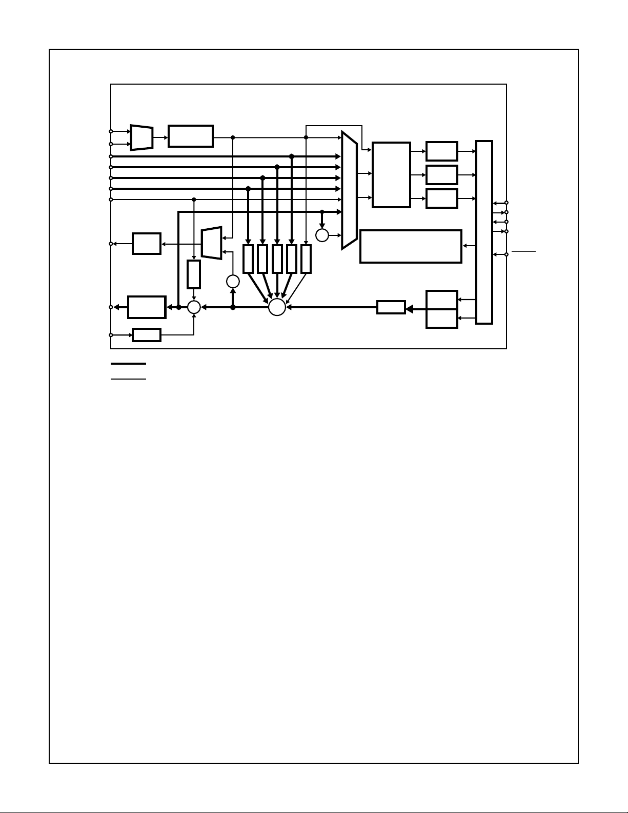
Functional Description
The HMP9701A is a full-duplex stereo audio codec compliant
to the AC’97 Codec specification. This component is designed
for use in multimedia and business personal computers. The
codec includes full duplex stereo converters, a mic pass
through ADC, complete on-chip anti-alias filtering, and a 5
channel analog mixer with programmable gain and atten uation.
Analog Inputs
The HMP9701A has 4 stereo inputs (LINE_IN, CD, VIDEO,
and AUX), two microphone le vel inputs (MIC1 and MIC2), and
one mono line level input (PHONE). A multiplexer is provided
to independently select the right and left record sources from
the analog inputs listed above. In addition, the output stereo
mix (LINE_OUT) or its mono equivalent may also be selected
as a record source. A gain block is available to amplify the
MIC inputs by 20dB to compensate for the diff erence between
line levels and typical condenser microphone levels.
Besides being fed to the Record Select Mux, all analog
inputs can be mixed (see Analog Mixer) with the stereo output from the Playback DACs. Note: all analog inputs except
PHONE and PC_BEEP can be output on MONO_OUT.
There is a dedicated analog input, PC_BEEP, for the
standard “Beep” signal provided on most PC/Compatible
computers for power on self test and boot audio status
indication. This input is mixed into each channel of the
stereo line outputs.
Σ∆ A/D
RECORD
GAIN
RECORD SELECT
∑
G
A
M
CONTROL/CONFIGURA TION
(64 REGISTERS)
GAM
AC’97
Σ∆ A/D
Σ∆ A/D
Σ∆ D/A
Σ∆ D/A
SYNC
BIT_CLK
SDATA_OUT
SDATA_IN
RESET
AC LINK INTERFACE
Record ADCs
The HMP9701A provides 3 Σ∆ ADCs to record one dedicated microphone input and 2 user selectable analog inputs.
The user selectable analog inputs are routed to the stereo
ADCs via an programmable Input Multiplexer. The multiplexer is programmed to select the 2 record channels via the
Record Select register (1Ah).
Each of the record channels pass through a programmable
gain block before each ADC. The record gain for each channel is set individually and ranges from 0dB to 22.5dB in
1.5dB increments (see Record Gain Registers 1Ch and
1Eh). The gain block can also be used to mute each channel. Note: an additional gain block provides 20dB of gain on
the MIC channel if activated (see MIC Volume register 0Eh).
The HMP9701A uses oversampling Σ∆ ADCs which only
require a single pole passive filter for anti-alias filtering. The
filter for the left, right and MIC channels is realized by placing
a 1nF capacitor between the AFILT1, AFILT2, and AFILT3
pins and analog ground respectively.
Playback DACs
The HMP9701A uses oversampling single bit Σ∆ DACs to
convert the stereo playback sample to an analog line level
output. The output of the DACs pass through internal reconstruction filters that do not require any external components.
2
HMP9701A
Analog Mixer
The Analog Mixer generates two outputs, one stereo and
one mono. The stereo output is used to drive LINE_OUT and
is composed of a stereo mix of all analog input sources and
the audio output from the DACs. The mono output drives
MONO_OUT, and it is user selectable as either MIC only or
a mono mix of all the analog and PCM sources except the
PHONE and PC_BEEP inputs.
The inputs to the analog mixer pass through gain/attenuate/mute (GAM) blocks. Each gain block provides volume
control from -34.5dB to +12dB in 1.5dB increments (see
Input Volume Registers 0Ch - 18h). Additionally, the GAM
blocks can be used to mute individual mixer inputs. An additional gain of 20dB is provided for the selected MIC input.
Note: for best SNR performance, the GAM block for the DAC
output should be used to control PCM analog volume rather
than digitally attenuating the DAC PCM input to take advantage of full resolution conversions.
Clocking
The HMP9701A derives it’s internal clock from an externally
attached 24.576MHz crystal. The crystal and 2 capacitors
are attached to the XTL_IN and XTL_OUT pins, and it
should be fundamental-mode /parallel resonant with a load
capacitor as specified by the crystal manufacturer (typically
12-30pF). For an example circuit, refer to the Typical Application Schematic.
An external CMOS clock may be connected to XTL_IN
instead of a crystal. If this external clocking option is used,
XTL_OUT should be left floating. Please Note: No capacitors are used on the crystal pins in this mode.
The HMP9701A divides the clock source by 2 to derive the
BIT_CLK provided to the companion digital controller. The
digital controller should divide the provided BIT_CLK by 256
to generate the 48kHz SYNC signal used to define the audio
frame transmitted over the serial digital interface (See Serial
Digital Interface Section)
Serial Digital Interface
Audio Data Format
The HMP9701A supports 16-bit 2’s complement linear PCM
data for record and playback. The 16-bit 2’s complement format (also called 16-bit signed format) is the standard method
of representing 16-bit digital audio. This format gives 96dB
theoretical dynamic range and is the standard for compact
disk audio players. This format uses the value -32768
(8000h) to represent minimum analog amplitude while
32767 (7FFFh) represents maximum analog amplitude.
SYNC
BIT_CLK
AC’97
DIGITAL
CONTROLLER
FIGURE 1. HMP9701A CONNECTION TO AC’97 CONTROLLER
SDATA_OUT
SDATA_IN
RESET
Digital Serial Interface (AC Link)
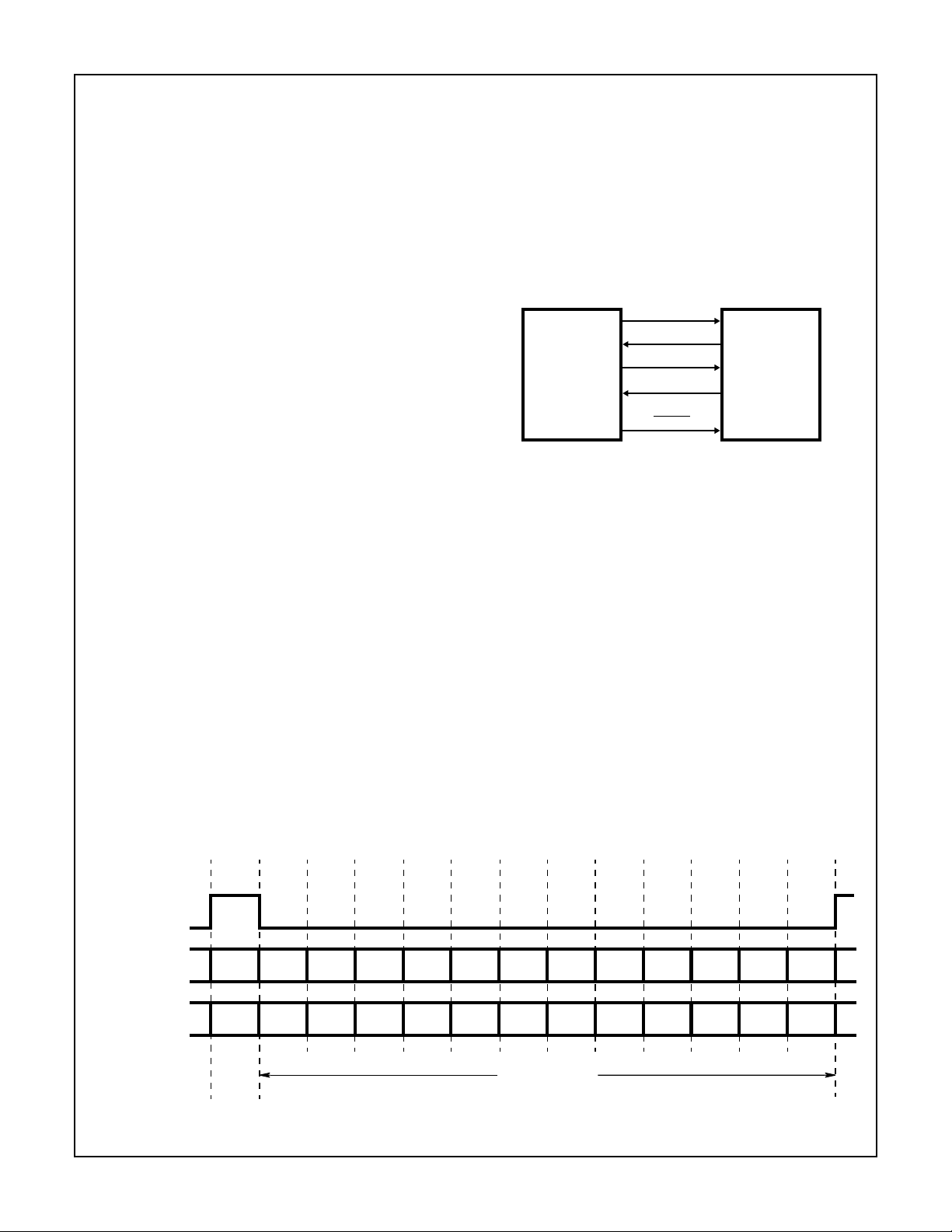
The HMP9701A is linked to an AC’97 digital controller via a 5
pin digital serial interface as shown in Figure 1. This interface, the AC-link, supports bidirectional, fixed rate, serial
data streams. The data transfers are based on a time division multiplexed (TDM) protocol that provides for multiple
input and output audio streams together with control and status data. The AC-link protocol is based on incoming and outgoing audio frames which are each divided into 12 data slots
as shown in Figure 2. The HMP9701A allocates data slots
for 2 PCM playback channels, 2 PCM record channels,
codec control, codec status, and a PCM microphone record
channel. The remaining unused time slots are reserved.
HMP9701A
AC’97
AUDIO
CODEC
SLOT NO.
SYNC
OUTGOING
AUDIO STREAMS
INCOMING
AUDIO STREAMS
0123456789101112
TAG
TAG
TAG
PHASE
CMD
ADDR
STATUS
ADDR
CMD
DAT A
STATUS
DAT A
PCM
PCM
PCM
RIGHT
PCM
RIGHT
DATA PHASE
LEFT
LEFT
FIGURE 2. AC LINK BIDIRECTIONAL DATA FRAME
RSRVDRSRVDRSRVDRSRVDRSRVDRSRVDRSRVDRSRVD
RSRVDRSRVDRSRVDRSRVDRSRVDRSRVDMICRSRVD
3
HMP9701A
20.8µs
(48kHz)
TAG PHASE DATA PHASE
SYNC
BIT_CLK
SDATA_OUT
VALID
FRAME
“1” = FRAME CONTAINS
VALID DATA
12.288MHz
81.4ns
SLOT
SLOT SLOT
21
TIME SLOT “VALID” BITS
(“1” = TIME SLOT CONTAINS VALID DATA)
12
FIGURE 3. AC LINK AUDIO OUTPUT FRAME
“0” “0” “0” BIT 19 BIT 0 BIT 19 BIT 0 BIT 19 BIT 0
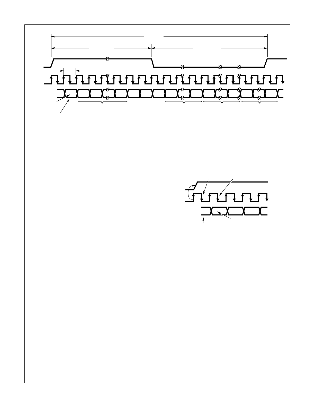
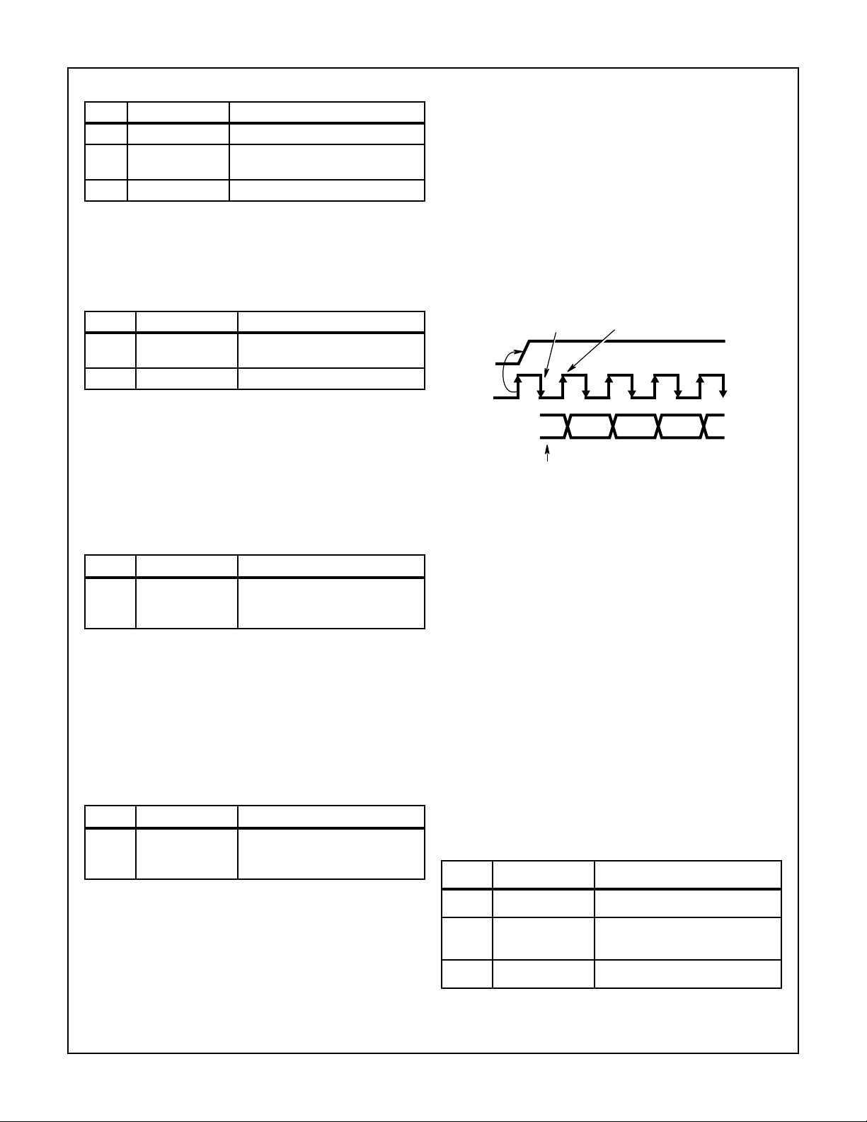
The HMP9701A generates a serial bit clock (BIT_CLK) at
12.288MHz for synchronous data transfers on the AC Link.
Data is output on SDATA_IN by the rising edge of BIT_CLK,
and serial data is sampled on SDATA_OUT by the falling
edge of BIT_CLK. An audio frame transfer is initiated by the
assertion of SYNC for the 16 BIT_CLK’s comprising the Tag
Phase of the audio frame. The SYNC signal must be
asserted at a fixed 48kHz rate, and it can be derived by
dividing down the BIT_CLK.
The tag phase is a 16-bit data slot (Slot 0) wherein each bit
is a data valid flag for an associated time slot within the current audio frame. A “1” in a given bit position of Slot 0 indicates that the corresponding time slot within the audio frame
contains valid data. If the HMP9701A “tags” a slot invalid, it
will set the data bits comprising that slot to zero.
SLOT 1 SLOT 2 SLOT 12
in the control and PCM output data slots is valid. The
remaining 8 bits in Slot 0 are ignored as they are associated with reserved data slots.
SYNC
BIT_CLK
SDATA_OUT
HMP9701A SAMPLES
SYNC ASSERTION
PREVIOUS
AUDIO FRAME
HMP9701A SAMPLES
FIRST BIT OF AUDIO OUTPUT
SLOT 1 SLOT 2
VALID
FRAME
AC Link Output Frame (SDATA_OUT)
The audio output frame contains data targeted for the
HMP9701A’s DAC inputs, and control registers. This data is
transmitted in slots 1 through 4 of the audio frame as shown
in Figure 2. The tag slot, Slot 0, is a special reserved time
slot containing 16 bits that tell the AC-link interface circuitry
the validity of the following data slots.
The HMP9701A is synchronized to the beginning of a new
audio output frame when SYNC makes a low to high transition and is sampled low by the falling edge of BIT_CLK as
shown in Figure 3. On the next rising of BIT_CLK, the
AC’97 controller drives SDATA_OUT with the first bit of slot
0 (Valid Frame bit) which is then sampled by the
HMP9701A on the subsequent falling edge of BCLK. The
controller drives the remaining audio frame bits out on
SDATA_OUT with each rising edge of BCLK, and the
HMP9701A samples these bits on the subsequent falling
edge.
The first bit of the output audio frame (Slot 0, bit 15) flags
the validity of the entire audio frame. If the “Valid Frame” bit
is a 1, this indicates that the current audio frame contains
at least one time slot of valid data. The HMP9701A monitors the next 4-bit positions to determine whether the data
FIGURE 4. START OF AUDIO OUTPUT FRAME
The 20-bit data word in each time slot must be transmitted MSB
first. If the data word targeted for a time slot is less than 20 bits,
the data word must be MSB justified in the most significant bits
of the time slot with the unused bits set to zero. F or e xample, an
8-bit audio sample would be transmitted in bits 19-12 of the
time slot with the trailing 12 bits set to zero. The MSB of the
audio sample would map to bit 19 of the time slot. Note: for the
playback of mono audio streams, the digital controller must
send the same sample to each PCM output channel.
Audio Output Slot 1: Control Address
The bits in Slot 1 are used to access the 16-bit control/status
registers within the HMP9701A. The address space allocated in slot 1 allows up to 64 sixteen bit registers, however,
only the even registers are valid (see Control/Status register
section for a complete register map). The control registers
are read/writable to provide more robust testability. A read or
write command is initiated by setting the Read/Write bit (Bit
19) in Slot 1. A complete bit map for Slot 1 is given in the
Table 1. Note: control data will only be loaded into the target
registers if Slot 2 (Control Data) is flagged as being valid.
4
HMP9701A
TABLE 1. BIT MAP FOR SLOT 1: CONTROL ADDRESS
BITS DESCRIPTION COMMENT
19 Read/Write 1 = Read, 0 = Write
18:12 Control Register
Index
11:0 Reserved Set to “0”
Identifies the Target Control Register
Audio Output Slot 2: Control Data
This Slot is used to deliver the 16-bit control data if the current control register access is a write operation (Bit 19 of Slot
1 is set to “0”). The bit map for Slot 2 is given in Table 2.
TABLE 2. BIT MAP FOR SLOT 2: CONTROL DATA
BITS DESCRIPTION COMMENT
19:4 Control Register
Write Data
3:0 Reserved Set to “0”
Set to “0” if Read operation
Audio Output Slot 3: PCM Playback Left Channel
This time slot contains the audio sample that will be input to
the left channel DAC. The HMP9701A DAC resolution is 17
bits. All audio samples of 17 or less bits should be MSB justified within the 20-bit frame, and the trailing bits should be
set to “0”. Audio samples greater than 17 bits will be rounded
to 17 bits.
TABLE 3. BIT MAP FOR SLOT 3: PCM PLAYBACK LEFT
CHANNEL
BITS DESCRIPTION COMMENT
19:0 PCM Audio
Sample for Left
Channel
Set unused bit positions to “0”
Audio Output Slot 4: PCM Playback Right Channel
This time slot contains the audio sample that will be input to
the right channel DAC. The DAC’s resolution is 17 bits. All
audio samples of 17 or less bits should be MSB justified
within the 20-bit frame, and the trailing bits should be set to
“0”. Audio samples greater than 17 bits will be rounded to 17
bits.
TABLE 4. BIT MAP FOR SLOT 4: PCM PLAYBACK RIGHT
CHANNEL
BITS DESCRIPTION COMMENT
19:0 PCM Audio
Sample for Right
Channel
Set unused bit positions to “0”
samples are returned in slots 3, 4 and 6 as shown in
Figure 2. As before, the tag slot, Slot 0, is a special reserved
time slot containing 16 bits that tell the AC-link interface circuitry the validity of the following data slots.
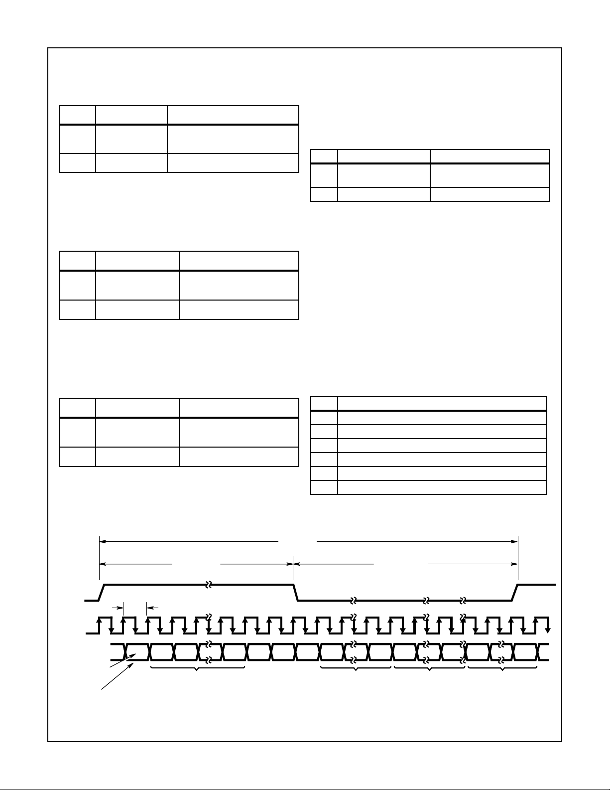
The HMP9701A starts a new audio input frame when SYNC
makes a low to high transition and is sampled low by the falling
edge of BIT_CLK as shown in Figures 5 and 6. On the next rising edge of BIT_CLK, the HMP9701A drives SDATA_IN with
the first bit of slot 0 (Codec Ready bit). The HMP9701A drives
the remaining audio frame bits out on SDATA_IN with each rising edge of BIT_CLK. Note: SYNC must be synchronous to
BIT_CLK.
HMP9701A SAMPLES
SYNC ASSERTION
SYNC
BIT_CLK
SDATA_IN
PREVIOUS AUDIO FRAME
FIGURE 5. START OF AUDIO INPUT FRAME
CODEC
READY
HMP9701A OUTPUTS
FIRST BIT OF AUDIO INPUT FRAME
SLOT 1 SLOT 2
The first bit of an input audio frame (Slot 0, bit 15) indicates
whether the HMP970’s AC Link is functional. If the “Codec
Ready” bit is a 0, the HMP9701A is not ready for normal
operation. If the “Codec Ready” bit is “1”, the HMP9701A is
ready to perform control and status register transfers. At this
point, it is the responsibility of the digital controller to examine the Pow erdown Control/Status register (see Control Register Section) to determine the operational state of the codec
subsections. The 12 bits following the “Codec Ready” Bit in
Slot 0 identify which of the 12 time slots contain valid data.
The HMP9701A outputs each time slots data word MSB first
on SDATA_IN. All non-valid bit positions (for active or inactive time slots) are stuffed with 0’s by the HMP9701A.
Input Audio Slot 1: Status Address
This slot echoes the index of the control register whose contents are returned in slot 2. The data in this register is the
result of a control register read operation initiated by an Output Audio Frame transfer.
TABLE 5. BIT MAP FOR SLOT 1: STATUS ADDRESS
BITS DESCRIPTION COMMENT
Audio Output Slots 5-12: Reserved
Audio output slots 5-12 are reserved for future use and
should be set to “0” for proper operation.
AC Link Input Frame (SDATA_IN)
The audio input frame contains captured audio samples and
codec status for output onto the AC-Link. The codec status
is transmitted in slots 1 and 2, and the 16-bit captured audio
19 Reserved Stuffed with 0
18:12 Control Register
Index
11:0 Reserved Stuffed with 0’s
Echo of Control Register Index for
which data is being returned
5
HMP9701A
Input Audio Slot 2: Status Data
This slot delivers control register read data.
TABLE 6. BIT MAP FOR SLOT 1: STATUS DATA
BITS DESCRIPTION COMMENT
19:4 Control Register
Read Data
3:0 Reserved Stuffed with 0’s
Stuffed with 0’s if slot tagged invalid
Input Audio Slot 3: PCM Record Left Channel
This slot contains an audio sample captured by the left channel ADC. The resolution of the ADC is 16 bits and is MSB
justified in the 20-bit slot.
T ABLE 7. BIT MAP FOR SLOT 3: LEFT CHANNEL RECORD DATA
BITS DESCRIPTION COMMENT
19:4 PCM Record Sample
Left Channel
3:0 Reserved Stuffed with 0’s
16-Bit audio sample from Left
Record ADC
Input Audio Slot 4: PCM Record Right Channel
This slot contains an audio sample captured by the right
channel ADC. The resolution of the ADC is 16 bits and is
MSB justified in the 20-bit slot.
T ABLE 8. BIT MAP FOR SLOT 4: RIGHT CHANNEL RECORD DATA
BITS DESCRIPTION COMMENT
19:4 PCM Record Sample
Right Channel
3:0 Reserved Stuffed with 0’s
16-Bit audio sample from Right
Record ADC
Input Audio Slot 6: Microphone Record Channel
This slot contains an audio sample captured by the dedicated microphone ADC. The resolution of the ADC is 16 bits
and is MSB justified in the 20-bit slot. This input allows
higher performance echo cancellation algorithms in speaker
phone applications.
TABLE 9. BIT MAP FOR SLOT 6: MICROPHONE RECORD DATA
BITS DESCRIPTION COMMENT
19:4 PCM Record Sample
Microphone Channel
3:0 Reserved Stuffed with 0’s
16-Bit Audio Sample From
Dedicated Microphone ADC
Slots 5, 7-12: Reserved
Audio input slots 5, and 7-12 are reserved, and they are set
to “0”.
Low Power Modes
The HMP9701A may be put in a programmable powerdown
state to reduce power when no activity is required. The state of
powerdown is controlled by the Powerdown Register (26h).
This register provides 6 commands to powerdown various sections of the HMP9701A. A summary of the power down commands is given in Table 10 with a more complete description
given in the Control Register Section. Note, the HMP9701A is a
fully static design which will preserve the contents of the internal control registers if the internal clock is stopped.
TABLE 10. SUMMARY OF POWERDOWN REGISTER (26H)
BIT FUNCTION
PR0 Input Mux and ADC Powerdown
PR1 DAC Powerdown
PR2 Analog Mixer Powerdown (V
PR3 Analog Mixer Powerdown (V
PR4 Digital Interface (AC-Link) Powerdown (External CLK Off)
PR5 Internal CLK Disable
REF
REF
On)
Off)
SYNC
BIT_CLK
SDATA_IN
CODEC
READY
“1” = AC LINK INTERFACE
IS FUNCTIONAL
12.288MHz
(“1” = TIME SLOT CONTAINS VALID DATA)
20.8µs
(48kHz)
TAG PHASE DATA PHASE
81.4ns
SLOT
SLOT SLOT
21
TIME SLOT “VALID” BITS
“0” “0” “0” BIT 19 BIT 0 BIT 19 BIT 0 BIT 19 BIT 0
12
SLOT 1 SLOT 2 SLOT 12
FIGURE 6. AC LINK AUDIO INPUT FRAME
6
 Loading...