Intersil Corporation HMP8170, HMP8171, HMP8172, HMP8173 Datasheet
HMP8170, HMP8171, HMP8172, HMP8173
Data Sheet May 1999
NTSC/PAL Video Encoder
The HMP8170, HMP8171, HMP8172, and HMP8173 NTSC
and PALencoders are designed for use in systems requiring
the generation of high-quality NTSC and PAL video.
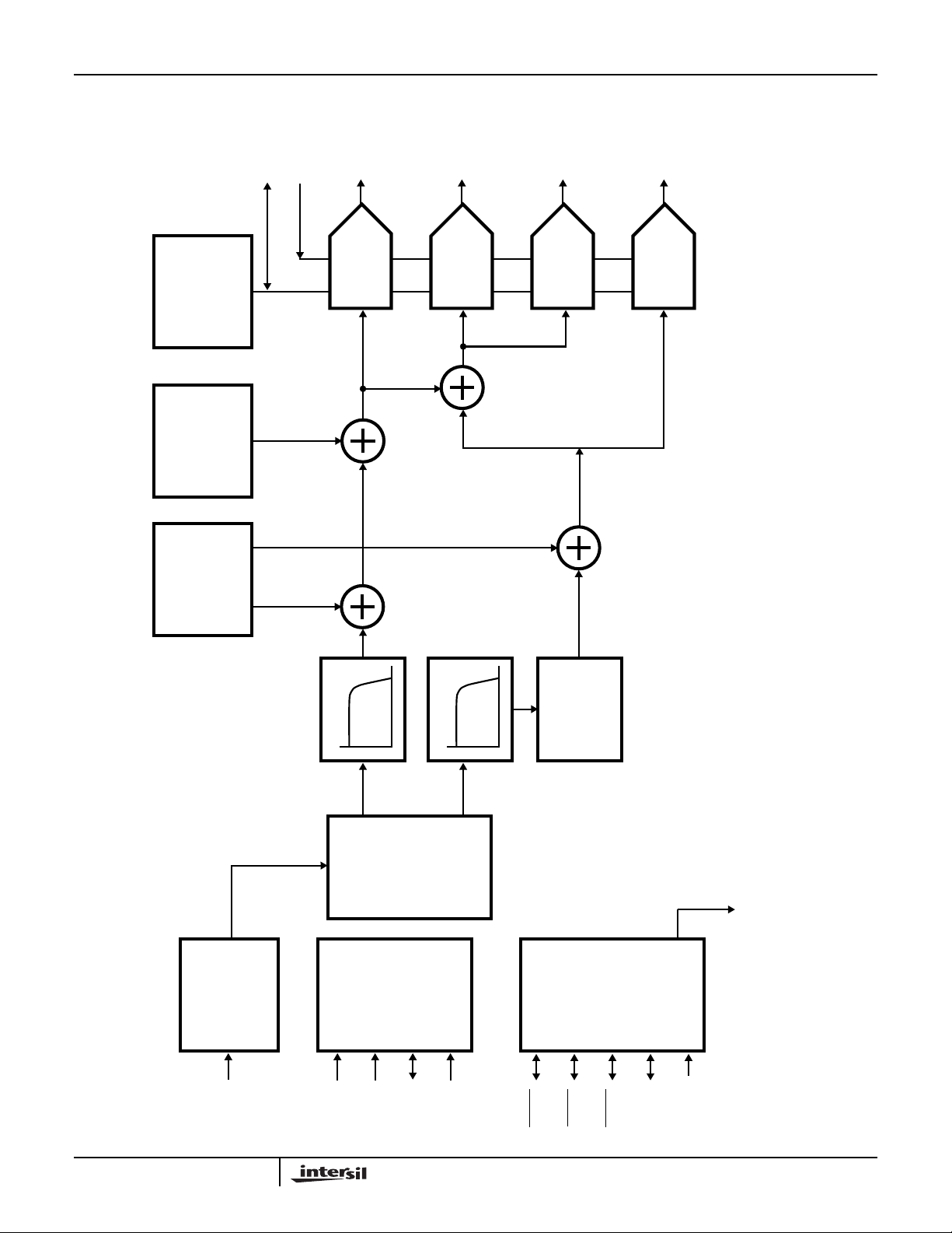
YCbCr digital video data drive the P0-P15 inputs. The Y data
is optionally lowpass filtered to 6MHz and drives the Y analog
output. Cb and Cr are each lowpass filtered to 1.3MHz,
quadrature modulated, and added together. The result drives
the C analog output. The digital Y and C data are also added
together and drive the two composite analog outputs.
The DACs can drive doubly-terminated (37.5Ω) lines, and
run at a 2x oversampling rate to simplify the analog output
filter requirements.
Applications
• DVD Players
• Video CD Players
• Digital VCRs
• Multimedia PCs
Related Products
• NTSC/PAL Encoders
- HMP8154, HMP8156A
• NTSC/PAL Decoders
- HMP8115
File Number 4284.5
Features
• (M) NTSC and (B, D, G, H, I, M, N, NC) PAL Operation
• BT.601 and Square Pixel Operation
• Digital Input Formats
- 8-bit, 16-bit 4:2:2 YCbCr
- 8-bit BT.656
• Analog Output Formats
- Y/C + Two Composite
- RGB + Composite
- YUV + Composite
• Flexible Video Timing Control
- Timing Master or Slave
- Selectable Polarity on Each Control Signal
- Programmable Blank Output Timing
• “Sliced” VBI Data Support
- Closed Captioning
- Widescreen Signalling (WSS)
- BT.653 System B and C Teletext
- NABTS (North American Broadcast Teletext)
- WST (World System Teletext)
• Four 2x Oversampling, 10-Bit DACs
2
• Fast I
C Interface
Ordering Information
MACROVISION
PART NUMBER
HMP8170CN no no 0 to 70 64 Ld PQFP (Note 2) Q64.14x14
HMP8171CN (Note 1) yes no 0 to 70 64 Ld PQFP (Note 2) Q64.14x14
HMP8172CN no yes 0 to 70 64 Ld PQFP (Note 2) Q64.14x14
HMP8173CN (Note 1) yes yes 0 to 70 64 Ld PQFP (Note 2) Q64.14x14
HMP817xEVAL1 Daughter Card Evaluation Platform, where x is replaced by 0, 1, 2, or 3 (Note 3).
NOTES:
1. The HMP8171 and HMP8173 may be purchased by Macrovision Authorized Buyers only. These devices are protected by U.S. patent numbers
4,631,603, 4,577,216, and 4,819,098, and other intellectual property rights. The use of Macrovision’s copy protection technology in the devices
must be authorized by Macrovision and is intended for home and other limited pay-per-view uses only, unless otherwise authorized in writing
by Macrovision. Reverse engineering or disassembly is prohibited.
2. PQFP is also known as QFP and MQFP.
3. Evaluation board descriptions are in the Applications section.
v7.01
1
RGB / YUV
OUTPUTS
CAUTION: These devices are sensitive to electrostatic discharge; follow proper IC Handling Procedures.
TEMP. RANGE
(oC) PACKAGE PKG. NO.
Intercast™ is a trademark of Intel Corporation.
http://www.intersil.com or 407-727-9207 | Copyright © Intersil Corporation 1999
Functional Block Diagram
HMP8170, HMP8171, HMP8172, HMP8173
1.195V
INTERNAL
REFERENCE
VBI
DAT A
PROCESSING
PROCESSING
MACROVISION
(HMP8171 AND
HMP8173 ONLY)
VREFFSADJUST
Y
DAC
NTSC/
PAL 1
DAC
NTSC/
PAL 2
DAC
C
DAC
4:2:2 TO
CONVERSION
4:4:4 SAMPLE
P0 - P15
2
LP FILTER
(OPTIONAL)
Y
SA
2 X
UPSAMPLE
HOST
INTERFACE
SCL
LP FILTER
Cb/Cr
(4:4:4TO8:8:8)
SDA
RESET
HSYNC
CHROMA
MODULATION
VIDEO
VSYNC
TIMING
CONTROL
BLANK
CLK
FIELD
CLK2
HMP8170, HMP8171, HMP8172, HMP8173
Functional Operation
The HMP8170 - HMP8173 are fully integrated digital
encoders. All accept YCbCr digital video input data and
generate analog video output signals. The four outputs are
two composite video signals and Y/C (S-Video). The
HMP8172 and HMP8173 can also be configured to output
one composite and component RGB or YUV video.
The HMP817x accepts pixeldata in one of sever alformats and
transforms it into 4:4:4 sampled luminance and chrominance
(YCbCr) data. The encoder then interpolates the YCbCr data to
twice the pixel rate and low pass filters it to match the
bandwidth of the video output format. If enabled, the encoder
also adds vertical blanking interval (VBI) information to the Y
data. At the same time, the encoder modulates the
chrominance data with a digitally synthesized subcarrier.
Finally, the encoder outputs luminance, chrominance, and their
sum as analog signals using 10-bit D/A converters.
The HMP817x provides operating modes to support all
versions of the NTSC and PAL standards and accepts full
size input data with rectangular (BT.601) and square pixel
aspect ratios. It operates from a single clock at twice the
pixel clock rate determined by the operating mode.
The HMP817x’s video timing control is flexible. It may
operate as the master, generating the system’s video timing
control signals, or it may accept external timing controls. The
polarity of the timing controls and the number of active pixels
and lines are programmable.
Pixel Data Input
The HMP817x accepts BT.601 YCbCr pixel data via the
P0-P15 input pins. The definition of each pixel input pin is
determined by the input format selected in the input format
register. The definition for each mode is shown in Table 1.
The YCbCr luminance and color difference signals are each 8
bits, scaled 0 to 255. The nominal range for Y is 16 (blac k) to
235 (white). Y values less than 16 are clamped to 16; values
greater than 235 are processed normally . The nominal range
for Cb and Cr is 16 to 240 with 128 representing zero . Cb and
Cr values outside their nominal range are processed normally.
Note that when converted to the analog outputs, some
combinations of YCbCr outside their nominal ranges would
generate a composite video signal larger than the analog
output limit. The composite signal will be clipped, but the
S-video outputs (Y and C) will note be.
The color difference signals are time multiplexed into one
8-bit bus beginning with a Cb sample. The Y and CbCr
busses may be input in parallel (16-bit mode) or may be time
multiplexed and input as a single bus (8-bit mode). The
single bus may also contain SAV and EAV video timing
reference codes or ancillary data (BT.656 mode).
TABLE 1. PIXEL DATA INPUT FORMATS
PIN
NAME
P0
P1
P2
P3
P4
P5
P6
P7
P8
P9
P10
P11
P12
P13
P14
P15
16-BIT
4:2:2
YCBCR
Cb0, Cr0
Cb1, Cr1
Cb2, Cr2
Cb3, Cr3
Cb4, Cr4
Cb5, Cr5
Cb6, Cr6
Cb7, Cr7
Y0
Y1
Y2
Y3
Y4
Y5
Y6
Y7
8-BIT
4:2:2
YCBCR BT.656
Ignored
Y0, Cb0, Cr0
Y1, Cb1, Cr1
Y2, Cb2, Cr2
Y3, Cb3, Cr3
Y4, Cb4, Cr4
Y5, Cb5, Cr5
Y6, Cb6, Cr6
Y7, Cb7, Cr7
YCbCr Data,
SAV and EAV
Sequences,
and
Ancillary Data
Pixel Input and Control Signal Timing
The pixel input timing and the video control signal
input/output timing of the HMP817x depend on the part’s
operating mode. The periods when the encoder samples its
inputs and generates its outputs are summarized in Table 2.
Figures 1, 2, and 3 show the timing of CLK, CLK2,
and the pixel input data with respect to each other.
may be an input or an output; the figures show both. When it
is an input,
BLANK must arrive coincident with the pixelinput
data; all are sampled at the same time.
When
BLANK is an output, its timing with respect to the pixel
inputs depends on the blank timing select bit in the
timing_I/O_1 register. If the bit is cleared, the HMP817x
negates
BLANK one CLK cycle before it samples the pixel
inputs.
If the bit is set, the encoder negates
BLANK during the same
CLK cycle in which it samples the input data. In effect, the
input data must arrive one CLK cycle earlier than when the
bit is cleared. This mode is not shown in the figures.
BLANK,
BLANK
TABLE 2. PIXEL INPUT AND CONTROL SIGNAL I/O TIMING
INPUT PIXEL DATA
INPUT FORMAT
16-Bit YCbCr Rising edge of CLK2 when CLK is low Rising edge of CLK2
8-Bit YCbCr Every rising edge of CLK2 Every rising edge of CLK2 Any rising edge of CLK2 Ignored One-half CLK2
BT.656 Every rising edge of CLK2 Not Allowed Any rising edge of CLK2 Ignored One-half CLK2
NOTE: Video timing control signals include HSYNC, VSYNC, BLANK and FIELD. The sync and blanking I/O directions are independent; FIELD is
always an output.
SAMPLE
VIDEO TIMING CONTROL (NOTE) CLK FREQUENCY
INPUT SAMPLE OUTPUT ON INPUT OUTPUT
One-half CLK22
when CLK is high.
3
HMP8170, HMP8171, HMP8172, HMP8173
8-Bit YCbCr Format
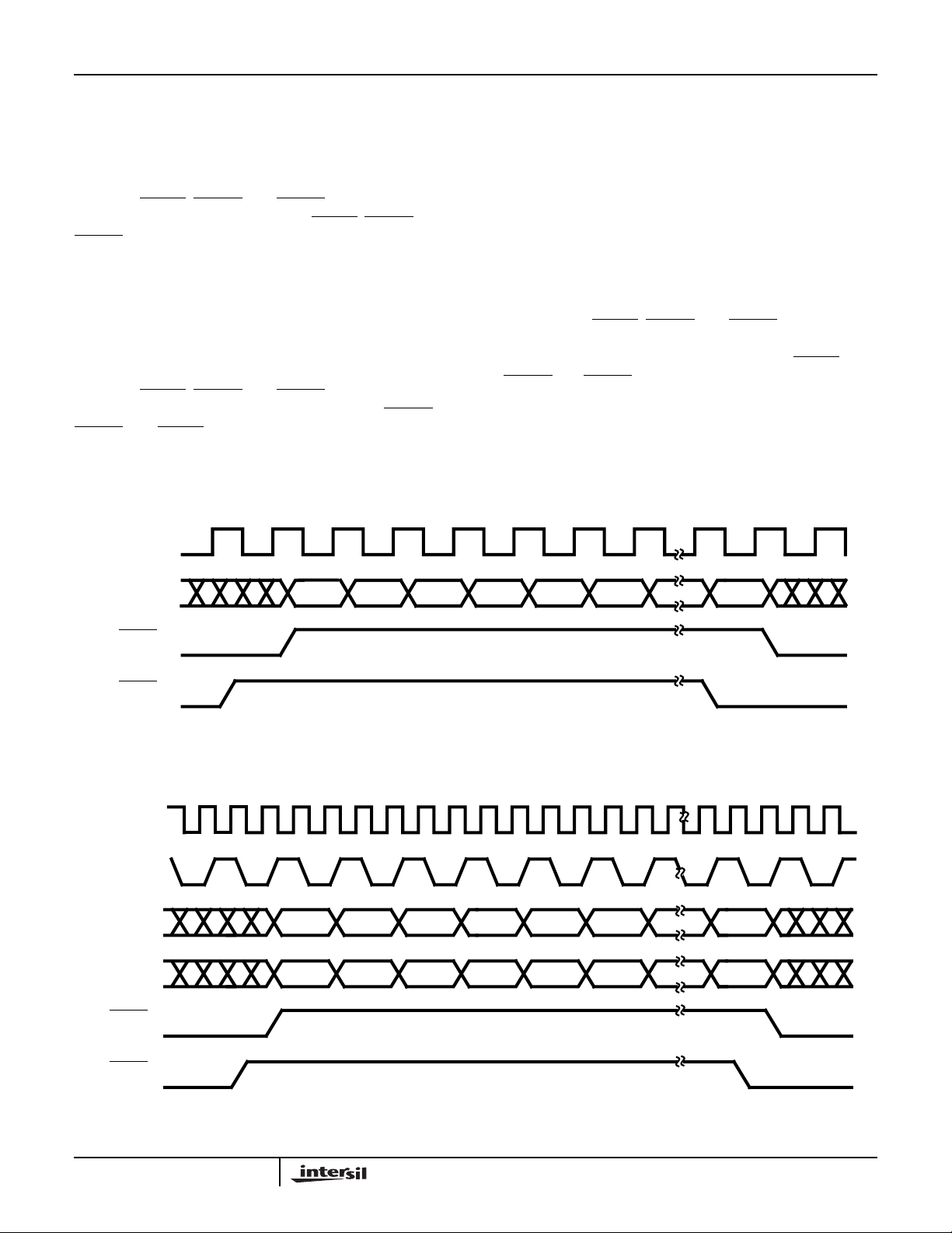
When 8-bit YCbCr format is selected, the data is latched on
each rising edge of CLK2. The pixel data must be [Cb Y Cr Y’
Cb Y Cr Y’ . . . ], with the first active data each scan line being
Cb data. The pixel input timing is shown in Figure 1.
As inputs,
each rising edge of CLK2. As outputs,
BLANK, HSYNC, and VSYNC are latched on
BLANK, HSYNC, and
VSYNC are output following the rising edge of CLK2. If the
CLK pin is configured as an input, it is ignored. If configured
as an output, it is one-half the CLK2 frequency.
16-Bit YCbCr Format
When 16-bit YCbCr format is selected, the pixel data is
latched on the rising edge of CLK2 while CLK is low. The
pixel input timing is shown in Figure 2.
As inputs,
rising edge of CLK2 while CLK is low. As outputs,
VSYNC, and BLANK are output following the rising edge of
CLK2 while CLK is high. In these modes of operation, CLK is
one-half the CLK2 frequency.
BLANK, HSYNC, and VSYNC are latched on the
HSYNC,
CLK2
8-Bit BT.656 Format
When BT.656 format is selected, data is latched on each
rising edge of CLK2. The pixel input timing is shown in
Figure 3. The figure shows the EAV code at the end of the
line. The format of the SAV and EAV codes are shown in
Table 3.
The BT.656 input may also include ancillary data to load the
VBI or RTCI data registers. The HMP817x will use the
ancillary data when enabled in the VBI data input and Timing
I/O registers. The ancillary data formats and the enable
registers are described later in this data sheet.
As inputs, the
ignored since all timing is derived from the EAV and SAV
sequences within the data stream. As outputs,
HSYNC and VSYNC are output following the rising edge of
CLK2. If the CLK pin is configured as an input, it is ignored. If
configured as an output, it is one-half the CLK2 frequency.
BLANK, HSYNC, and VSYNC pins are
BLANK,
P8-P15
BLANK
(INPUT)
BLANK
(OUTPUT)
CLK2
CLK
P8-P15
BLANK
(INPUT)
Cb 0 Y 0 Cr 0 Y 1 Cb 2 Y 2
FIGURE 1. PIXEL INPUT TIMING - 8-BIT YCBCR
Y 0Y 1Y 2Y 3Y 4Y 5
Cb 0 Cr 0 Cb 2 Cr 2 Cb 4 Cr 4P0-P7
Y N
Y N
Cr N-1
BLANK
(OUTPUT)
FIGURE 2. PIXEL INPUT TIMING - 16-BIT YCBCR
4
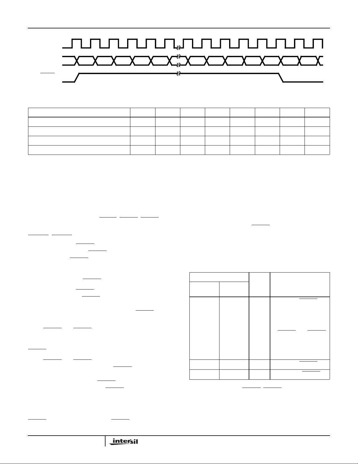
CLK2
HMP8170, HMP8171, HMP8172, HMP8173
P8-P15 "FF" "00"
BLANK
(OUTPUT)
Preamble Word 1 1 1 1 1 1 1 1 1
Preamble Word 2 0 0 0 0 0 0 0 0
Preamble Word 3 0 0 0 0 0 0 0 0
Status Word 1 F V H P3 P2 P1 P0
NOTES:
F: 0 = Field 1; 1 = Field 2
V: 0 = Active Line; 1 = Vertical Blanking
H: 0 = Start Active Video; 1 = End Active Video
P3 - P0: Protection bits; Ignored
Video Timing Control
The pixel input data and the output video timing of the
HMP817x are at 50 or 59.94 fields per second interlaced.
The timing is controlled by the
FIELD, and CLK2 pins.
HSYNC, VSYNC, and Field Timing
The leading edge of HSYNC indicates the beginning of a
horizontal sync interval. If
for about 4.7µs. If
least two CLK2 periods. The width of the analog horizontal
sync tip is determined from the video standard and does not
depend on the width of
The leading edge of VSYNC indicates the beginning of a
vertical sync interval. If
3 scan lines in (MM) NTSC and (M, N) PAL modes or 2.5
scan lines in (B, D, G, H, I, NC) PAL modes. If
Cb 2 Y 2 Cr 2 Y 3 Cb 4 Y 4
FIGURE 3. PIXEL INPUT TIMING - BT.656
TABLE 3. BT.656 EAV AND SAV SEQUENCES
PIXEL INPUT P15 P14 P13 P12 P11 P10 P9 P8
"00" EAV "10" "10""80"
resets its vertical half-line counter to the value specified by
the field control register. This allows the input and output
syncs to be offset, although the data must still be aligned.
BLANK, HSYNC, VSYNC,
The FIELD signal is always an output and changes state
near each leading edge of
VSYNC. The delay between the
syncs and FIELD depends on the encoder’s operating mode
as summarized in Table 4. In modes in which the encoder
uses CLK to gate its inputs and outputs, the FIELD signal
HSYNC is an output, it is asserted
may be delayed 0-12 additional CLK2 periods.
HSYNC is an input, it must be active for at
TABLE 4. FIELD OUTPUT TIMING
HSYNC.
VSYNC is an output, it is asserted for
OPERATING MODE
SYNC I/O
DIRECTION
BLANK I/O
DIRECTION
CLK2
DELAY COMMENTS
Input Input 148 FIELD lags VSYNC
switching from odd to
VSYNC is an
even.
input, it must be asserted for at least two CLK2 periods.
FIELD lags the earlier
When
HSYNC and VSYNC are configured as outputs, their
leading edges will occur simultaneously at the start of an
odd field. At the start of an even field, the leading edge of
VSYNC occurs in the middle of the line.
When HSYNC and VSYNC are configured as inputs, the
HMP817x provides a programmable
HSYNC window for
determining FIELD. The window is specified with respect to
the leading or trailing edge of
in the field control register.When
VSYNC. The edge is selected
HSYNC is found inside the
window, then the encoder sets FIELD to the value specified
in the field control register.
The HMP817x provides programmable timing for the
VSYNC input. At the active edge of VSYNC, the encoder
Input Output 138 FIELD lags
Output Don’tCare 32 FIELD leads
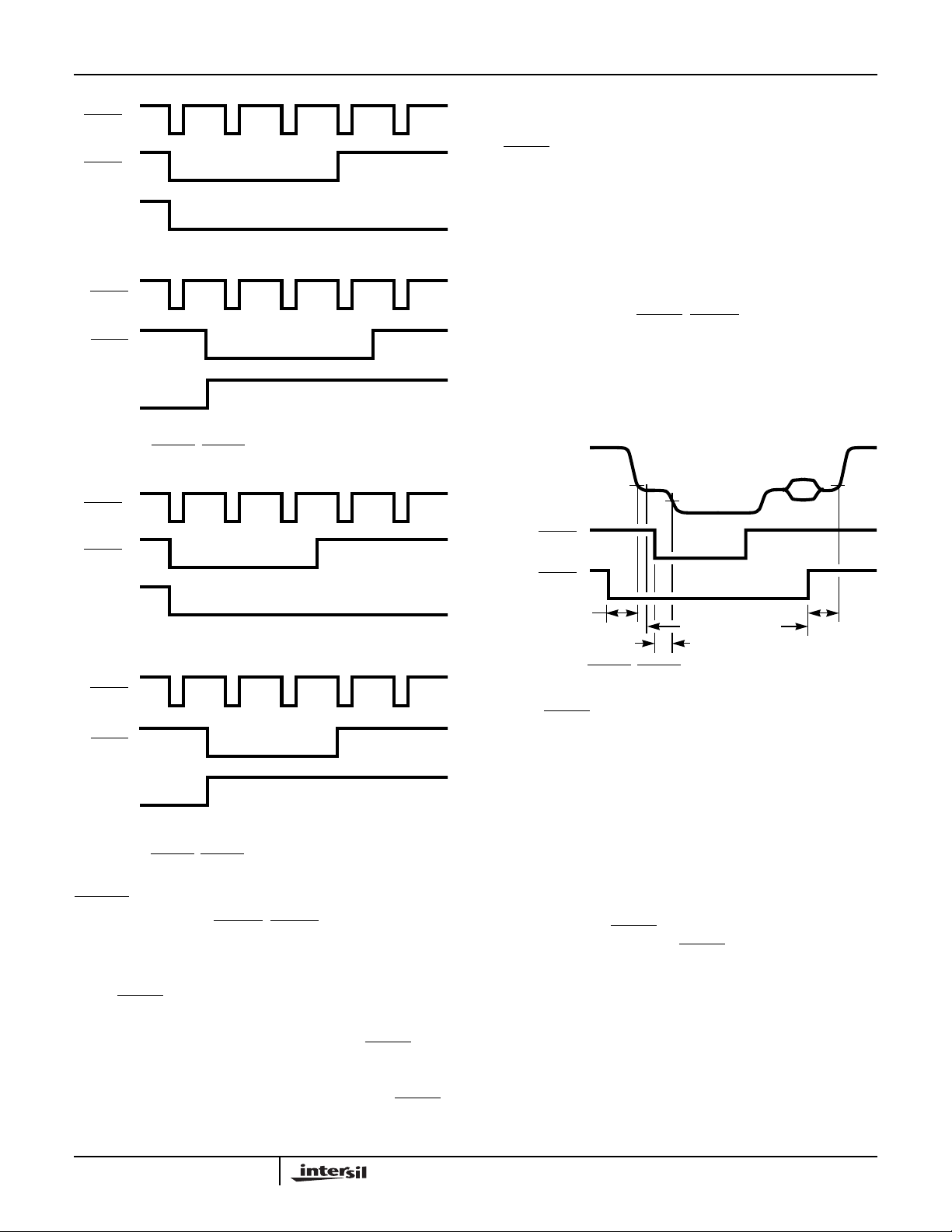
Figure 4 illustrates the
HSYNC, VSYNC, and FIELD general
timing for (M) NTSC and (M, N) PAL. Figure 5 illustrates the
general timing for (B, D, G, H, I, NC) PAL. In the figures, all
the signals are shown active low (their reset state), and
FIELD is low during odd fields.
of
VSYNC and HSYNC
when syncs are aligned
when switching from
even to odd.
VSYNC.
VSYNC.
5
HSYNC
VSYNC
HMP8170, HMP8171, HMP8172, HMP8173
There must be an even number of active and total pixels per
line. In the 8-bit YCbCr modes, the number of active and
total pixels per line must be a multiple of four. Note that if
BLANK is an output, half-line blanking on the output video
cannot be done.
FIELD
FIGURE 4A. BEGINNING AN ODD FIELD
HSYNC
VSYNC
FIELD
FIGURE 4B. BEGINNING AN EVEN FIELD
FIGURE 4. HSYNC, VSYNC, AND FIELD TIMING FOR
(M) NTSC AND (M, N) PAL
HSYNC
VSYNC
FIELD
FIGURE 5A. BEGINNING AN ODD FIELD
HSYNC
VSYNC
FIELD
FIGURE 5B. BEGINNING AN EVEN FIELD
FIGURE 5.
HSYNC, VSYNC, AND FIELD TIMING FOR
(B, D, G, H, I, NC) PAL
BLANK Timing
The encoder uses the HSYNC, VSYNC, FIELD signals to
generate a standard composite video waveform with no
active video (black burst). The signal includes only sync tips,
color burst, and optionally, a 7.5 IRE blanking setup. Based
on the
BLANK signal, the encoder adds the pixel input data
to the video waveform.
The encoder ignores the pixel input data when
asserted. Instead of the input data, the encoder generates
the blanking level. The encoder also ignores the pixel inputs
when generating VBI data on a specific line, even if
is negated.
BLANK is
BLANK
The HMP817x never adds a 7.5 IRE blanking setup during
the active line time on scan lines 1-21 and 263-284 for (M)
NTSC,scan lines 523-18 and 260-281 for (M) PAL, and scan
lines 623-22 and 311-335 for (B, D,G, H, I, N) PAL, allowing
the generation of video test signals, timecode, and other
information by controlling the pixel inputs appropriately.
The relative timing of
BLANK, HSYNC, and the output video
depends on the blanking and sync I/O directions. The typical
timing relation is shown in Figure 6. The delays which vary
with operating mode are indicated. The width of the
composite sync tip and the location and duration of the color
burst are fixed based on the video format.
.
COMPOSITE
VIDEO OUT
HSYNC
BLANK
DATA PIPE
DELAY
FIGURE 6. HSYNC, BLANK, AND OUTPUT VIDEO TIMING,
NORMAL MODE
START H BLANK
SYNC DELAY
When BLANK is an output, the encoder asserts it during the
inactive portions of active scan lines (horizontal blanking)
and for all of each inactive scan line (vertical blanking). The
inactive scan lines blanked each field are determined by the
start_v_blank and end_v_blank registers. The inactive
portion of active scan lines is determined by the
start_h_blank and end_h_blank registers.
The zero count for horizontal blanking is 32 CLK2 cycles
before the 50% point of the composite sync. From this zero
point, the HMP817x counts every other CLK2 cycle. When
the count reaches the value in the start_h_blank register, the
encoder negates
in the end_h_blank register,
BLANK. When the count reaches the value
BLANK is asserted. There may
be an additional 0-3 CLK2 delays in modes which use CLK.
The data pipeline delay through the HMP817x is 26 CLK2
cycles. In operating modes which use CLK to gate the
inputs into the encoder, the delay may be an additional 0-7
CLK2 cycles. The delay from BLANK to the start or end of
active video is an additional one-half CLK cycle when the
blank timing select bit is cleared. The active video may also
appear to end early or start late since the HMP817x
controls the blanking edge rates.
6
PIXELS PER LINE HBLANK REGISTER VALUES VBLANK REGISTER VALUES
VIDEO STANDARD
RECTANGULAR PIXELS (BT.601)
HMP8170, HMP8171, HMP8172, HMP8173
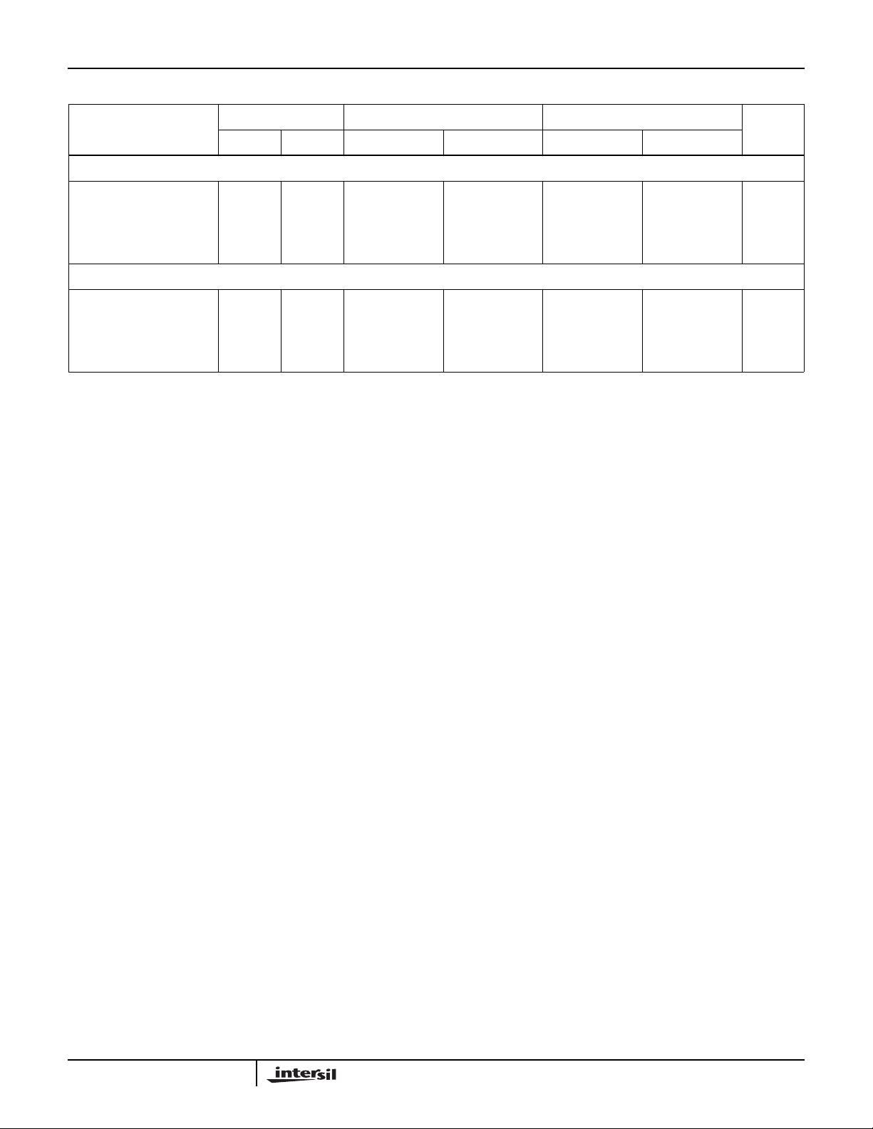
TABLE 5. TYPICAL VIDEO TIMING PARAMETERS
CLK2
(MHz)TOTAL ACTIVE START END START END
(M) NTSC
(B, D, G, H, I) PAL
(M) PAL
(N) PAL
(NC) PAL
SQUARE PIXELS
(M) NTSC
(B, D, G, H, I) PAL
(M) PAL
(N) PAL
(NC) PAL
858
864
858
864
864
780
944
780
944
944
720
720
720
720
720
640
768
640
768
768
842 (0x34a)
853 (0x355)
842 (0x34a)
853 (0x355)
853 (0x355)
758 (0x2f6)
923 (0x39b)
758 (0x2f6)
923 (0x39b)
923 (0x39b)
The delay from the active edge of HSYNC to the 50% point of
the composite sync is 4-39 CLK2 cycles depending on the
HMP817x operating mode. The delay is shortest when the
encoder is the timing master; it is longest when in slave mode.
CLK2 Input Timing
The CLK2 input clocks all of the HMP817x, including its
video timing counters. For proper operation, all of the
HMP817x inputs must be synchronous with CLK2. The
frequency of CLK2 depends on the device’s operating mode
and the total number of pixels per line. The standard clock
frequencies are shown in Table 5.
Note that the color subcarrier is derived from the CLK2 input.
Any jitter on CLK2 will be transferred to the color subcarrier,
resulting in color changes. Just 400ps of jitter on CLK2
causes up to a 1 degree color subcarrier phase shift. Thus,
CLK2 should be derived from a stable clock source, such as a
crystal. The use of a PLL to generate CLK2 is not
recommended.
122 (0x7a)
133 (0x85)
122 (0x7a)
133 (0x85)
133 (0x85)
118 (0x76)
155 (0x9b)
118 (0x76)
155 (0x9b)
155 (0x9b)
259 (0x103)
310 (0x136)
259 (0x103)
309 (0x135)
310 (0x136)
259 (0x103)
310 (0x136)
259 (0x103)
309 (0x135)
310 (0x136)
19 (0x13)
22 (0x16)
19 (0x13)
21 (0x15)
22 (0x16)
19 (0x13)
22 (0x16)
19 (0x13)
21 (0x15)
22 (0x16)
27.0
27.0
27.0
27.0
27.0
24.54
29.5
24.54
29.5
29.5
Video Processing
Upsampling
The encoder begins the video processing with the pixel input
data. It converts the 4:2:2 YCbCr data to 4:4:4 data. The
conversion is done by 2x upsampling the Cb and Cr data.
The CbCr upsampling function uses linear interpolation. The
HMP817x then upsamples the 4:4:4 data to generate 8:8:8
data. Again, the encoder uses linear interpolation for the
upsampling.
Horizontal Filtering
Unless disabled, the HMP817x lowpass filters the Y data to
6.0MHz. Lowpass filtering Y removes any aliasing artifacts
due to the upsampling process, and simplifies the analog
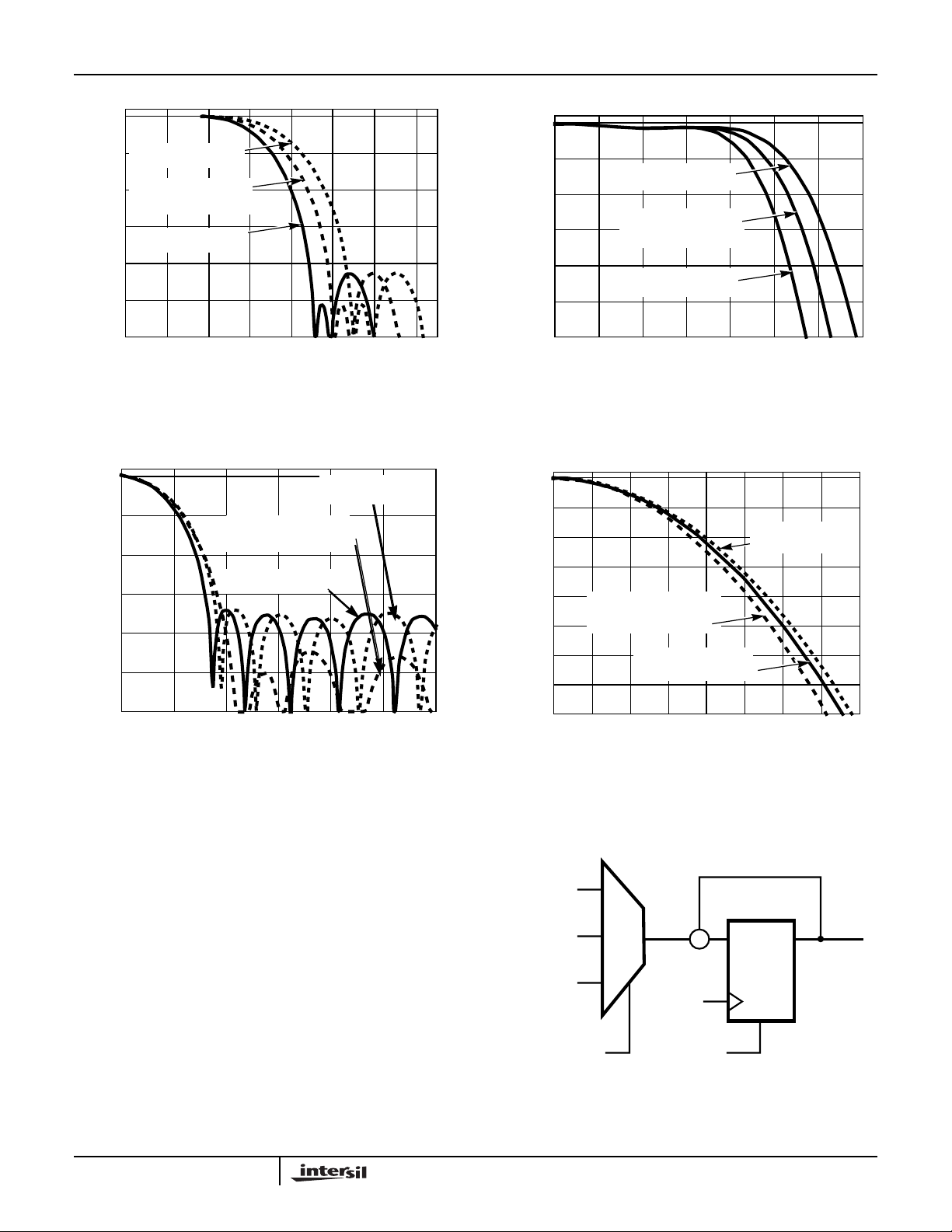
output filters. The Y 6.0MHz lowpass filter response is
shown in Figure 7. At this point, the HMP817x also scales
the Y data to generate the proper output levels for the
various video standards.
The HMP817x lowpass filters the Cb and Cr data to 1.3MHz
prior to modulation. The lowpass filtering removes any
aliasing artifacts due to the upsampling process (simplifying
the analog output filters) and also properly bandwidth-limits
Cb and Cr prior to modulation. The chrominance filtering is
not optional like luminance filtering. The Cb and Cr 1.3MHz
lowpass filter response is shown in Figure 8.
7
HMP8170, HMP8171, HMP8172, HMP8173
ATTENUATION (dB)
.
ATTENUATION (dB)
0
PAL SQUARE PIXEL
-10
CLK2 = 29.50MHz
NTSC OR PAL
-20
RECTANGULAR PIXEL
CLK2 = 27.00MHz
-30
NTSC SQUARE PIXEL
CLK2 = 24.54MHz
-40
-50
-60
0 2 4 6 8 10 12 14
FREQUENCY (MHz)
FIGURE 7A. FULL SPECTRUM FIGURE 7B. PASS BAND
FIGURE 7. Y LOWPASS FILTER RESPONSE
-10
-20
-30
-40
-50
0
NTSC OR PAL
RECTANGULAR PIXEL
CLK2 = 27.00MHz
NTSC SQUARE PIXEL
CLK2 = 24.54MHz
PAL SQUARE PIXEL
CLK2 = 29.50MHz
0
-0.5
-1.0
-1.5
-2.0
ATTENUATION (dB)
-2.5
-3.0
012345 67
0
-0.5
-1.0
-1.5
-2.0
-2.5
ATTENUATION (dB)
-3.0
-3.5
PAL SQUARE PIXEL
CLK2 = 29.50MHz
NTSC OR PAL
RECTANGULAR PIXEL
CLK2 = 27.00MHz
NTSC SQUARE PIXEL
CLK2 = 24.54MHz
FREQUENCY (MHz)
NTSC OR PAL
RECTANGULAR PIXEL
CLK2 = 27.00MHz
NTSC SQUARE PIXEL
CLK2 = 24.54MHz
PAL SQUARE PIXEL
CLK2 = 29.50MHz
-60
024681012
FREQUENCY (MHz)
FIGURE 8A. FULL SPECTRUM FIGURE 8B. PASS BAND
FIGURE 8. Cb AND Cr LOWPASS FILTER RESPONSE
Color Subcarrier Generation
The HMP817x uses a numerically controlled oscillator
(NCO) clocked by CLK2 and a sine look up ROM to generate
the color subcarrier. As shown in Figure 9, the phase
increment value (PHINC) of the NCO may come from the
encoder’s internal look up table, BT.656 ancillary data, or a
control register. The PHINC source is selected in timing I/O
register 2.
-4.0
0 0.2 0.4 0.6 0.8 1.0 1.2
FREQUENCY (MHz)
.
INTERNAL
BT.656
2
I
SELECT
C
PHINC
PHINC
+
CLK2
NCO RESET
Q
D
FIGURE 9. COLOR SUBCARRIER GENERATION NCO.
1.4 1.6
PHINT
8

HMP8170, HMP8171, HMP8172, HMP8173
The MSBs of the accumulated phase value (PHINT) are
used to address the encoder’s sine look up ROM. The sine
values from the ROM are pre-scaled to generate the proper
levelsforthe various video standards. Prescaling outside the
CbCr data path minimizes color processing artifacts. The
HMP817x modulates the filtered 8:8:8 chrominance data
with the synthesized subcarrier.
The SCH phase is 0 degrees after reset but then changes
monotonically over time due to residue in the NCO . In an ideal
system, zero SCH phase would be maintained fore v er. In
reality, this is impossible to achievedue to pixel clock frequency
tolerancesand digital rounding errors. When thePHINC source
is BT.656 data, the SCH phase reset should be disabled.
If enabled, the HMP817x resets the NCO periodically to
avoidan accumulation of SCH phase error.The reset occurs
at the beginning of each field to burst phase sequence. The
sequence repeats every 4 fields for NTSC or 8 fields for PAL.
Resetting the SCH phase every four fields (NTSC) or eight
fields (PAL) avoids the accumulation of SCH phase error at
the expense of requiring any NTSC/PAL decoder after the
encoder be able to handle very minor “jumps” (up to 2
degrees) in the SCH phase at the beginning of each fourfield or eight-field sequence. Most NTSC/PAL decoders are
able to handle this due to video editing requirements.
Composite Video Limiting
The HMP817x adds the luminance and modulated
chrominance together with the sync, color burst, and
optional blanking pedestal to form the composite video data.
If enabled in the video processing register,the encoder limits
the active video so that it is always greater than one-eighth
of full scale. This corresponds to approximately one-half the
sync height. This allows the generation of “safe” video in the
event non-standard YCbCr values are input to the device.
Controlled Edges
The NTSC and PAL video standards specify edge rates and
rise and fall times for portions of the video waveform. The
HMP817x automatically implements controlled edge rates
and rise and fall times on these edges:
1. Analog Horizontal Sync (Rising and Falling Edges)
2. Analog Vertical Sync Interval (Rising and Falling Edges)
3. Color Burst Envelope
4. Blanking of Analog Active Video
5. Closed Captioning Information
6. WSS Information
7. Teletext Information
“Sliced” VBI Data
The HMP817x generates three types of vertical blanking
interval data: closed captioning, widescreen signalling, and
teletext data. The data is generated on the scan lines
specified by the selected output video standard which are
enabled in the VBI data control register. During scan lines
with VBI data, the pixel inputs are ignored.
Closed Captioning (CC)
The HMP817x captioning data output includes clock run-in and
start bits followed by the captioning data. During closed
captioning encoding, the pixel inputs are ignored on the scan
lines containing captioning information.
The HMP817x has two 16-bit registers containing the
captioning information. Each 16-bit register is organized as
two cascaded 8-bit registers. One 16-bit register (caption 21)
is read out serially during line 18, 21 or 22; the other 16-bit
register (WSS 284) is read out serially during line 281, 284
or 335. The data registers are shifted out LSB first.
The captioning output level is 50 IRE for a logic 1 and 0 IRE
for a logic 0. All transitions between levels are controlled to
have a raised-cosine shape. The rise or fall time of any
transition is 240-288ns.
The caption data registers may be loaded via the I
or as BT.656 ancillary data. Table 6 illustrates the format of the
caption data as BT.656 ancillary data. The transfer should
occur only once per field before the start of the SAV sequence
of the line containing the captioning output.
When written via the I
in any order but both must be written within one frame time
for proper operation. If the registers are not updated, the
encoder resends the previously loaded values.
The HMP817x provides a write status bit for each captioning
line. The encoder clears the write status bit to ‘0’ when
captioning is enabled and both bytes of the captioning data
register have been written. The encoder sets the write status
bit to ‘1’ after it outputs the data, indicating the registers are
ready to receive new data.
Captioning information may be enabled for either line, both
lines, or no lines. The captioning modes are summarized in
Table 7.
2
C interface, the bytes may be written
2
C interface
9

HMP8170, HMP8171, HMP8172, HMP8173
TABLE 6. BT.656 ANCILLARY DATA FORMAT FOR CLOSED CAPTIONING DATA
PIXEL INPUT P15 P14 P13 P12 P11 P10 P9 P8
Preamble 1 0 0 0 0 0 0 0 0
Preamble 2 1 1 1 1 1 1 1 1
Preamble 3 1 1 1 1 1 1 1 1
Data ID ep# ep 1 1 0 0 0 Line
Data Block Number ep# ep 0 0 0 0 0 1
Data Word Count ep# ep 0 0 0 0 0 1
Caption Register Byte 3 ep# ep 0 0 bit 15 bit 14 bit 13 bit 12
Caption Register Byte 1 ep# ep 0 0 bit 11 bit 10 bit 9 bit 8
Caption Register Byte 1 ep# ep 0 0 bit 7 bit 6 bit 5 bit 4
Caption Register Byte 0 ep# ep 0 0 bit 3 bit 2 bit 1 bit 0
CRC P14# X X X X X X X
NOTES:
The even parity (EP and EP#) bits are ignored.
Line = Data Register Select: 0 = Line 21; 1 = 284.
X = Don’t Care.
TABLE 7. CLOSED CAPTIONING MODES
CLOSED
CAPTIONING
ENABLE BITS OUTPUT LINE(S)
00 None Ignored Ignored Always 1 Always 1
01 21 (NTSC)
18 (M PAL)
22 (Other PAL)
10 284 (NTSC)
281 (M PAL)
335 (Other PAL)
11 21, 284 (NTSC)
18, 281 (M PAL)
22, 335 (Other PAL)
CAPTIONING REGISTER WRITE STATUS BIT
284A
284B
Ignored Caption Data Always 1 0 = Loaded
Caption Data Ignored 0 = Loaded
Caption Data Caption Data 0 = Loaded
21A
21B 284 21
1 = Output
1 = Output
1 = Output
Always 1
0 = Loaded
1 = Output
Widescreen Signalling (WSS)
The HMP817x WSS data output includes clock run-in and
start codes followed by the WSS data. For NTSC operation,
the WSS data is followed by six bits of CRC data.
The HMP817x has two 14-bit registers containing the WSS
information and two 6-bit registers containing the WSS CRC
data. Each 14-bit register is organized as a 6-bit register
cascaded with an 8-bit one. One 14-bit register (WSS 20) is
read out serially during line 17, 20 or 23; the other 14-bit
register (caption 283) is read out serially during line 280, 283
or 336. The data registers are shifted out LSB first.
The WSS output level depends on the video f ormat. F or
NTSC operation (EIAJ CPX-1204), the WSS output level is 70
IRE for a logic 1 and 0 IRE for a logic 0. All transitions
between levels are controlled to have a raised-cosine shape
with a rise or fall time of 240ns. For PAL operation (ITU-R
BT.1119), the WSS output level is 71.5 IRE for a logic 1 and 0
IRE for a logic 0. All transitions between le vels are controlled
to havea raised-cosine shape with a rise or fall time of 118ns.
10
The WSS data registers may be loaded via the I
2
C interface
or as BT.656 ancillary data. Table 8 illustrates the format of
the WSS data as BT.656 ancillary data. The transfer should
occur only once per field before the start of the SAV
sequence of the line containing the WSS output.
When written via the I
2
C interface, the bytes may be written
in any order but all three bytes of each enabled line must be
written within one frame time for proper operation. If the
registers are not updated, the encoder resends the
previously loaded values.
The HMP817x provides a write status bit for each WSS line.
The encoder clears the write status bit to ‘0’ when WSS is
enabled and all bytes of the WSS data register hav e been
written. The encoder sets the write status bit to ‘1’ after it
outputs the data, indicating the registers are ready to receive
new data.
WSS information may be enabled for either line, both lines,
or no lines. The WSS modes are summarized in Table 9.
 Loading...