Intersil Corporation HMP8154, HMP8156A Datasheet
HMP8154, HMP8156A
Data Sheet October 1998 File Number 4343.3
NTSC/PAL Encoders
The HMP8154 and HMP8156A NTSC and PAL encoders
are designed for use in systems requiring the generation of
high-quality NTSC and PAL video from digital image data.
YCbCr or RGB digital video data drive the P0-P23 inputs.
Overlay inputs are processed and the data is 2x upsampled.
The Y data is optionally lowpass filtered to 6MHz and drives
the Y analog output. Cb and Cr are each lowpass filtered to
1.3MHz, quadrature modulated, and summed. The result
drives the C analog output. The digital Y and C data are also
added together and drive the two composite analog outputs.
The YCbCr data may also be converted to RGB data to drive
the DACs, allowing support for analog component RGB and
the European SCART connector.
The DACs can drive doubly-terminated (37.5Ω) lines, and
run at a 2x oversampling rate to simplify the analog output
filter requirements. AnyunusedDACs maybepowereddown
to reduce power consumption.
Ordering Information
TEMP.
PART NUMBER
HMP8154CN 0 to 70 64 Ld PQFP Q64.14x14
HMP8156ACN 0 to 70 64 Ld PQFP Q64.14x14
HMP8154EVAL1
HMP8156EVAL1
RANGE (oC) PACKAGE PKG. NO.
Daughter/Stand-Alone Card Evaluation
Platform (Note)
Features
• (M) NTSC and (B, D, G, H, I, M, N, CN) PAL Operation
• ITU-R BT.601 and Square Pixel Operation
• Digital Input Formats
- 4:2:2 YCbCr
- 8-Bit or 16-Bit
- 4:4:4 RGB
- 16-Bit (5, 6, 5) or 24-Bit (8, 8, 8)
- Linear or Gamma-Corrected
- 8-Bit BT.656
• Overlay Mixing
- 7 Colors
- Internal, External, or Hard Mixing Control
• Analog Output Formats
- Y/C + Two Composite
- RGB + Composite (SCART)
• Flexible Video Timing Control
- Timing Master or Slave
- Programmable Input Sync Timing
- Selectable Polarity on Each Control Signal
- Programmable Blank Output Timing
- Field Output
• Closed Caption Encoding for NTSC and PAL
• 2x Upscaling of SIF Video
• Three Line Vertical Flicker Filter
(HMP8154 only)
HMP8156EVAL2 Frame Grabber Evaluation Platform (Note)
NOTE: Described in the Applications Section
1
CAUTION: These devices are sensitive to electrostatic discharge; follow proper IC Handling Procedures.
• Four 2x Oversampling, 10-Bit DACs with Power Down
2
•I
C Interface
• Verilog Models Available
Applications
• Multimedia PCs
• Video Conferencing
• Video Editing
• Related Products
- NTSC/PAL Encoders:
HMP8170-HMP8173
- HMP8190/91
- NTSC/PAL Decoders:
HMP8112A, HMP8115, HMP8116, HMP8130/31
http://www.intersil.com or 407-727-9207 | Copyright © Intersil Corporation 1999
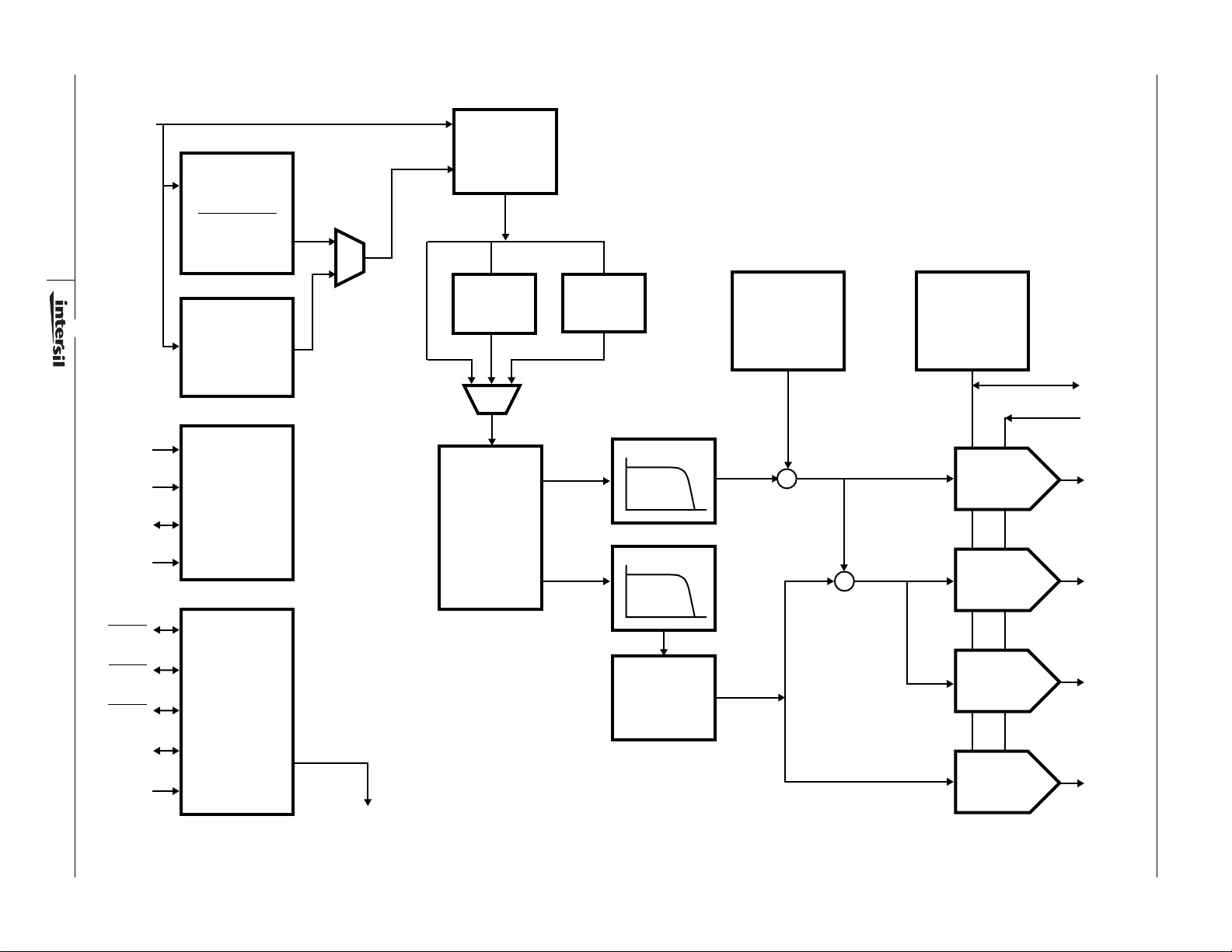
Functional Block Diagram
P0 - P23
OPTIONAL
GAMMA
CORRECTION
COLOR
SPACE
2
CONVERSION
Y/Cb/Cr
4:4:4
(2:2:2 SIF)
OVERLAY
PROCESSING
SA
SCL
SDA
RESET
HSYNC
VSYNC
BLANK
CLK
4:2:2 TO
4:4:4 SAMPLE
CONVERSION
HOST
INTERFACE
VIDEO
TIMING
CONTROL
2X
UPSCALING
(SIF MODE)
2 X
UPSAMPLE
4:4:4
TO
8:8:8
(HMP8154
Y
Cb/Cr
FLICKER
FILTER
ONLY)
(OPTIONAL)
LP FILTER
LP FILTER
CHROMA
MODULATION
CLOSED
CAPTIONING
PROCESSING
∑
INTERNAL
1.225V
REFERENCE
VREF
FS
ADJUST
DAC
∑
DAC
DAC
Y/G
NTSC/
PAL 1
NTSC/
PAL 2/
R
CLK2
FIELD
DAC
C/B

HMP8154, HMP8156A
Functional Operation
The HMP8154 and HMP8156A are fully integrated digital
encoders. Either accepts digital video input data and
generates four analog video output signals. The input data
format is selectable and includes YCbCr, RGB, and overlay
data. The outputs are configurable to be either two
composite video signals and Y/C (S-Video) or one
composite and component RGB video.
The HMP8154/HMP8156A accepts pixel data in one of
several formats and transforms it into 4:4:4 sampled
luminance and chrominance (YCbCr) data. If enabled, the
encoder also mixes overlay data with the input data. The
encoder then interpolates the YCbCr data to twice the pixel
rate and low pass filters it to match the bandwidth of the
video output format. If enabled, the encoder also adds
Closed Captioning information to the Y data. At the same
time, the encoder modulates the chrominance data with a
digitally synthesized subcarrier. Finally, the encoder outputs
luminance, chrominance, and their sum as analog signals
using 10-bit D/A converters.
The HMP8154/HMP8156A provides operating modes to
support all versions of the NTSC and PAL standards and
accepts full and SIF size input data with rectangular (ITU-R
BT.601) and square pixel aspect ratios. It operates from a
single clock at twice the pixel clock rate determined by the
operating mode.
The HMP8154/HMP8156A’svideotimingcontrolisflexible.It
may operate as the master generating the system’s video
timing control signals or it may accept external timing
controls. The polarity of the timing controls and the number
of active pixels and lines are programmable.
The HMP8154 provides optional vertical flicker reduction.
When enabled, the encoder passes the pixel data after
overlay processing through a three line flicker filter.
Pixel Data Input Formats
The HMP8154 accepts pixel data via the P0-P23 input pins.
The definition of each pixel input pin is determined by the
input format selected in the input format register. The
definition for each mode is shown in Table 1.
YCbCr Pixel Data
The HMP8154/HMP8156A accepts 4:2:2 sampled YCbCr
input data. The luminance and color difference signals are
each 8 bits, scaled 0 to 255. The nominal range for Y is 16
(black) to 235 (white). Y values less than 16 are clamped to
16; values greater than 235 are processed normally. The
nominal range for Cb and Cr is 16 to 240 with 128
representing zero. Cb and Cr v alues outside their nominal
range are processed normally. Note that when converted to
the analog outputs, some combinations of YCbCr outside
their nominal ranges would generate a composite video signal
larger than the analog output limit. The composite signal will
be clipped but the S-video outputs (Y and C) will not be.
The color difference signals are time multiplexed into one
8-bit bus beginning with a Cb sample. The Y and CbCr
busses may be input in parallel (16-bit mode) or may be time
multiplexed and input as a single bus (8-bit mode). The
single bus may also contain SAV and EAV video timing
reference codes (BT.656 mode).
RGB Data
The HMP8154/HMP8156A accepts 4:4:4 sampled RGB
component video input data. The color signals may be
(8,8,8) for 24-bit mode or (5,6,5) for 16-bit mode. In 24-bit
mode, they are scaled 0 to 255, black to white. In 16-bit
mode, the encoder left shifts the input so that it has the same
scale as 24-bit input. The RGB data may be linear or gamma
corrected; if enabled, the encoder will gamma correct the
input data.
Overlay Data
The HMP8154/HMP8156A accepts 5 bits of pixel overlay
input data and combines it with the input pixeldata. The data
specifies an overlay color and the fractions of the new and
original colors to be summed.
Blue Screen Generation
In blue screen mode, the HMP8154/HMP8156A ignores the
pixel input data and generates a solid, blue screen. The
overlay inputs may be used to place information over the
blue screen.
Input Processing
Color Space Conversion
For linear RGB input formats, the encoder applies gammacorrection using a selectable gamma value of 1/2.2 or 1/2.8.
The gamma-corrected RGB data from either the correction
function in linear mode or the input port otherwise is
converted to 4:4:4 sampled YCbCr data.
For the YCbCr input formats, the encoder converts the 4:2:2
sampled data to 4:4:4 sampled data. The conversionis done
by 2x upsampling the Cb and Cr data. The upsampling
function uses linear interpolation.
Overlay Processing
The HMP8154/HMP8156A accepts overlay data via the
OL0-OL2, M0, and M1 pins. Overlay mixing is done using
the 4:4:4 YCbCr pixel data from the color space converter.
The YCbCr data following overlay processing is used as
input data by the video processing functions.
The OL0-OL2 inputs select the color to be mixed with the
pixel data. Overlay colors 1-7 are standard color bar colors.
Overlay color 0 is special and disables mixing on a pixel-bypixel basis. The overlay color palette is shown in Table 2.
3

PIN
NAME
P0
P1
P2
P3
P4
P5
P6
P7
P8
P9
P10
P11
P12
P13
P14
P15
P16
P17
P18
P19
P20
P21
P22
P23
16-BIT
4:2:2
YCBCR
Cb0, Cr0
Cb1, Cr1
Cb2, Cr2
Cb3, Cr3
Cb4, Cr4
Cb5, Cr5
Cb6, Cr6
Cb7, Cr7
Y0
Y1
Y2
Y3
Y4
Y5
Y6
Y7
HMP8154, HMP8156A
TABLE 1. PIXEL DATA INPUT FORMATS
8-BIT
4:2:2
YCBCR BT.656
Ignored B0
Y0, Cb0, Cr0
Y1, Cb1, Cr1
Y2, Cb2, Cr2
Y3, Cb3, Cr3
Y4, Cb4, Cr4
Y5, Cb5, Cr5
Y6, Cb6, Cr6
Y7, Cb7, Cr7
YCbCr Data,
SAV and EAV
Sequences
OL0
OL1
OL2
M0
M1
-
-
-
16-BIT
BLUE
SCREEN
Ignored G3
(5, 6, 5)
RGB
B1
B2
B3
B4
G0
G1
G2
G4
G5
R0
R1
R2
R3
R4
24-BIT
RGB
B0
B1
B2
B3
B4
B5
B6
B7
G0
G1
G2
G3
G4
G5
G6
G7
R0
R1
R2
R3
R4
R5
R6
R7
TABLE 2. OVERLAY COLOR PALETTE
OL2-OL0
000
001
010
011
100
101
110
111
COLOR
Pixel Data
75% Blue
75% Red
75% Magenta
75% Green
75% Cyan
75% Yellow
100% White
Note that overlay capability is not available when the 24-bit
RGB input format is used.
The encoder provides 4 methods for mixing the overlay data
with the pixel data: disabled, external mixing, internal mixing
and no mixing. The method used is selected in the input
format control register.
Overlay Mixing: Disabled
When overlay mixing is disabled, the OL0-OL2, M0, and M1
inputs are ignored and the pixel data is not changed.
Overlay Mixing: External
When external overlay mixing is selected, mixing of overlay
data and pixel data is controlled by the M1 and M0 inputs.
M1 and M0 indicate the mixing level between the pixel inputs
and the overlay inputs, on a pixel-by-pixel basis. M1 and M0
are ignored if OL2-OL0 = 000. Otherwise, they select the
percentage of each color to sum as shown in Table 3.
TABLE 3. OVERLAY MIXING FACTORS
M1, M0
00
01
10
11
% OVERLAY
COLOR
0
12.5
87.5
100
% PIXEL
COLOR
100
87.5
12.5
0
In external mixing mode, there is no minimum number of
pixels an overlay color or pixel color must be selected. The
mixing level may also vary at any rate.
Overlay Mixing: Internal
Mixing of overlay and pix el data ma y also be controlled
internally, and the M1 and M0 input pins are ignored. A
transition from pixel data to ov erla ys, from o v erla ys to pix el
data, or between different ov erlay colors triggers the mixing
function. An overlay color must be selected f or a minim um of
three pixels for proper overlay operation in this mode. Internal
overlaymixing should not be used with the BT .656input format.
When going from pixel to overlay data, mixing starts one
pixel before the selection of the overlay color (OL2-OL1 !=
000). The first pixel output before the overlay uses 12.5%
overlay color plus 87.5% pixel color. The next output is
aligned with the selection of the overlay color and uses
87.5% overlay color plus 12.5% pixel color. Additional
outputs use 100% overlay color.
When going from overlay to pixel data, mixing starts one
pixel before the selection of the pixel color (OL2-OL0 = 000).
4
HMP8154, HMP8156A
The last pixel output of the overlay uses 87.5% overlay color
plus 12.5% pixel color. The next output uses 12.5% overlay
color plus 87.5% pixel color. Additional outputs use 100%
pixel color.
When going from one overlay color to another, mixing
starts one pixel before the selection of the new overlay
color, and uses 12.5% new overlay color plus 87.5% old
overlay color. The next output is aligned with the selection
of the new overlay color and uses 87.5% new overlay color
plus 12.5% old overlay color. Additional outputs use 100%
new overlay color.
Overlay Mixing: No Mixing
With no overlay mixing selected, whenever the OL0-OL2
inputs are non-zero, the overlay color is displayed. The M0
and M1 inputs are ignored, and no internal mixing is done.
Essentially, this is a hard switch between overlay and pixel
data. In this mode, there is no minimum number of pixels an
overlay color or pixel color must be selected.
2X Upscaling Processing
Following overlay processing, 2X upscaling may optionally
be applied to the pixel data. In this mode, the
HMP8154/HMP8156A accepts NTSC (PAL) SIF resolution
video at 59.94 (50)
standard interlaced video with 262.5 (312.5) lines per field at
59.94 (50)
fields
SIF video to be upscaled to full resolution and recorded on a
VCR or displayed on a TV. SIP upscaling may be used to
simplify PC to TV applications.
The input pixel data rate is reduced by half when 2X
upscaling is enabled. The color space conversion generates,
and the overlay mixer uses, 2:2:2 YCbCr data instead of
4:4:4 data. For rectangular pixel NTSC and PAL video, the
input rate is 6.75MHz during the active portion of each line
instead of 13.5MHz. Example SIF input resolutions and
resulting output resolutions are shown in Table 4.
TABLE 4. TYPICAL RESOLUTIONS FOR 2X UPSCALING
INPUT ACTIVE
RESOLUTION
352 x 240
352 x 288
320 x 240
384 x 288
The HMP8154/HMP8156A performs horizontal 2X upscaling
by linear interpolation. The vertical scaling is done by line
duplication. For typical line duplication, the same frame of
SIF pixel input data is used for both the odd and even fields.
Note that a frame of SIF size input has about the same
number of lines as a field of full size input.
After 2X upscaling, the input is 4:4:4 YCbCr data ready for
video processing. Flicker filtering is not available when 2X
upscaling is enabled.
frames
per second and generates
per second. This mode of operation allows
OUTPUT ACTIVE
RESOLUTION
704 x 480
704 x 576
640 x 480
768 x 576
Flicker Filter Processing
Following overlay processing, vertical flicker filtering may
optionally be applied to the pixel data by the HMP8154. The
HMP8156A does not provide flicker filter capability. In flicker
filter mode, the HMP8154 accepts non-interlaced NTSC
(PAL) full resolution video with 525 (625) lines per frame at
59.94 (50)
frames
per second. It generates standard
interlaced video with 262.5 (312.5) lines per field at 59.94
(50)
fields
per second.
Each frame of non-interlaced video is vertically low pass
filtered and used to generate either an odd or even field of
video. This mode of operation reduces flickering caused by
image details that are less than two pixels high.
Since an entire frame of input is used to generate one field of
output, the input pixel data rate is doubled when the flic ker
filter is enabled. The encoder must receive two lines of data
during each line time. For rectangular pixel NTSC and PAL
video, the input rate is 27.0MHz during the active portion of
each line instead of 13.5MHz. Because of the high input data
rate, 8-bit YCbCr and BT.656 input formats and 2X upscaling
of SIF input may not be used when the flicker filter is enabled.
The HMP8154 uses internal line stores and a 3 tap FIR filter
to reduce flickering. The filter coefficients are 0.25, 0.5, and
0.25. At the start and end of each field, the coefficients are
modified to compensate for the insufficient number of lines
available for processing.
When filtering is enabled, there is an additional two line time
delay through the encoder. After flicker filtering, the input is
4:4:4 YCbCr data ready for video processing. 2X upscaling
is not available when the flicker filter is enabled.
Pixel Input and Control Signal Timing
The pixel input timing and the video control signal
input/output timing of the HMP8154/HMP8156A depend on
the part’s operating mode. The periods when the encoder
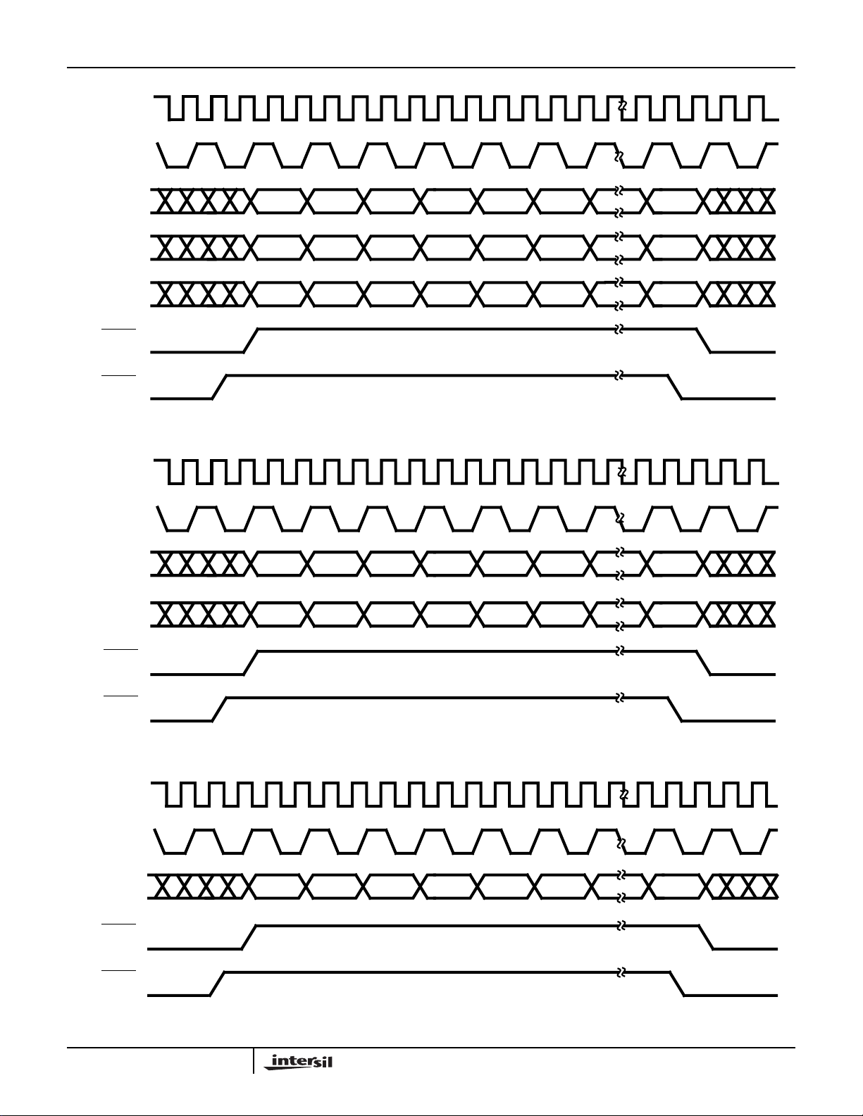
samples its inputs and generates its outputs are
summarized in Table 5.
Figures 1-12 show the timing of CLK, CLK2,
pixel and overlay input data with respect to each other.
BLANK may be an input or an output; the figures show both.
When it is an input,
BLANK must arrive coincident with the
pixel and overlay input data; all are sampled at the same time.
When
BLANK is an output, its timing with respect to the pixel
and overlay inputs depends on the blank timing select bit in the
timing_I/O_1 register. If the bit is cleared, the
HMP8154/HMP8156Adeasserts
BLANKoneCLKcyclebef ore
it samples the pixel and overla y inputs . As shown in the timing
figures, the encoder samples the inputs 1-7 CLK2 periods after
negating
BLANK, depending on the operating mode.
If the bit is set, the encoder deasserts BLANK during the
same CLK cycle in which it samples the input data. In effect,
the input data must arrive one CLK cycle earlier than when
the bit is cleared. This mode is not shown in the figures.
BLANK, and the
5

HMP8154, HMP8156A
TABLE 5. PIXEL INPUT AND CONTROL SIGNAL I/O TIMING
INPUT PORT SAMPLING VIDEO TIMING CONTROL (NOTE 2) CLK FREQUENCY
INPUT FORMAT
8-Bit YCbCr Norm Every rising edge
16-Bit YCbCr,
16-Bit RGB,
or
24-Bit RGB
BT.656 Norm Every rising edge
NOTES:
1. Encoder operatingmodes:
Norm = Full size input, Flicker filter disabled.
2X = SIF size input, Flicker filter disabled.
FF = Full size input, Flicker filter enabled.
(2X upscaling and flicker filtering are mutually exclusive.)
2. Video timingcontrolsignals includeHSYNC, VSYNC,BLANKand FIELD.Thesync andblanking I/Odirectionsare independent;FIELDis always
an output.
MODE
2X Rising edge of
FF Not Available
Norm Rising edge of CLK2 when CLK is low Rising edge of
2X 2nd rising edge of CLK2 when CLK is low Either rising CLK2
FF Every rising edge
2X Not Available
FF Not Available
PIXEL DATA OVERLAY DATA INPUT SAMPLE OUTPUT ON INPUT OUTPUT
(NOTE 1)
of CLK2
CLK2 when CLK is
low.
of CLK2
of CLK2
Same edge that
latches Y
Same edge that
latches Y data
Same edge that
latches Y
Same edge that
latches Y
Every rising edge
of CLK2
Rising edge of
CLK2 when CLK is
low.
Every rising edge
of CLK2
Not Allowed Any rising edge of
Any rising edge of
CLK2
Rising edge of
CLK2 when CLK is
high.
CLK2 when CLK is
high.
edge when CLK is
high
Any rising edge of
CLK2
CLK2
Ignored One-half
CLK2
One-half CLK2
One-half CLK2
One-fourth CLK2
Ignored One-half
CLK2
Ignored One-half
CLK2
Normal 8-Bit YCbCr Format
When 8-bit YCbCr format is selected and 2X upscaling or
flicker filtering is not enabled, the data is latched on each
rising edge of CLK2. The pixel data must be [Cb Y Cr Y’ Cb Y
Cr Y’ . . . ], with the first active data each scan line being Cb
data. Overlay data is latched when the Y input data is latched.
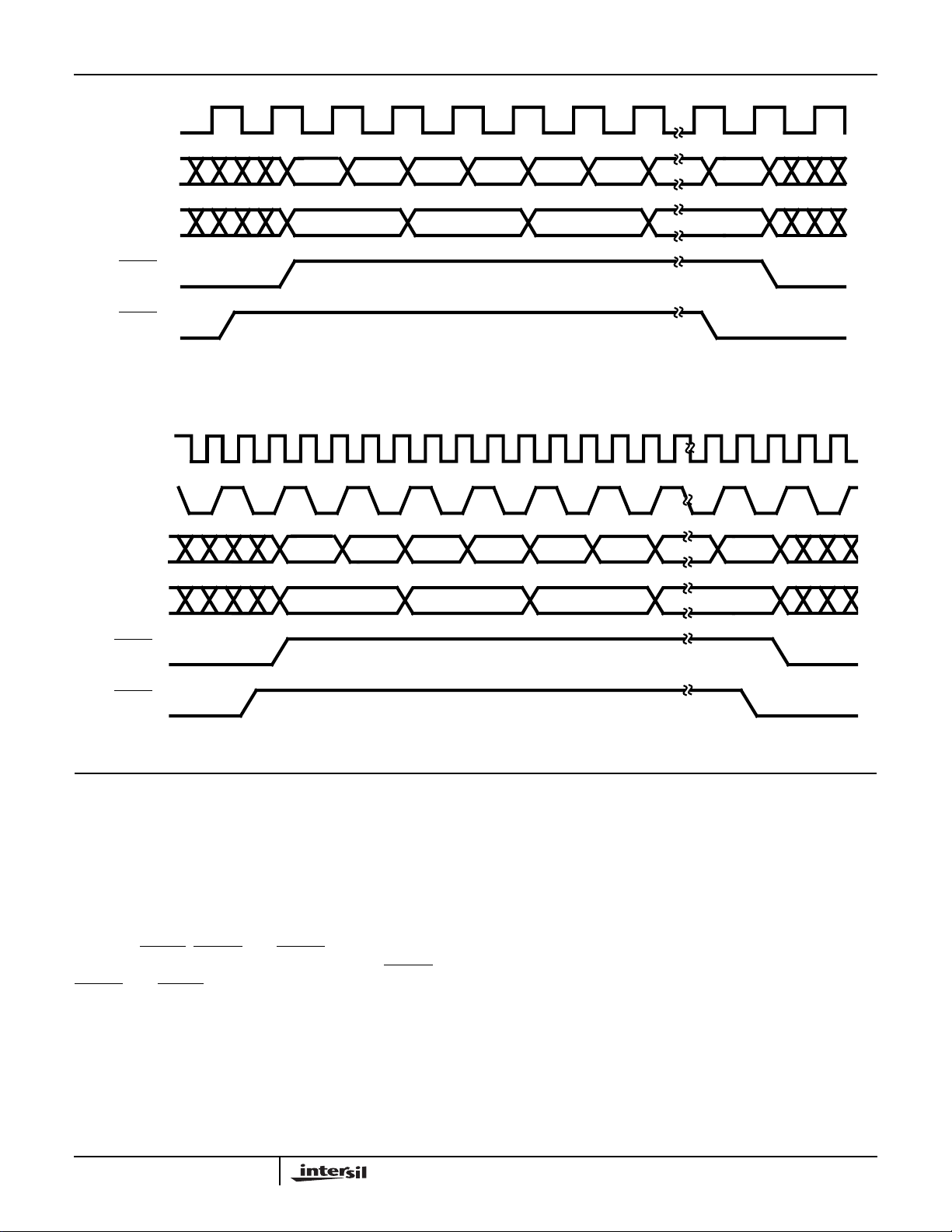
The pixel and overlay input timing is shown in Figure 1.
As inputs,
each rising edge of CLK2. As outputs,
VSYNC are output following the rising edge of CLK2. If the
CLK pin is configured as an input, it is ignored. If configured
as an output, it is one-half the CLK2 frequency.
BLANK, HSYNC, and VSYNC are latched on
BLANK, HSYNC, and
6
8-Bit YCbCr Format with 2X Upscaling
When 8-bit YCbCr format is selected and 2X upscaling is
enabled, the data is latched on the rising edge of CLK2 while
CLK is low. The pixel data must be [Cb Y Cr Y’ Cb Y Cr
Y’. . . ], with the first active data each scan line being Cb
data. Overlay data is latched on the rising edge of CLK2 that
latches Y pixel input data. The pixel and overlay input timing
is shown in Figure 2.
As inputs,
rising edge of CLK2 while CLK is low. As outputs,
VSYNC, and BLANK are output following the rising edge of
CLK2 while CLK is high. In this mode of operation, CLK is
one-half the CLK2 frequency.
BLANK, HSYNC, and VSYNC are latched on the
HSYNC,
CLK2
HMP8154, HMP8156A
P8-P15
OL0-OL2,
M1, M0
BLANK
(INPUT)
BLANK
(OUTPUT)
CLK2
CLK
OL0-OL2,
M1, M0
Cb 0 Y 0 Cr 0 Y 1 Cb 2 Y 2
PIXEL 0 PIXEL 1 PIXEL 2
FIGURE 1. PIXEL AND OVERLAY INPUT TIMING - NORMAL 8-BIT YCBCR
Cb 0 Y 0 Cr 0 Y 1 Cb 2 Y 2P8-P15
PIXEL 0 PIXEL 1 PIXEL 2
Y N
PIXEL N
Y N
PIXEL N
BLANK
(INPUT)
BLANK
(OUTPUT)
FIGURE 2. PIXEL AND OVERLAY INPUT TIMING - 8-BIT YCBCR WITH 2X UPSCALING
Normal 16-Bit YCbCr, 16-Bit RGB, 24-Bit RGB
Formats
When 16-bit YCbCr, 16-bit RGB data, or 24-bit RGB format
is selected without 2X upscaling or flicker filtering, the pixel
data is latched on the rising edge of CLK2 while CLK is low.
Overlaydatais also latched on the rising edge of CLK2 while
CLK is low. The pixel and overlay input timing is shown in
Figures 3 - 5.
As inputs,
rising edge of CLK2 while CLK is low. As outputs,
VSYNC, and BLANK are output following the rising edge of
CLK2 while CLK is high. In these modes of operation, CLK is
one-half the CLK2 frequency.
BLANK, HSYNC, and VSYNC are latched on the
HSYNC,
7
CLK2
CLK
HMP8154, HMP8156A
P8-P15
OL0-OL2,
M1, M0
BLANK
(INPUT)
BLANK
(OUTPUT)
CLK2
CLK
P0-P15
OL0-OL2,
M1, M0
Y 0Y 1Y 2Y 3Y 4Y 5
Cb 0 Cr 0 Cb 2 Cr 2 Cb 4 Cr 4P0-P7
PIXEL 0 PIXEL 1 PIXEL 2 PIXEL 3 PIXEL 4 PIXEL 5
FIGURE 3. PIXEL AND OVERLAY INPUT TIMING - NORMAL 16-BIT YCBCR
RGB 0 RGB 1 RGB 2 RGB 3 RGB 4 RGB 5
PIXEL 0 PIXEL 1 PIXEL 2 PIXEL 3 PIXEL 4 PIXEL 5
Y N
Cr N-1
PIXEL N
RGB N
PIXEL N
BLANK
(INPUT)
BLANK
(OUTPUT)
CLK2
CLK
P0-P24
BLANK
(INPUT)
BLANK
(OUTPUT)
FIGURE 4. PIXEL AND OVERLAY INPUT TIMING - NORMAL 16-BIT RGB
RGB 0 RGB 1 RGB 2 RGB 3 RGB 4 RGB 5
FIGURE 5. PIXEL AND OVERLAY INPUT TIMING - NORMAL 24-BIT RGB
8
RGB N
HMP8154, HMP8156A
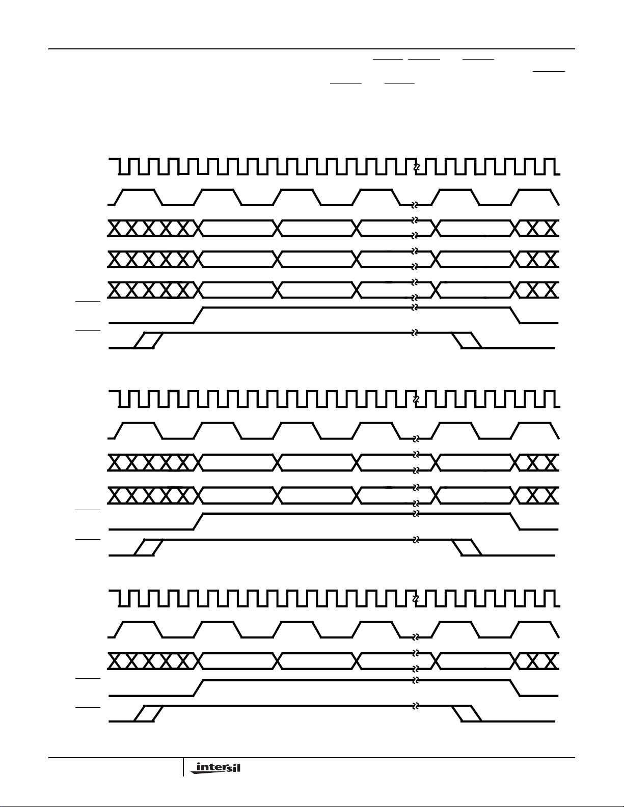
16-Bit YCbCr, 16-Bit RGB, 24-Bit RGB Formats
with 2X Upscaling
When 16-bit YCbCr, 16-bit RGB data, or 24-bit RGB format
is selected and 2X upscaling is enabled, data is latched on
the rising edge of CLK2 while CLK is low. Overlay data is
latched on the rising edge of CLK2 while CLK is low. The
pixel and overlay input timing is shown in Figures 6-8.
CLK2
CLK
P8-P15
P0-P7
OL0-OL2,
M1, M0
BLANK
(INPUT)
BLANK
(OUTPUT)
Y 0 Y 1 Y N
Cb 0 Cr 0 Cr N-1
PIXEL 0 PIXEL 1 PIXEL N
As inputs,
rising edge of CLK2 while CLK is low. As outputs,
BLANK, HSYNC, and VSYNC are latched on the
HSYNC,
VSYNC, and BLANK are output following the rising edge of
CLK2 while CLK is high. CLK is one-fourth the CLK2
frequency.
CLK2
CLK
P0-P15
OL0-OL2,
M1, M0
BLANK
(INPUT)
BLANK
(OUTPUT)
CLK2
CLK
P0-P24
FIGURE 6. PIXEL AND OVERLAY INPUT TIMING - 16-BIT YCBCR WITH 2X UPSAMPLING
RGB 0 RGB 1 RGB N
PIXEL 0 PIXEL 1 PIXEL N
FIGURE 7. PIXEL AND OVERLAY INPUT TIMING - 16-BIT RGB WITH 2X UPSAMPLING
RGB 0 RGB 1 RGB N
BLANK
(INPUT)
BLANK
(OUTPUT)
FIGURE 8. PIXEL AND OVERLAY INPUT TIMING - 24-BIT RGB WITH 2X UPSAMPLING
9
HMP8154, HMP8156A
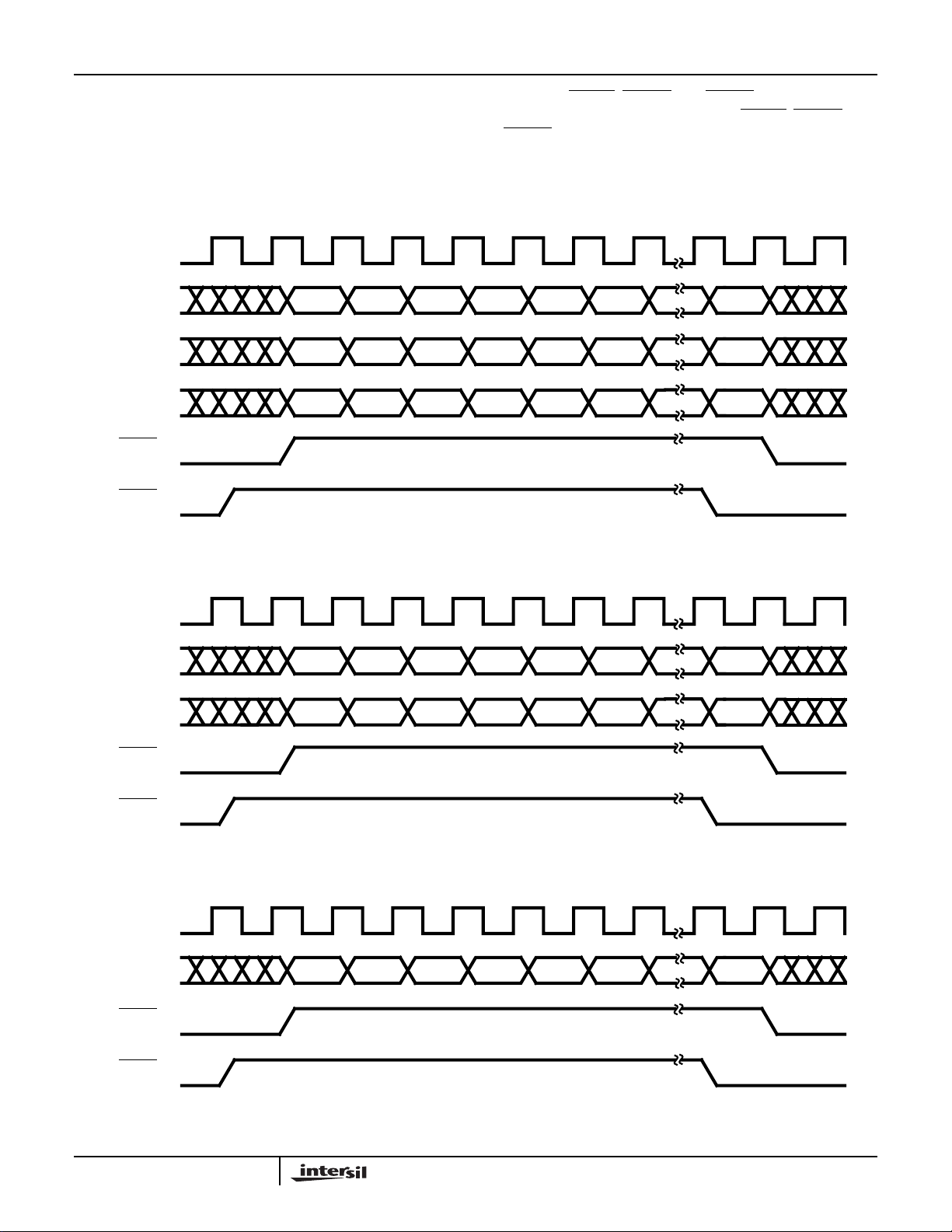
16-Bit YCbCr, 16-Bit RGB, 24-Bit RGB Formats
with Flicker Filtering
When the 16-bit YCbCr, 16-bit RGB, or 24-bit RGB data
format is selected and flicker filtering is enabled, pixel and
overlay data is latched on every rising edge of CLK2. The
pixel and overlay input timing is shown in Figures 9-11.
CLK2
Y 0 Y 1 Y 2 Y 3 Y 4 Y 5P8-P15
Cb 0 Cr 0 Cb 2 Cr 2 Cb 4 Cr 4P0-P7
OL0-OL2,
M1, M0
BLANK
(INPUT)
BLANK
(OUTPUT)
FIGURE 9. PIXEL AND OVERLAY INPUT TIMING - 16-BIT YCBCR WITH FLICKER FILTERING
PIXEL 0 PIXEL 1 PIXEL 2 PIXEL 3 PIXEL 4 PIXEL 5
As inputs,
each rising edge of CLK2. As outputs,
BLANK, HSYNC, and VSYNC are latched on
BLANK, HSYNC, and
VSYNC are output following the rising edge of CLK2. If the
CLK pin is configured as an input, it is ignored. If configured
as an output, it is one-half the CLK2 frequency.
Y N
Cr N-1
PIXEL N
CLK2
P0-P15
OL0-OL2,
M1, M0
BLANK
(INPUT)
BLANK
(OUTPUT)
CLK2
P0-P23
BLANK
(INPUT)
RGB 0 RGB 1 RGB 2 RGB 3 RGB 4 RGB 5 RGB N
PIXEL 0 PIXEL 1 PIXEL 2 PIXEL 3 PIXEL 4 PIXEL 5
PIXEL N
FIGURE 10. PIXEL AND OVERLAY INPUT TIMING - 16-BIT RGB WITH FLICKER FILTERING
RGB 0 RGB 1 RGB 2 RGB 3 RGB 4 RGB 5
RGB N
BLANK
(OUTPUT)
FIGURE 11. PIXEL AND OVERLAY INPUT TIMING - 24-BIT RGB WITH FLICKER FILTERING
10
CLK2
(
HMP8154, HMP8156A
P8-P15
OL0-OL2,
M1, M0
BLANK
OUTPUT)
Cb 2 Y 2 Cr 2 Y 3 Cb 4 Y 4
PIXEL 0 PIXEL 1
FIGURE 12. PIXEL AND OVERLAY INPUT TIMING - BT.656
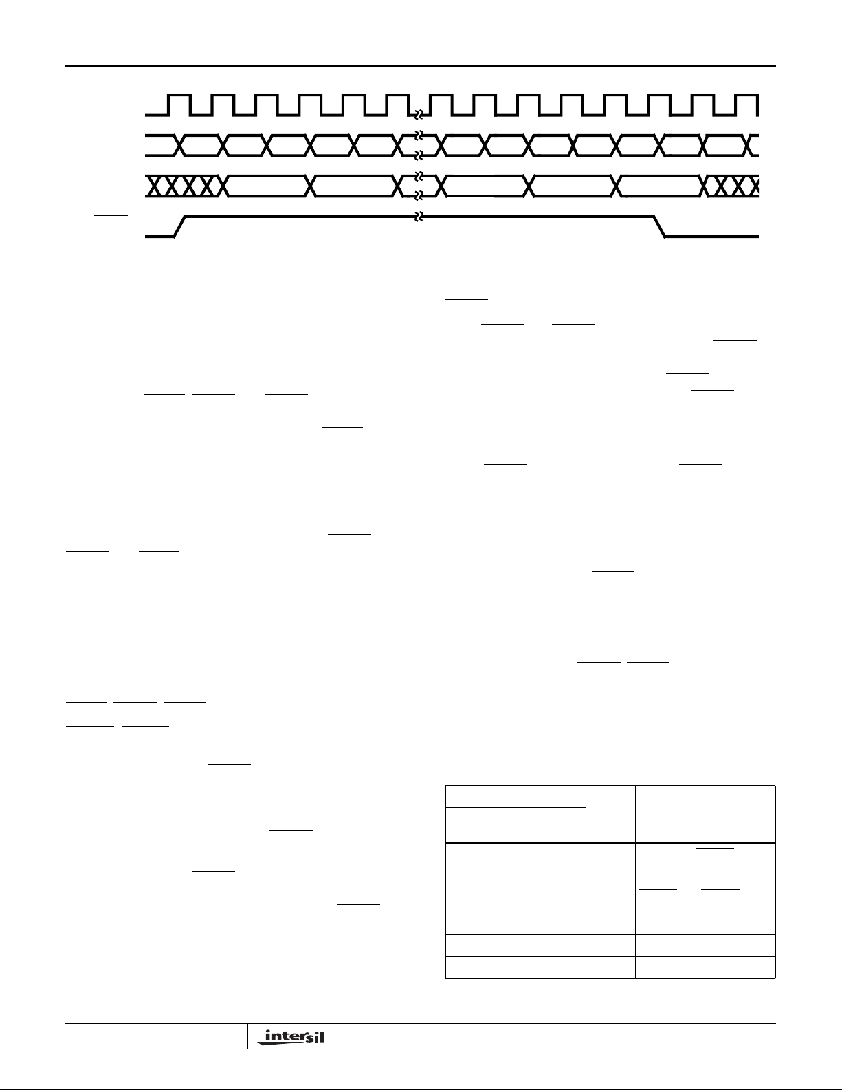
8-Bit BT.656 Format
When BT.656 format is selected, data is latched on each
rising edge of CLK2. Overlay data is latched when the Y
input data is latched. However, the overlay data must arrive
three pixels after its corresponding Y data. The pixel and
overlay input timing is shown in Figure 12.
As inputs, the
BLANK, HSYNC, and VSYNC pins are
ignored since all timing is derived from the EAV and SAV
sequences within the data stream. As outputs,
BLANK,
HSYNC and VSYNC are output following the rising edge of
CLK2. If the CLK pin is configured as an input, it is ignored. If
configured as an output, it is one-half the CLK2 frequency.
Square pixel operation, overlay processing with internal
mixing, flicker filtering, and SIF mode 2X upsampling are not
supported for the BT.656 input format. Also, the
HSYNC,
VSYNC, and BLANK signals must be configured as outputs.
Video Timing Control
Regardless of the input mode, the output video timing of the
HMP8154/HMP8156A is at 50 or 59.94 fields per second
(interlaced). For normal and 2X upscaling modes, the pixel
input timing is at 50 or 59.94 fields per second; with the
flickerfilterenabled,the input timing rate is twice as fast. The
output video and pixel input timing is controlled by the
BLANK, HSYNC, VSYNC, FIELD, and CLK2 pins.
HSYNC, VSYNC, and Field Timing
The leading edge of HSYNC indicates the beginning of a
horizontal sync interval. If
for about 4.7µs. If
HSYNC is an input, it must be active for at
least two CLK2 periods. The width of the horizontal
composite sync tip is determined from the video standard
and does not depend on the width of
The leading edge of VSYNC indicates the beginning of a
vertical sync interval.If
3 scan lines in (M, NSM) NTSC and (M, N) PAL modes or
2.5 scan lines in (B, D, G, H, I, CN) PAL modes. If
an input, it must be asserted for at least two CLK2 periods.
When
HSYNC and VSYNC are configured as outputs, their
leading edges will occur simultaneously at the start of an
HSYNC is an output, it is asserted
HSYNC.
VSYNC is an output, it is asserted for
VSYNC is
"FF" "00"
PIXEL N-2 PIXEL N-1
"00" "XY" "10"
"10""80"
PIXEL N
odd field. At the start of an even field, the leading edge of
VSYNC occurs in the middle of the line.
When HSYNC and VSYNC are configured as inputs, the
HMP8154/HMP8156A provides a programmable
HSYNC
window for determining FIELD. The window is specified with
respect to the leading or trailing edge of
is selected in the field control register. When
VSYNC. The edge
HSYNC is
found inside the window,then the encoder sets FIELD to the
value specified in the field control register.
The HMP8154/HMP8156A provides programmable timing
for the
VSYNC input. At the active edge of VSYNC, the
encoder resets its vertical half-line counter to the value
specified by the field control register. This allows the input
and output syncs to be offset, although the data must still be
aligned.
The FIELD signal is always an output and changes state
near each leading edge of
VSYNC. The delay between the
syncs and FIELD depends on the encoder’soperating mode
as summarized in Table 6. In modes in which the encoder
uses CLK to gate its inputs and outputs, the FIELD signal
may be delayed 0-12 additional CLK2 periods.
Figure 13 illustrates the
HSYNC, VSYNC, and FIELD
general timing for (M, NSM) NTSC and (M, N) PAL. Figure
14 illustrates the general timing for (B, D,G,H, I, CN) PAL.In
the figures, all the signals are shown active low (their reset
state), and FIELD is low during odd fields.
TABLE 6. FIELD OUTPUT TIMING
OPERATING MODE
SYNC I/O
DIRECTION
Input Input 148 FIELD lags VSYNC switch-
Input Output 138 FIELD lags VSYNC.
Output Don’t Care 32 FIELD leadsVSYNC.
BLANK I/O
DIRECTION
CLK2
DELAY COMMENTS
ing from odd to even.
FIELD lags the earlier of
VSYNC and HSYNC when
syncs are aligned when
switching from even toodd.
11
 Loading...