

Intersil Corporation HMP8117 Datasheet

HMP8117
Data Sheet January 1999 File Number
NTSC/PAL Video Decoder
The HMP8117 is a high quality NTSC and PAL video
decoder with internal A/D converters. It is compatible with
NTSC M, PAL B, D, G, H, I, M, N, and combination N (N
video standards.
Both composite and S-video (Y/C) input formats are
supported. A 2-line comb filter plus a user-selectable
chrominance trap filter provide high quality Y/C separation.
User adjustments include brightness, contrast, saturation,
hue, and sharpness.
Vertical blanking interval (VBI) data, such as Closed
Captioning, Wide Screen Signalling and Teletext, may be
captured and output as BT.656 ancillary data. Closed
Captioning and Wide Screen Signalling information mayalso
be read out via the I
The Videolyzer™ feature provides approved Macrovision
copy-protection bypass and detection.
2
C interface.
)
C
™
Ordering Information
TEMP RANGE
PART NUMBER
HMP8117CN 0 to 70 80 Ld PQFP Q80.14x20
HMPVIDEVAL/ISA Evaluation Board: ISA Frame Grabber
NOTES:
1. PQFP is also known as QFP and MQFP.
2. Evaluation Board descriptions are in the Applications section.
(oC) PACKAGE
PACKAGE
NO.
4643
Features
• (M) NTSC and (B, D, G, H, I, M, N, NC) PAL Operation
- Optional Auto Detect of Video Standard
- ITU-R BT.601 (CCIR601) and Square Pixel Operation
• Videolyzer Feature
- Macrovision™ Bypass and Detection
• Digital Anti-Alias Filter
• Power Down Mode
• Digital Output Formats
- VMI Compatible
- 8-bit, 16-bit 4:2:2 YCbCr
- 15-bit (5,5,5), 16-bit (5,6,5) RGB
- Linear or Gamma-Corrected
- 8-bit BT.656
• Analog Input Formats
- Three Analog Composite Inputs
- Analog Y/C (S-video) Input
• “Raw” (Oversampled) VBI Data Capture
• “Sliced” VBI Data Capture Capabilities
- Closed Captioning
- Widescreen Signalling (WSS)
- BT.653 System B, C and D Teletext
- North American Broadcast Teletext (NABTS)
- World System Teletext (WST)
• 2-Line (1H) Comb Filter Y/C Separator
2
• Fast I
C Interface
Applications
• Multimedia PCs
• Video Conferencing
• Video Compression Systems
• Video Security Systems
• LCD Projectors and Overhead Panels
• Related Products
- NTSC/PAL Encoders: HMP815x, HMP817x, HMP819x
- NTSC/PAL Decoders: HMP8112A, HMP8115
1
CAUTION: These devices are sensitive to electrostatic discharge; follow proper IC Handling Procedures.
Videolyzer™ is a trademark of Intersil Corporation. Macrovision™ is a trademark of Macrovision Corporation.
http://www.intersil.com or 407-727-9207 | Copyright © Intersil Corporation 1999
P[15:0]
HSYNC
VSYNC
OUTPUT
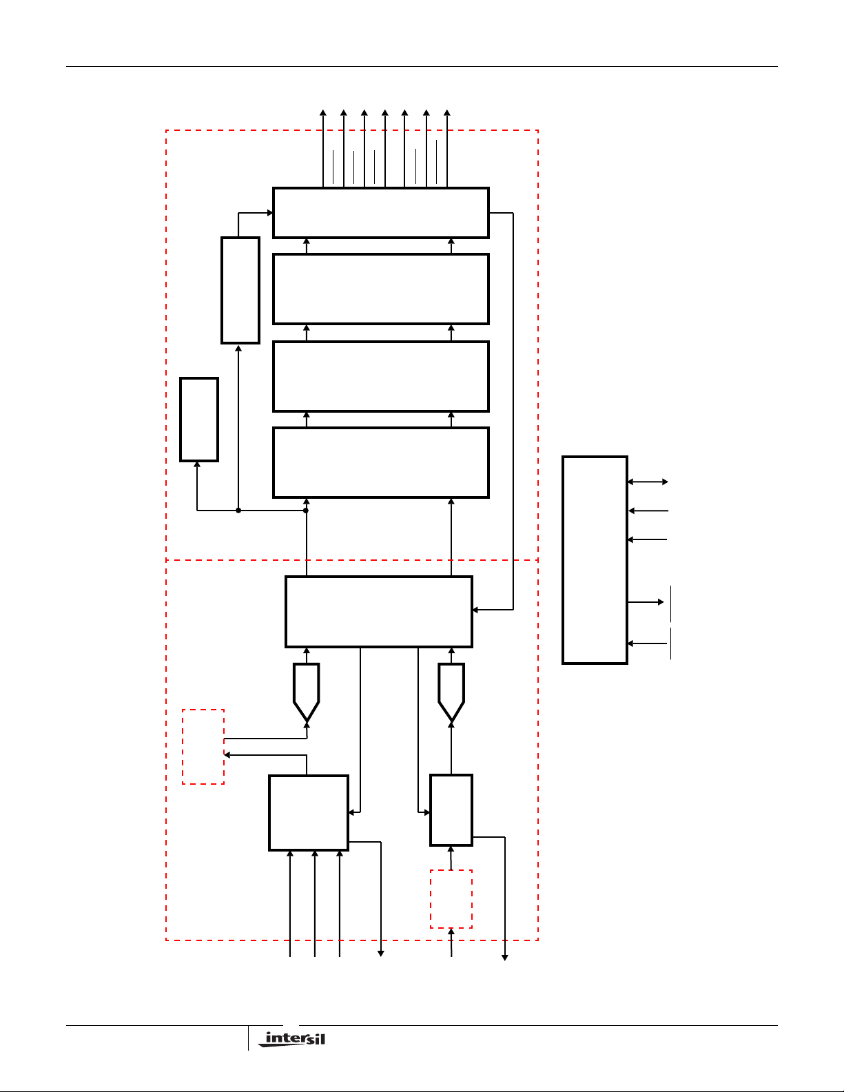
HMP8117
FIELD
DVALID
BLANK
FIFO
AND
DAT A
TIMING
VBIVALID
SEE DIGITAL PROCESSING BLOCK DIAGRAM
DETECT
MACROVISION
VBI
DETECTION &
DECODING LOGIC
YIN[7:0]
ADC
OUTPUT
SAMPLE
Y/C
AND
SEPARATION
INPUT
SAMPLE
CONTROL
FINE AGC,
DC-RESTORE
RATE
CONVERTER
USER
RATE
CONVERTER
ADJUSTS
CIN[7:0]
ADC
SYNC-TIP, BACKPORCH TIMING
INTERFACE AND
MICROPROCESSOR
CONTROL
INTREQ SA SCLSCL
RESET
Functional Block Diagram
SEE ANALOG FRONT END BLOCK DIAGRAM
FILTER
EXTERNAL
ANTI-ALIAS
2
IN
Y
OUT
Y
CVBS1
COMPOSITE/LUMA
INPUT CLAMP,
MUX,
COARSE AGC,
CVBS2
DC-RESTORE
CVBS3(Y)
LCAP
DC-RESTORE
COARSE AGC
C
EXTERNAL
ANTI-ALIAS
CHROMA
CCAP
FILTER

Analog Front End Block Diagram
(INTERNAL CLAMP)(EXTERNAL)
VAA
INPUT
VIDEO
3
VID1
VID2
Y_IN
75
75 75
STORAGE
CHROMA INPUT
1.0µF
C_IN
75
STORAGE
PIN #
7
65
9
8
19
17
1.0µF
75
1.0µF
1.0µF
1.0µF
CAP
EXTERNAL
ANTI-ALIAS
FILTER
CAP
NOMINAL (NTSC) OPERATING CONDITION
CVBSX. SIZE = INPUT. SYNC TIP CLAMPED AT ~= 1.75 VDC.
Y
OUT/YIN
C. SIZE = INPUT SIZE. PORCH OFFSET ~= 2.0 VDC.
A/D_TEST. SIZE ~= F(LUMA AGC), PORCH OFFSET ~= 2.0VDC.
nmos
#
PIN
CVBS1
CVBS2
CVBS3(Y)
LCAP
76
0.1µF
C
19
CCAP
0.1µF
. SIZE = ~1.0 V
7
6
5
29
#
1.75V
+
-
50µA
(SIGNAL BIAS ~ 2.0V)
(OFFSET CHROMA SIGNAL TO ADC MID-SCALE ~= 2.0V)
DECODER PIN #
TO
MUX
CHROMA
ATTEN
(BELOW)
CLAMP
CLAMP
CLAMP
1.75V
REF
(OFFSET LUMA SIGNAL TO LOWER ADC REF ~= 1.5V)
M
U
X
MUX
SELECT
ATTENUATOR
ATTENUATOR
13
13-STEP
VARIABLE
1.75V
CHROMA
ATTEN
13-STEP
VARIABLE
2.0V
4 TO 13
DECODER
2X
2X
PIN #
76
, SYNC TIP OFFSET ~= 1.5 VDC.
P-P
29
28
78
GAIN CONTROL
SET POINT
CHROMA MULT.
(BELOW)
Y
OUT
EXTERNAL
9
ANTI-ALIAS
FILTER
CHARGE PUMP
100µA
100µA
A/D_TEST
CHARGE PUMP
100µA
100µA
4
11
Y
17
GAIN
CORRECTION
LOGIC
FINE ADJUST MULT. FACTOR
2.5V
IN
8
BUF
DISCHARGE
CHARGE
SYNC-TIP ENABLE
BUF
DISCHARGE
CHARGE
SYNC-TIP ENABLE
10-BIT
ADC
1.5V
LUMA
DC-RESTORE
LOGIC
2.5V
10-BIT
ADC
1.5V
CHROMA
DC-RESTORE
LOGIC
NOMINAL (NTSC) OPERATING CONDITION
LCAP. DC-SIGNAL OFFSET ~= 2.4 VDC.
CCAP. DC-SIGNAL OFFSET ~= 2.4 VDC.
RSET. DC-SIGNAL OFFSET ~= 1.2 VDC.
REF_CAP. DC-SIGNAL OFFSET ~= 2.5 VDC.
BACKPORCH
ENABLE
LOW-PASS
FILTER
(REMOVE Fsc)
DIGITAL
10
ANTI-
ALIAS
FILTER
DISABLE
DIGITAL
10
ANTI-
ALIAS
FILTER
DISABLE
REFERENCE
CHROMA
BIAS/
INTERNAL
CORRECTION
MULTIPLIER
MULT.
CORRECTION
MULTIPLIER
28
78
TRUNCATE
8-BIT
Y[7:0]
TRUNCATE
8-BIT
C[7:0]
POWERDOWN
RSET
REF_CAP
1.0µF
HMP8117
12.1K

LOCK
STATUS
FILTER
PLL LOOP
LINE LOCKED
NCO
LINE LOCKED
HMP8117
HSYNC
P[15:0]
VSYNC
OUTPUT
SYNC
STRIPPER,
CbCr
FIELD
BLANK
FIFO
DAT A
AND
TIMING
DAT A
TIMING
AND
RGB
ADJUST,
CONTRAST
BRIGHTNESS
RATE
OUTPUT
SAMPLE
CONVERTER
DVALID
VBIVALID
CONVERSION
Y
SELECT
STANDARD
PHASE
CHROMA
DETECTOR
HUE
ADJUST
FILTER
CHROMA
PLL LOOP
PLL NCO
CHROMA
CLK2 FREQ SELECT
(24.54, 27.0 or 29.5MHz)
TO FIFO
VSYNC
FIELD AND
VSYNC
DETECT
CHROMA
AGC AND
CLK2 TO
4FSC RATIO
4FSC
ADJUST
SATURATION
CHROMA DATA
CLOCK
LP FILTER
CHROMA
U/V TO CbCr
COLOR SPACE
U, V
CHROMA
LINE
M
DELAY
C, CVBS
U
ENABLE
CONVERTER,
COLOR KILLER
DEMOD
COMB
FILTER
INPUT
SAMPLE
X
RATE
TRAP
CHROMA
CONVERTER
M
NORMAL
HORIZONTAL
AND VERTICAL
M
U
U
Y LUMA DATA
X
LP FILTER
ADJUST
SHARPNESS
X
FILTER
SELECT
ADJUST
SHARPNESS
VBI DETECTION
VBI STATUS
MV STATUS
DETECT
MACROVISION
AND DECODING LOGIC
Digital Processing Block Diagram
C[7:0]
Y[7:0]
4

HMP8117
Introduction
The HMP8117 is designed to decode baseband composite
or S-video NTSC and PAL signals, and convert them to
either digital YCbCr or RGB data. In addition to performing
the basic decoding operations, these devices include
hardware to decode different types of VBI data and to
generate full-screen blue, black and color bar patterns.
Digital PLLs are used to synchronize to all NTSC and PAL
standards. A chroma PLL is used to maintain color lock for
chroma demodulation while a line-locked PLL is used to
maintain vertical spatial alignment. The PLLs are designed
to maintain lock in the presence of VCR head switches, VCR
trick-mode and multi-path noise.
The HMP8117 provides the Videolyzer feature for
Macrovision (MV) copy-protection bypass and detection.
External Video Processing
Before a video signal can be digitized the decoder has some
external processing considerations that need to be
addressed. This section discusses those external aspects of
the HMP8117.
Analog Video Inputs
The HMP8117 supports either three composite or two
composite and one S-video input.
Three analog video inputs (CVBS 1-3) are used to select
which one of three composite video sources are to be
decoded. To support S-video applications, the Y channel
drives the CVBS3(Y) analog input, and the C channel drives
the C analog input.
The analog inputs must be AC-coupled to the video signals,
as shown in the Applications section.
Digitization of Video
Prior to A/D conversion, the input signal is offset and scaled to
known video levels. After digitization, sample rate converters
and a comb filter are used to perform color separation and
demodulation.
A/D Conversion
Each CVBSX video input channel has a video clamp circuit
that is independent of PLL timing. The input clamp provides
a coarse signal offset to position the sync tip within the A/D
converter sampling range so that the AGC and DCRESTORE logic can operate.
A/D Conversion
Video data is sampled at the CLK2 frequency then processed
by the input sample rate conv erter. The output levels of the
ADC after AGC and DC restoration processing are:
(M) NTSC
(M, N) PAL
white 196 196
black 66 59
blank 56 59
sync 0 0
AGC and DC Restoration
The AGC amplifier attenuates or amplifies the analog video
signal to ensure that the blank lev el gener ates code 56 or 59
depending on the video standard. The difference from the
ideal blank lev el of 56 or 59 is used to control the amount of
attenuation or gain of the analog video signal. To obtain a
stable DC reference f or the AGC, a digital low-pass filter
removes the chroma burst from the input signal’s backporch.
(B, D, G, H, I, NC)
PAL
Anti-alias Filters
Although a 23 tap digital halfband anti-alias filter is provided
for each A/D channel, an external passive filter is
recommended for optimum performance. The digital filter
has a flat response out to 5.4MHz with an approximate -3dB
bandwidth of 6.3MHz using a 27MHz input CLK2 sample
rate. For the CVBSx inputs, the filter is connected between
the YOUT and YIN pins. For the C (chroma) input, the antialias filter should be connected before the C input.
Recommended filter configurations are shown on the
reference schematic in Figure 20. These filters have flat
response out to 4.2MHz with an approximate -3dB
bandwidth of 8MHz. If upgrading from the HMP8115 or
HMP8112A, the previous filter configurations may be used
but with slightly degraded bandwidth. Alternative higher or
lower performance filters configurations may substituted.
5
DC restoration positions the video signal so that the sync tip
generates a code 0. The internal timing windows for AGC
and DC restoration are show in Figure 3. The appropriate
windows are automatically determined by the decoder when
the input signal is auto-detected or manually selected.
VIDEO INPUT
AGC
DC RESTORE
FIGURE 1. AGC AND DC RESTORE INTERNAL TIMING

HMP8117
Input Signal Detection
If no input video signal is detected for 16 consecutive line
periods, nominal video timing is generated for the previously
detected or programmed video standard. A maskable
interrupt is provided for the condition of “Input Signal Loss”
allowing the host to enable blue field output if desired.
Vertical Sync and Field Detection
The vertical sync and field detect circuit uses a low time
counter to detect the vertical sync sequence in the video
data stream. The low time counter accumulates the low time
encountered during any sync pulse, including serration and
equalization pulses. When the low time count exceeds the
vertical sync detect threshold,
VSYNC is asserted
immediately. FIELD is asserted at the same time that
VSYNC is asserted. FIELD is asserted low forodd fields and
high for even fields. Field is determined from the location in
the video line where VSYNC is detected. If VSYNC is
detected in the first half of the line, the field is odd. If VSYNC
is detected in the second half of a line, the field is even.
In the case of lost vertical sync or excessive noise that would
prevent the detection of v ertical sync, the FIELD output will
continue to toggle. Lost vertical sync is declared if after 337
lines, a vertical sync period was not detected for 1 or 3
(selectable) successive fields as specified by bit 2 of the
GENLOCK CONTROL register 04
. When this occurs, the
H
PLLs are initialized to the acquisition state.
Y/C Separation
A composite video signal has the luma (Y) and chroma (C)
information mixed in the same video signal. The Y/C
separation process is responsible for separating the
composite video signal into these two components. The
HMP8117 utilizes a comb filter to minimize the artifacts that
are associated with the Y/C separation process.
Input Sample Rate Converter
The input sample rate converter is used to convert video data
sampled at the CLK2 rate to a virtual 4xf
comb filtering and color demodulation. An interpolating filter is
used to generate the 4xf
samples as illustrated in Figure 2.
SC
sample rate for
SC
Comb Filter
A 2-line comb filter, using a single line delay, is used to
perform part of the Y/C separation process. During S-video
operation, the Y signal bypasses the comb filter; the C signal
is processed by the comb filter since it is an integral part of
the chroma demodulator. During PAL operation, the chroma
trap filter should also be enabled for improved performance.
Since a single line store is used, the chroma will normally
have a half-line vertical offset from the luma data. This may
be eliminated, vertically aligning the chroma and luma
samples, at the expenseofvertical resolution of the luma. Bit
0 of the OUTPUT FORMAT register 02
controls this option.
H
Chroma Demodulation
The output of the comb filter is further processed using a
patented frequency domain transform to complete the Y/C
separation and demodulate the chrominance.
Demodulation is done at a virtual 4xf
sample rate using
SC
the interpolated data samples to generate U and V data. The
demodulation process decimates by 2 the U/V sample rate.
Output Sample Rate Converter
The output sample rate converter converts the Y, U and V data
from a virtual 4xf
sample rate to the desired output sample
SC
rate (i.e., 13.5MHz). It also vertically aligns the samples based
on the horizontal sync information embedded in the digital
video data stream.Theoutputsamplerateisdeterminedbythe
input video standard and the selected rectangular/square pixel
mode. The output pixel rate is 1/2 of the CLK2 input clock
frequency. The output format is 4:2:2 for all modes except the
RGB modes which use a 4:4:4 output format.
CLK2 Input
The decoder requires a stable clock source for the CLK2
input. For best performance, use termination resistor(s) to
minimize pulse overshoot and reflections on the CLK2 input.
Since chroma demodulation uses the virtual 4xf
on CLK2 will be transferred as chrominance error on the
output pixels. The CLK2 clock frequency must be one of the
valid selections from Table 1 below based on the video
standard and desired pixel mode.
, any jitter
SC
INCOMING VIDEO SAMPLES
TIME
RESAMPLED VIDEO
TIME
4xf
SC
FIGURE 2. SAMPLE RATE CONVERSION
6
TABLE 1. VIDEO STANDARDCLOCKRATE SELECTION
SUMMARY
VALID CLK2
FREQUENCIES (MHz)
RECTANGULAR
VIDEO FORMAT
(M) NTSC, (M) PAL 27.00 24.54
(B, D, G, H, I,N,NC) PAL 27.00 29.50
PIXEL MODE
SQUARE PIX-
EL MODE
The CLK2 should be derived from a stable clock source,
such as a crystal. CLK2 must have at least a ±50ppm
accuracy and at least a 60/40% duty cycle to ensure proper

HMP8117
operation. Use of a PLL to generate a “Line Locked” CLK2
input based on the input video is not recommend. (See next
section below.)
Cycle Slipping and Real-Time Pixel Jitter
The decoder’s digital PLL allows it to maintain lock and
provide high quality Y/C separation even on the poorest
quality input video signals. However, this architecture does
not provide a “Line Lock Clock” output and should
used as a timing master for direct interface to another video
encoder in a system.
Since the decoder uses a fixed CLK2 input frequency, the
output pixel rate must be periodically adjusted to
compensate for any frequency error between CLK2 and the
input video signal. This output pixel rate adjustment is
referred to as cycle slipping. Since the decoder has an
output data FIFO, all cycle slipping can be deferred until the
next horizontal blanking interval. This guarantees a
consistent number of pixels during the active video region.
Due to cycle slipping, the output timing and data will exhibit a
nominal real-time (line-to-line) pixeljitterofoneCLK2period.
Although the sample rate converter maintains a 1/8 pixel
vertical sample alignment, the output data must be routed to
a frame buffer or video compression chip in order remove
the effects of cycle slipping. (The frame buffer or
compression chip serves as a time base corrector.)
By directly interfacing the decoder to a video encoder, the
output video signal will directly reflect the real-time pixel jitter
effects of the decoder output timing. The jitter effects can be
visualized on a CRT monitor using a static image containing
patterns with sharp vertical edges. The edges will appear
more “ragged” when compared to the input video signal. The
severity of this visual effect relates directly to the frequency
error between CLK2 and the input video signal. It is nearly
impossible to completely match CLK2 with the input video
signal. Therefore, a direct decoder to encoder interface is
not recommended.
The use of an external PLL to generate a “Line Locked”
CLK2 input derived from the input video signal is also not
recommended, since this will defeat the internal digital PLL
and result in pixel decoding errors.
not be
Digital Processing of Video
Once the luma and chroma have been separated the
HMP8117 then performs programmable modifications (i.e.
contrast, coring, color space conversions,color AGC,etc.)to
the decoded video signal.
UV to CbCr Conversion
The baseband U and V signals are scaled and offset to
generate a nominal range of 16-240 for both the Cb and Cr
data.
Digital Color Gain Control
There are four types of color gain control modes available:
no gain control, automatic gain control, fixed gain control,
and freeze automatic gain control.
If “no gain control” is selected, the amplitude of the color
difference signals (CbCr) is not modified, regardless of
variations in the color burst amplitude. Thus, a gain of 1x is
always used for Cb and Cr.
If “automatic gain control” is selected, the amplitude of the
color difference signals (CbCr) is compensated for variations
in the color burst amplitude. The burst amplitude is averaged
with the two previous lines having a color burst to limit lineto-line variations. A gain of 0.5x to 4x is used for Cb and Cr.
If “fixed gain control” is selected, the amplitude of the color
difference signals (CbCr) is multiplied by a constant,
regardless of variations in the color burst amplitude. The
constant gain value is specified by the COLOR GAIN
register 1C
Limiting the gain to 4x limits the amount of amplified noise.
If “freeze automatic gain control” is selected, the amplitude of
the color difference signals (CbCr) is multiplied by a constant.
This constant is the value the AGC circuitry generated when
the “freeze automatic gain” command was selected.
. A gain of 0.5x to 4x is used for Cb and Cr.
H
Color Killer
If “enable color killer” is selected, the color output is turned
off when the running average of the color burst amplitude is
below approximately 25% of nominal for four consecutive
fields. When the running average of the color burst
amplitude is above approximately 25% of nominal for four
consecutive fields, the color output is turned on. The color
output is also turned off when excessive phase error of the
chroma PLL is present.
If “force color off” is selected, color information is never
present on the outputs.
If “force color on” is selected, color information is present on
the outputs regardless of the color burst amplitude or
chroma PLL phase error.
Y Processing
The black level is subtracted from the luminance data to
remove sync and any blanking pedestal information.
Negative values of Y are supported at this point to allow
proper decoding of “below black” luminance levels.
Scaling is done to position black at 8-bit code 0 and white at
8-bit code 219.
A chroma trap filter may be used to remov e any residual color
subcarrier from the luminance data. The center frequency of
the chroma trap is automatically determined from the video
standard being decoded. The chroma trap should be disabled
during S-video operation to maintain maximum luminance
bandwidth. Alternately, a 3MHz lo w-pass filter may be used to
7

HMP8117
remove high-frequency Y data. This may mak e a noisy image
more pleasing to the user, although softer.
Coring of the high-frequency Y data may be done to reduce
low-level high frequency noise.
Coring of the Y data may also be done to reduce low-level
noise around black. This forces Y data with the following
values to a value of 0:
coring = 1: ± 1
coring = 2: ± 1, ± 2
coring = 3: ± 1, ± 2. ± 3
High-frequency components of the luminance signal may be
“peaked” to control the sharpness of the image. Maximum
gain may be selected to occur at either 2.6MHz or the color
subcarrier frequency. This may be used to make the
displayed image more pleasing to the user. It should not be
used if the output video will be compressed, as the circuit
introduces high-frequency components that will reduce the
compression ratio.
The brightness control adds or subtracts a user-specified
DC offset to the Y data. The contrast control multiplies the Y
data by a user-specified amount. These may be used to
make the displayed image more pleasing to the user.
Finally, a value of 16 is added to generate a nominal range of
16 (black) to 235 (white).
CbCr Processing
The CbCr data is low-pass filtered to either 0.85MHz or
1.5MHz.
Coring of the CbCr data may be done to reduce low-level
noise around zero. This forces CbCr data with the following
values to a value of 128.
coring = 1: 127, 129
coring = 2: 126, 127, 129, 130
coring = 3: 125, 126, 127, 129, 130, 131
The saturation control multiplies the CbCr data by a userspecified amount. This may be used to make the displayed
image more pleasing to the user. The CbCr data may also
be optionally multiplied by the contrast value to avoid color
shifts when changing contrast.
The hue control provides a user-specified phase offset to the
color subcarrier during decoding. This may be used to
correct slight hue errors due to transmission.
YCbCr Output Format Processing
Y has a nominal range of 16 to 235. Cb and Cr have a
nominal range of 16 to 240, with 128 corresponding to zero.
Values less than 1 are made 1 and values greater than 254
are made 254.
While
BLANK is asserted, Y is forced to have a value of 16,
with Cb and Cr forced to have a value of 128, unless VBI
data is present.
RGB Output Format Processing
The 4:2:2 YCbCr data is converted to 4:4:4 YCbCr data and
then converted to either 15-bit or 16-bit gamma-corrected
RGB (R′G′B′) data. While
forced to a value of 0.
15-Bit R′G′B
The following YCbCr to R′G′B′ equations are used to
maintain the proper black and white levels:
R′ = 0.142(Y - 16) + 0.194(Cr - 128)
G′ = 0.142(Y - 16) - 0.099(Cr - 128) - 0.048(Cb - 128)
B′ = 0.142(Y - 16) + 0.245(Cb - 128)
The resulting 15-bit R′G′B′ data has a range of 0 to 31.
Values less than 0 are made 0 and values greater than 31
are made 31.
The 15-bit R′G′B′ data may be converted to 15-bit linear
RGB, using the following equations. Although the PAL
specifications specify a gamma of 2.8, a gamma of 2.2 is
normally used. The HMP8117 allows the selection of the
gamma to be either 2.2 or 2.8, independent of the video
standard.
for gamma = 2.2:
for R′G′B′ < 0.0812*31
for R′G′B′ >= 0.0812*31
for gamma = 2.8:
R = (31)(R′/31)
G = (31)(G′/31)
B = (31)(B′/31)
16-Bit R′G′B
The following YCbCr to R′G′B′ equations are used to
maintain the proper black and white levels:
R′ = 0.142(Y - 16) + 0.194(Cr - 128)
G′ = 0.288(Y - 16) - 0.201(Cr - 128) - 0.097(Cb - 128)
B′ = 0.142(Y - 16) + 0.245(Cb - 128)
The resulting 16-bit R′G′B′ data has a range of 0 to 31 for R′
and B′, and a range of 0 to 63 for G′. Values less than 0 are
made 0; R′ and B′ values greater than 31 are made 31, G′
values greater than 63 are made 63.
The 16-bit R′G′B′datamaybeconverted to 16-bit linear RGB,
using the followingequations.Although the PAL specifications
specify a gamma of 2.8, a gamma of 2.2 is normally used.
The HMP8117 allows the selection of the gamma to be either
2.2 or 2.8, independent of the video standard.
′
R = (31)((R′/31)/4.5)
G = (31)((G′/31)/4.5)
B = (31)((B′/31)/4.5)
R = (31)(((R′/31) + 0.099)/1.099)
G = (31)(((G′/31) + 0.099)/1.099)
B = (31)(((B′/31) + 0.099)/1.099)
′
BLANK is asserted, RGB data is
2.2
2.2
2.2
2.8
2.8
2.8
8

HMP8117
for gamma = 2.2:
for R′B′ < 0.0812*31, G′ < 0.0812*63
R = (31)((R′/31)/4.5)
G = (63)((G′/63)/4.5)
B = (31)((B′/31)/4.5)
for R′B′ >= 0.0812*31, G′ >= 0.0812*63
R = (31)(((R′/31) + 0.099)/1.099)
G = (63)(((G′/63) + 0.099)/1.099)
B = (31)(((B′/31) + 0.099)/1.099)
2.2
2.2
2.2
for gamma = 2.8:
R = (31)(R′/31)
G = (63)(G′/63)
B = (31)(B′/31)
2.8
2.8
2.8
Built-in Video Generation
The decoder can be configured to output a full-screen of built-in
blue, black or 75% color bar patterns. The type of pattern
generated is determined by bits 2-1 of the OUTPUT FORMAT
register 02
bits need to be set for normal operation to pass decoded video.
If the decoder is currently locked to a video source on the
input, the output data timing will be based on the input video
source. If an input video source is not detected, internallygenerated output data timing will be used. The following
table lists the data codes output for each built-in video
pattern in YCbCr format.
. When built-in video generation is not desired, the
H
Pixel Port Timing
The the timing and format of the output data and control
signals is presented in the following sections. Refer to the
section “CYCLE SLIPPING AND REAL-TIME PIXEL
JITTER” for PLL and interface considerations.
HSYNC and VSYNC Timing
The HSYNC and VSYNC output timing is VMI v1.4 compatible.
Figures 3-6 illustrate the video timing. The leading edge of
HSYNC is synchronous to the video input signal and has a
fixed latency due to internal pipeline processing. The pulse
width of the
36
, where the trailing edge of HSYNC has a programmable
H
delay of 0-510 CLK2 cycles from the leading edge.
Theleadingedgeof
through the first serration pulse of each field. An accumulator is
used to detect a low-time period within the serration pulse.
Since the leading edge of
used for timing with respect to
The trailing edge of VSYNC implements the VMI handshake
with
using the FIELD pin. For an odd field, the trailing edge of
VSYNC is 5 ±1 CLK2 cycles after the trailing edge of the
HSYNC that follows the last equalization pulse. Refer to
Figures 3 and 5. For an even field, the trailing edge of
is 5
±1 CLK2 cycles after the leading edge of the HSYNC that
follows the last equalization pulse. Refer to Figures 4 and 6.
HSYNC is defined by the END HSYNC register
VSYNCisasserted approximatelyhalfw a y
VSYNC is detected, it should not be
HSYNC or BLANK.
HSYNC in order to determine field information without
VSYNC
TABLE 2. BUILT-IN VIDEO PATTERN DATA CODES
PATTERN: COLOR Y Cb Cr
75% Color Bar: White
Magenta
Blue Screen: Blue 4B
Black Screen: Black 10
NTSC(M) LINE#
PAL(M) LINE#
VIDEO
INPUT
HSYNC
VSYNC
FIELD
Yellow
Cyan
Green
Red
Blue
Black
B4
A2
83
70
54
41
23
10
H
H
H
H
H
H
H
H
H
H
80
H
2C
H
9C
H
48
H
B8
H
64
H
D4
H
80
H
D9
H
80
H
12345678910525524
523
‘EVEN’ FIELD
5245251234567522521
80
8E
2C
3A
C6
D4
72
80
88
80
Field Timing
When field information can be determined from the input
H
H
H
H
H
H
H
H
H
H
video source, the FIELD output pin reflects the video source
field state. When field information cannot be determined
from the input video source, the FIELD output pin alternates
its state at the beginning of each field. FIELD changes state
5
±1 CLK2 cycles before the leading edge of VSYNC.
‘ODD’ FIELD
FIGURE 3. NTSC(M) AND PAL(M) ODD FIELD TIMING
9

HMP8117
NTSC(M) LINE#
PAL(M) LINE#
VIDEO
INPUT
HSYNC
VSYNC
FIELD
VIDEO
INPUT
HSYNC
VSYNC
FIELD
264
261
‘ODD’ FIELD ‘EVEN’ FIELD
FIGURE 4. NTSC(M) AND PAL(M) EVEN FIELD TIMING
623LINE # 6246251234567622621
‘EVEN’ FIELD
FIGURE 5. PAL(B, D, G, H, I, N, NC) ODD FIELD TIMING
265 266 267 268 269 270 271 272 273263262
262 263 264 265 266 267 268 269 270260259
‘ODD’ FIELD
311LINE # 312 313 314 315 316 317 318 319 320310309
VIDEO
INPUT
HSYNC
VSYNC
FIELD
‘ODD’ FIELD ‘EVEN’ FIELD
FIGURE 6. PAL(B, D, G, H, I, N, NC) EVEN FIELD TIMING
BLANK and DVALID Timing
DVALID is asserted when P15-P0 contain valid data. The
behavior of the
(DVLD_LTC) and bit 5 (DLVD_DCYC) of the GENLOCK
CONTROL register 04
The BLANK output pin is used to distinguish the blanking
interval period from active video data. The blanking intervals
are programmable in both horizontal and vertical
dimensions. Reference Figure 7 for active video timing and
use Table 3 for typical blanking programming values.
During active scan lines,
horizontal pixel count matches the value in the START
H_BLANK register 31
DVALID output is determined by bit 4
for each video output mode.
H
BLANK is asserted when the
/30H. The pixelcounteris000Hat the
H
leading edge of the sync tip after a fixed pipeline delay. Since
blanking normally occurs on the front porch, (prior to count
000H) the START H_BLANK count must be programmed
with a large value from the previous line. Refer to the Last
Pixel Count from Table 3.
BLANK is negated when the
horizontal pixel count matches the value in the END
H_BLANK register 32
. Note that horizontally, BLANK is
H
programmable with two pixel resolution.
START V_BLANK register 34
register 35
determine which scan lines are blanked for each
H
field. During inactivescanlines,
/33H and END V_BLANK
H
BLANK is asserted during the
entire scan line. Half-line blanking of the output video cannot
be done.
10

HMP8117
NTSC M PAL B, D, G, H, I, N, N
480 ACTIVE
LINES/FRAME
(NTSC, PAL M)
LINES 1 - 22 NOT ACTIVE
240 ACTIVE LINES
PER FIELD
(LINES 23-262)
LINES 263 - 284 NOT ACTIVE
240 ACTIVE LINES
PER FIELD
(LINES 285 - 524)
LINE 525
NOT ACTIVE
TOTAL PIXELS
ACTIVE PIXELS
FRONT
PORCH
NTSC PAL
858
720
ODD FIELD
SYNC AND
BACK
PORCH
VERTICAL
BLANKING
EVEN FIELD
NUMBER OF PIXELS
RECTANGULAR (SQUARE)
(780)
(640)
864
720
(944)
(768)
NOTE:
3. The line numbering for PAL (M) is the NTSC (M) line count minus 3 per the video standards.
FIGURE 7. TYPICAL ACTIVE VIDEO REGIONS
TABLE 3. TYPICAL VALUES FOR H_BLANK AND V_BLANK REGISTERS
VIDEO STANDARD
(MSB/LSB)
ACTIVE
PIXELS/
LINE
TOTAL
PIXELS/
LINE
LAST
PIXEL
COUNT
START
H_BLANK
(31H/30H)
RECTANGULAR PIXELS
NTSC (M), PAL (M)
PAL (B, D, G, H, I, N, NC)
720
720
858
864
857 (0359H)
863 (035FH)
842 (034AH)
852 (0354H)
SQUARE PIXELS
NTSC (M), PAL (M)
PAL (B, D, G, H, I, N, NC)
640
768
780
944
779 (030BH)
943 (03AFH)
758 (02F6H)
922 (039AH)
C
LINES 1 - 22 NOT ACTIVE
288 ACTIVE LINES
PER FIELD
(LINES 23 - 310)
LINES 311 - 335 NOT ACTIVE
288 ACTIVE LINES
PER FIELD
(LINES 336 - 623)
LINES 624-625
NOT ACTIVE
TOTAL PIXELS
ACTIVE PIXELS
END
H_BLANK
(32H)
122 (7AH)
132 (84H)
118 (76H)
154 (9AH)
START
V_BLANK
(34H/33H)
259 (0103H)
310 (0136H)
259 (0103H)
310 (0136H)
576 ACTIVE
LINES/FRAME
(PAL)
END
V_BLANK
(35H)
19 (13H)
22 (16H)
19 (13H)
22 (16H)
TABLE 4. PIXEL OUTPUT FORMATS
PIN NAME 8-BIT, 4:2:2, YCbCr 16-BIT, 4:2:2, YCbCr 15-BIT, RGB, (5,5,5) 16-BIT, RGB, (5,6,5) BT.656
P0
P1
P2
P3
P4
P5
P6
P7
P8
P9
P10
P11
P12
P13
P14
P15
0 [0]
0 [0]
0 [0]
0 [0]
0 [0]
0 [0]
0 [0]
0 [0]
Y0, Cb0, Cr0 [D0]
Y1, Cb1, Cr1 [D1]
Y2, Cb2, Cr2 [D2]
Y3, Cb3, Cr3 [D3]
Y4, Cb4, Cr4 [D4]
Y5, Cb5, Cr5 [D5]
Y6, Cb6, Cr6 [D6]
Y7, Cb7, Cr7 [D7]
Cb0, Cr0 [D0
Cb1, Cr1 [D1
Cb2, Cr2 [D2
Cb3, Cr3 [D3
Cb4, Cr4 [D4
Cb5, Cr5 [D5
Cb6, Cr6 [D6
Cb7, Cr7 [D7
Y0 [D0n]
Y1 [D1n]
Y2 [D2n]
Y3 [D3n]
Y4 [D4n]
Y5 [D5n]
Y6 [D6n]
Y7 [D7n]
n+1
n+1
n+1
n+1
n+1
n+1
n+1
n+1
]
]
]
]
]
]
]
]
B0 [D0
B1 [D1
B2 [D2
B3 [D3
B4 [D4
G0 [D5
G1 [D6
G2 [D7
G3 [D0n]
G4 [D1n]
R0 [D2n]
R1 [D3n]
R2 [D4n]
R3 [D5n]
R4 [D6n]
0 [D7n]
n+1
n+1
n+1
n+1
n+1
n+1
n+1
n+1
]
]
]
]
]
]
]
]
B0 [D0
B1 [D1
B2 [D2
B3 [D3
B4 [D4
G0 [D5
G1 [D6
G2 [D7
G3 [D0n]
G4 [D1n]
G5 [D2n]
R0 [D3n]
R1 [D4n]
R2 [D5n]
R3 [D6n]
n+1
n+1
n+1
n+1
n+1
n+1
n+1
n+1
]
]
]
]
]
]
]
]
0 [0]
0 [0]
0 [0]
0 [0]
0 [0]
0 [0]
0 [0]
0 [0]
YCbCr Data,
Ancillary Data,
SAV and EAV
Sequences
[D0 - D7, where
P8corresponds to
D0]
R4 [D7n]
NOTE:
4. Definitions in brackets are port definitions during raw VBI data transfers. Refer to the section on teletext for more information on raw VBI.
11

HMP8117
Pixel Output Port
Pixel data is output via the P0-P15 pins. Refer to Table 4 for
the output pin definition as a function of the output mode.
Refer to the section “CYCLE SLIPPING AND REAL-TIME
PIXEL JITTER” for PLL and interface considerations.
8-Bit YCbCr Output
Each YCbCr data byte is output following each rising edge of
CLK2. The YCbCr data is multiplexedas[CbY Cr Y′ CbYCr
CLK
DVALID
BLANK
NOTE:
P[15-8]
t
DVLD
Cb
Y
0
0
Cr
0
Y′...], with the first active data each scan line containing Cb
data. The pixel output timing is shown in Figures 8 and 9.
BLANK, HSYNC, VSYNC, DVALID, VBIVALID, and FIELD
are output following the rising edge of CLK2. When
is asserted and
VBIVALID is deasserted, the YCbCr outputs
have a value of 16 for Y and 128 for Cb and Cr. The behavior
of the
DVALID output is determined by bit 4 (DVLD_LTC) of
the GENLOCK CONTROL register 04
Y
Cb
1
Y
2
2
Cr
2
Y
.
H
3
Cb
4
BLANK
Y
4
5. Y0is the first active luminance pixel data of a line. Cb0and Cr0are first active chrominance pixel data in a line. Cb and Cr will alternate every
cycle due to the 4:2:2 subsampling. Pixel data is not output during the blanking period, but the values are forced to blanking levels.
FIGURE 8. OUTPUT TIMING FOR 8-BIT YCbCr MODE (DVLD_LTC = 0)
16-Bit YCbCr, 15-Bit RGB, or 16-RGB Output
For 16-bit YCbCr, 15-bit RGB data, or 16-bit RGB output
modes, the data is output following the rising edge of CLK2
with
DVALID asserted. Either linear or gamma-corrected
RGB data may be output. The pixel output timing is shown in
Figures 10 to 13.
is asserted and
have a value of 16 for Y and 128 for Cb and Cr; the RGB
outputs have a value of 0.
The behavior of the
(DVLD_LTC) and bit 5 (DLVD_DCYC) of the GENLOCK
CONTROL register 04
VBIVALID is deasserted, the YCbCr outputs
DVALID output is determined by bit 4
.
H
BLANK, HSYNC, VSYNC, DVALID, VBIVALID, and FIELD
are output following the rising edge of CLK2. When
CLK
DVALID
BLANK
P[15-8]
NOTES:
6. Y0is the first active luminance pixel data of a line. Cb0and Cr0are first active chrominance pixel data in a line. Cb and Cr will alternate every
cycle due to the 4:2:2 subsampling. Pixel data is not output during the blanking period, but the values are forced to blanking levels.
7. When DVLD_LTC is set to 1, the polarity of DVALIDneedsto be set to active low, otherwise DVALID will stay low during active video and be
gated with the clock only during the blanking interval.
FIGURE 9. OUTPUT TIMING FOR 8-BIT YCbCr MODE (DVLD_LTC = 1)
t
DVLD
Cb
0
Y
0
BLANK
Cr
Y
0
Cb
1
Y
2
2
Cr
Y
2
Cb
3
Y
4
4
12

CLK
DVALID
BLANK
HMP8117
P15-P8
P7-P0
t
DVLD
Y
Cb0
Cr0
Y
1
0
Y
Cb2
Cr2
Y
3
2
Y
Cb4
4
NOTES:
8. Y0is the first active luminance pixel data of a line. Cb0and Cr0are first active chrominance pixel data in a line. Cb and Cr will alternate every
cycle due to the 4:2:2 subsampling.
9. BLANK is asserted per Figure 7.
FIGURE 10. OUTPUT TIMING FOR 16-BIT YCbCr MODE (DVLD_LTC = 0, DVLD_DCYC = 0)
CLK
DVALID
P15-P11
[P14-P10]
R
0
R
1
R
2
R
3
R
4
P10-P5
[P9-P5]
t
NOTE:
DVLD
10. BLANK is asserted per Figure 7.
FIGURE 11. OUTPUT TIMING FOR 16-BIT [15-BIT] RGB MODE (DVLD_LTC = 0, DVLD_DCYC = 0)
13
G0
B0P4-P0
G1
B1
G2
B2
G3
B3
G4
B4

CLK
DVALID
HMP8117
P15-P8
P7-P0
NOTES:
t
DVLD
Y
Cb
0
0
Y
1
Cr
Y
2
Cb
0
2
Y
3
Cr
2
Y
Cb
4
4
11. Y0is the first active luminance pixel of a line. Cb0and Cr0are first active chrominance pixels in a line. Cb and Cr will alternate every cycle due
to the 4:2:2 subsampling.
12. BLANK is asserted per Figure 7.
13. DVALID is asserted for every valid pixel during both active and blanking regions.
FIGURE 12. OUTPUT TIMING FOR 16-BIT YCbCr MODE (DVLD_LTC = 0, DVLD_DCYC = 1)
CLK
DVALID
BLANK
P15-P11
[P14-P10]
P10-P5
[P9-P5]
R0
G
R
1
0
G
0
R
2
G
2
R
3
G
2
R
4
G
4
NOTES:
P4-P0
t
DVLD
B
0
B
1
B
2
B
3
B
4
14. BLANK is asserted per Figure 7.
15. DAVLIDis asserted for every valid pixel during both active and blanking regions. DVALID is not a 50% duty cycle synchronous output and will
appear to jitter as the Output Sample Rate converter adjusts the output timing for various data rates and clock frequency inputs.
FIGURE 13. OUTPUT TIMING FOR 16-BIT [15-BIT] RGB MODE (DVLD_LTC = 0, DVLD_DCYC = 1)
8-Bit BT.656 Output
For the BT.656 output mode, data is output following each
rising edge of CLK2. The BT.656 EAV and SAV formats are
shown in Table 5 and the pixel output timing is shown in
Figure 14. The EAV and SAV timing is determined by the
programmed horizontal and vertical blank timing.
BLANK, HSYNC, VSYNC, DVALID, VBIVALID, and FIELD
are output following the rising edge of CLK2.
14
During the blanking intervals, the YCbCr outputs have a
value of 16 for Y and 128 for Cb and Cr,unless ancillary data
is present.
 Loading...