

Intersil Corporation HMP8116 Datasheet

SEMICONDUCTOR
ADVANCE DRAFT
April 1998
HMP8116
NTSC/PAL Video Decoder
Features
• (M) NTSC and (B, D, G, H, I, M, N, NC) PAL Operation
- Optional Auto Detect of Video Standard
- ITU-R BT.601(CCIR601) and Square Pixel Operation
• Digital Output Formats
- VMI Compatible
- 8-bit, 16-bit 4:2:2 YCbCr
- 15-bit (5,5,5), 16-bit (5,6,5) RGB
- Linear or Gamma-Corrected
- 8-bit BT.656
• Analog Input Formats
- Three Analog Composite Inputs
- Analog Y/C (S-video) Input
• “Raw” (Oversampled) VBI Data Capture
• “Sliced” VBI Data Capture Capabilities
- Closed Captioning
- Widescreen Signalling (WSS)
- BT.653 System B, C and D Teletext
- NABTS (North American Broadcast Teletext)
- WST (World System Teletext)
• 2-Line (1H) Comb Filter Y/C Separator
• Fast I
• Two 8-Bit ADCs
2
C Interface
Description
The HMP8115 is a high quality NTSC and PAL decoder with
internal A/D converters. It is compatible with NTSC M, PAL
B, D, G,H, I, M, N, and combination N (N
Both composite and S-video (Y/C) input formats are supported. A 2-line comb filter plus a user-selectable chrominance trap filter provide high quality Y/C separation. User
adjustments include brightness, contrast, saturation, hue,
and sharpness.
Data during the vertical blanking interval (VBI), such as
closed captioning, widescreen signalling and teletext, may
be captured and output as BT.656 ancillary data. Closed
captioning and widescreen signalling information may also
be read out via the I
2
C interface.
) video standards.
C
Ordering Information
TEMP.
PART NUMBER
HMP8116CN 0 to 70 80 Ld PQFP Q80.14x20
HMPVIDEVAL/ISA Evaluation Board: ISA Frame Grabber
NOTES:
1. PQFP is also known as QFP and MQFP.
2. Evaluation Board and Reference Design descriptions are in the
Applications section.
RANGE (oC) PACKAGE PKG.NO.
Applications
• Multimedia PCs
• Video Conferencing
• Video Compression Systems
• Video Security Systems
• LCD Projectors and Overhead Panels
• Related Products
- NTSC/PAL Encoders: HMP815x, HMP817x
- NTSC/PAL Decoders: HMP8112A
• Related Literature
- AN9644: Composite Video Separation Techniques
- AN9716: Widescreen Signalling
- AN9717: YCbCr to RGB Considerations
- AN9728: BT.656 Video Interface for ICs
- AN9738: VMI Video Interface for ICs
CAUTION: These devices are sensitive to electrostatic discharge. Users should follow proper IC Handling Procedures.
Copyright
© Harris Corporation 1998
1
File Number 4510

HMP8116HMP8116
Table of Contents
Introduction . . . . . . . . . . . . . . . . . . . . . . . . . . . . . . . . . . . . . . . . . . . . . . . . . . . . . . . . . . . . . . . . . . . . . . . . . . . . . . . . . . . 5
External Video Processing. . . . . . . . . . . . . . . . . . . . . . . . . . . . . . . . . . . . . . . . . . . . . . . . . . . . . . . . . . . . . . . . . . . . . . . 5
ANALOG VIDEO INPUTS. . . . . . . . . . . . . . . . . . . . . . . . . . . . . . . . . . . . . . . . . . . . . . . . . . . . . . . . . . . . . . . . . . . . . . . . . . . . . . . . . . 5
ANTI-ALIASING FILTERS. . . . . . . . . . . . . . . . . . . . . . . . . . . . . . . . . . . . . . . . . . . . . . . . . . . . . . . . . . . . . . . . . . . . . . . . . . . . . . . . . . 5
Digitization of Video . . . . . . . . . . . . . . . . . . . . . . . . . . . . . . . . . . . . . . . . . . . . . . . . . . . . . . . . . . . . . . . . . . . . . . . . . . . . 5
A/D CONVERSION. . . . . . . . . . . . . . . . . . . . . . . . . . . . . . . . . . . . . . . . . . . . . . . . . . . . . . . . . . . . . . . . . . . . . . . . . . . . . . . . . . . . . . . 5
AGC AND DC RESTORATION . . . . . . . . . . . . . . . . . . . . . . . . . . . . . . . . . . . . . . . . . . . . . . . . . . . . . . . . . . . . . . . . . . . . . . . . . . . . . . 5
INPUT SIGNAL DETECTION . . . . . . . . . . . . . . . . . . . . . . . . . . . . . . . . . . . . . . . . . . . . . . . . . . . . . . . . . . . . . . . . . . . . . . . . . . . . . . . 5
VERTICAL SYNC AND FIELD DETECTION . . . . . . . . . . . . . . . . . . . . . . . . . . . . . . . . . . . . . . . . . . . . . . . . . . . . . . . . . . . . . . . . . . . 6
Y/C SEPARATION. . . . . . . . . . . . . . . . . . . . . . . . . . . . . . . . . . . . . . . . . . . . . . . . . . . . . . . . . . . . . . . . . . . . . . . . . . . . . . . . . . . . . . . . 6
INPUT SAMPLE RATE CONVERTER . . . . . . . . . . . . . . . . . . . . . . . . . . . . . . . . . . . . . . . . . . . . . . . . . . . . . . . . . . . . . . . . . . . . . . . . 6
COMB FILTER . . . . . . . . . . . . . . . . . . . . . . . . . . . . . . . . . . . . . . . . . . . . . . . . . . . . . . . . . . . . . . . . . . . . . . . . . . . . . . . . . . . . . . . . . . 6
CHROMA DEMODULATION. . . . . . . . . . . . . . . . . . . . . . . . . . . . . . . . . . . . . . . . . . . . . . . . . . . . . . . . . . . . . . . . . . . . . . . . . . . . . . . . 6
OUTPUT SAMPLE RATE CONVERTER . . . . . . . . . . . . . . . . . . . . . . . . . . . . . . . . . . . . . . . . . . . . . . . . . . . . . . . . . . . . . . . . . . . . . . 6
CLK2 INPUT . . . . . . . . . . . . . . . . . . . . . . . . . . . . . . . . . . . . . . . . . . . . . . . . . . . . . . . . . . . . . . . . . . . . . . . . . . . . . . . . . . . . . . . . . . . . 6
Digital Processing of Video . . . . . . . . . . . . . . . . . . . . . . . . . . . . . . . . . . . . . . . . . . . . . . . . . . . . . . . . . . . . . . . . . . . . . . 7
UV to CbCr Conversion. . . . . . . . . . . . . . . . . . . . . . . . . . . . . . . . . . . . . . . . . . . . . . . . . . . . . . . . . . . . . . . . . . . . . . . . . . . . . . . . . . . . 7
DIGITAL COLOR GAIN CONTROL . . . . . . . . . . . . . . . . . . . . . . . . . . . . . . . . . . . . . . . . . . . . . . . . . . . . . . . . . . . . . . . . . . . . . . . . . . 7
COLOR KILLER . . . . . . . . . . . . . . . . . . . . . . . . . . . . . . . . . . . . . . . . . . . . . . . . . . . . . . . . . . . . . . . . . . . . . . . . . . . . . . . . . . . . . . . . . 7
Y PROCESSING. . . . . . . . . . . . . . . . . . . . . . . . . . . . . . . . . . . . . . . . . . . . . . . . . . . . . . . . . . . . . . . . . . . . . . . . . . . . . . . . . . . . . . . . . 7
CbCr
Processing. . . . . . . . . . . . . . . . . . . . . . . . . . . . . . . . . . . . . . . . . . . . . . . . . . . . . . . . . . . . . . . . . . . . . . . . . . . . . . . . . . . . . . . . . 7
YCbCr
Output Format Processing . . . . . . . . . . . . . . . . . . . . . . . . . . . . . . . . . . . . . . . . . . . . . . . . . . . . . . . . . . . . . . . . . . . . . . . . . . . 7
RGB OUTPUT FORMAT PROCESSING . . . . . . . . . . . . . . . . . . . . . . . . . . . . . . . . . . . . . . . . . . . . . . . . . . . . . . . . . . . . . . . . . . . . . . 8
BUILT-IN VIDEO GENERATION . . . . . . . . . . . . . . . . . . . . . . . . . . . . . . . . . . . . . . . . . . . . . . . . . . . . . . . . . . . . . . . . . . . . . . . . . . . . . 8
Pixel Port Timing. . . . . . . . . . . . . . . . . . . . . . . . . . . . . . . . . . . . . . . . . . . . . . . . . . . . . . . . . . . . . . . . . . . . . . . . . . . . . . . 8
HSYNC AND VSYNC TIMING . . . . . . . . . . . . . . . . . . . . . . . . . . . . . . . . . . . . . . . . . . . . . . . . . . . . . . . . . . . . . . . . . . . . . . . . . . . . . . 8
FIELD TIMING . . . . . . . . . . . . . . . . . . . . . . . . . . . . . . . . . . . . . . . . . . . . . . . . . . . . . . . . . . . . . . . . . . . . . . . . . . . . . . . . . . . . . . . . . . 8
BLANK AND DVALID TIMING. . . . . . . . . . . . . . . . . . . . . . . . . . . . . . . . . . . . . . . . . . . . . . . . . . . . . . . . . . . . . . . . . . . . . . . . . . . . . . . 10
PIXEL OUTPUT PORT. . . . . . . . . . . . . . . . . . . . . . . . . . . . . . . . . . . . . . . . . . . . . . . . . . . . . . . . . . . . . . . . . . . . . . . . . . . . . . . . . . . . 11
8-BIT YCbCr OUTPUT . . . . . . . . . . . . . . . . . . . . . . . . . . . . . . . . . . . . . . . . . . . . . . . . . . . . . . . . . . . . . . . . . . . . . . . . . . . . . . . . . . . . 11
16-BIT YCbCr, 15-BIT RGB, OR 16-RGB OUTPUT. . . . . . . . . . . . . . . . . . . . . . . . . . . . . . . . . . . . . . . . . . . . . . . . . . . . . . . . . . . . . . 12
8-BIT BT.656 OUTPUT . . . . . . . . . . . . . . . . . . . . . . . . . . . . . . . . . . . . . . . . . . . . . . . . . . . . . . . . . . . . . . . . . . . . . . . . . . . . . . . . . . . . 14
Advanced Features . . . . . . . . . . . . . . . . . . . . . . . . . . . . . . . . . . . . . . . . . . . . . . . . . . . . . . . . . . . . . . . . . . . . . . . . . . . . . 15
CLOSED CAPTIONING . . . . . . . . . . . . . . . . . . . . . . . . . . . . . . . . . . . . . . . . . . . . . . . . . . . . . . . . . . . . . . . . . . . . . . . . . . . . . . . . . . . 15
WIDESCREEN SIGNALLING (WSS) . . . . . . . . . . . . . . . . . . . . . . . . . . . . . . . . . . . . . . . . . . . . . . . . . . . . . . . . . . . . . . . . . . . . . . . . . 16
BT.656 ANCILLARY DATA. . . . . . . . . . . . . . . . . . . . . . . . . . . . . . . . . . . . . . . . . . . . . . . . . . . . . . . . . . . . . . . . . . . . . . . . . . . . . . . . . . 17
BT.656 CLOSED CAPTIONING AND WIDE SCREEN SIGNALLING . . . . . . . . . . . . . . . . . . . . . . . . . . . . . . . . . . . . . . . . . . . . . . . . 17
TELETEXT . . . . . . . . . . . . . . . . . . . . . . . . . . . . . . . . . . . . . . . . . . . . . . . . . . . . . . . . . . . . . . . . . . . . . . . . . . . . . . . . . . . . . . . . . . . . . 18
REAL TIME CONTROL INTERFACE . . . . . . . . . . . . . . . . . . . . . . . . . . . . . . . . . . . . . . . . . . . . . . . . . . . . . . . . . . . . . . . . . . . . . . . . . 19
Host Interface. . . . . . . . . . . . . . . . . . . . . . . . . . . . . . . . . . . . . . . . . . . . . . . . . . . . . . . . . . . . . . . . . . . . . . . . . . . . . . . . . . 21
HMP8116 Control Registers . . . . . . . . . . . . . . . . . . . . . . . . . . . . . . . . . . . . . . . . . . . . . . . . . . . . . . . . . . . . . . . . . . . . . . 22
Pinout . . . . . . . . . . . . . . . . . . . . . . . . . . . . . . . . . . . . . . . . . . . . . . . . . . . . . . . . . . . . . . . . . . . . . . . . . . . . . . . . . . . . . . . . 38
Applications Information . . . . . . . . . . . . . . . . . . . . . . . . . . . . . . . . . . . . . . . . . . . . . . . . . . . . . . . . . . . . . . . . . . . . . . . . 38
PCB LAYOUT CONSIDERATIONS. . . . . . . . . . . . . . . . . . . . . . . . . . . . . . . . . . . . . . . . . . . . . . . . . . . . . . . . . . . . . . . . . . . . . . . . . . . 38
EVALUATION BOARD . . . . . . . . . . . . . . . . . . . . . . . . . . . . . . . . . . . . . . . . . . . . . . . . . . . . . . . . . . . . . . . . . . . . . . . . . . . . . . . . . . . . 39
RELATED APPLICATION NOTES . . . . . . . . . . . . . . . . . . . . . . . . . . . . . . . . . . . . . . . . . . . . . . . . . . . . . . . . . . . . . . . . . . . . . . . . . . . 39
2
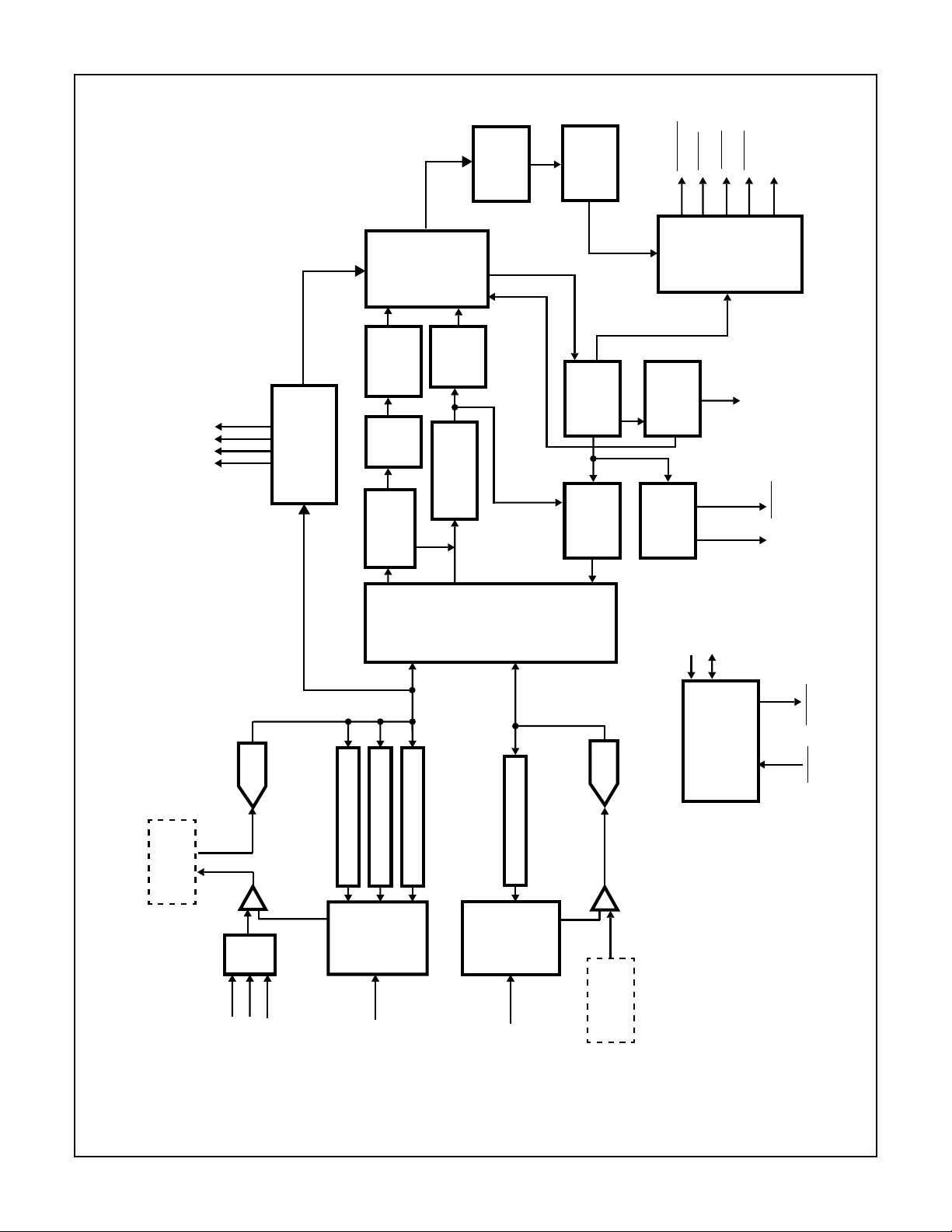
Functional Block Diagram
HMP8116
RATE
OUTPUT
SAMPLE
CONVERTER
USER
ADJUST.
RGB
LOGIC
VBIVALID
HSYNC
BLANK
TIMING
OUTPUT
AND
DVALID
FIFO
P[15:0]
VBI STATUS BITS
ADC
8-BIT
VBI
DETECTION &
DECODING LOGIC
USER
ADJUST
TRAP
COLOR
Y/C
SEPARATION
COLOR
ADJUST
COLOR
DEMODULATION
INPUT
RATE
SAMPLE
CONVERTER
HSYNC
DETECT
PLL
CHROMA
ADC
8-BIT
LINE
LOCK
VSYNC
DETECT
PLL
SCL
SDA
CONTROL
INTERFACE AND
MICROPROCESSOR
LOCKED
VSYNC
FIELD
INTREQ
RESET
FILTER
EXTERNAL
ANTIALIASING
YIN
YOUT
CVBS1
-
+
MUX
INPUT
CVBS2
CVBS3/(Y)
BLACK LEVEL
WHITE PEAK LEVEL
DIGITAL COMPARATORS
AND
AGC
CLAMP
L_CAP
SYNC LEVEL
LOGIC
3
DIGITAL COMPARATOR
LOGIC
CLAMP
CLAMP
AND
GAIN
C_CAP
CONTROL
-
+
C
FILTER
EXTERNAL
ANTIALIASING

Functional Block Diagram
(Continued)
CLK
CHROMA
PLL NCO
CLK TO
4FSC RATIO
C,CVBS
DAT A
LINE
DELAY
COMB
FILTER
CHROMA
PLL LOOP
FILTER
C DATA
DEMODULATOR
CHROMA
CR[7:0]
C
M
U
X
C,CVBS
DAT A
(24.54, 27.0 or 29.5MHz)
4FSC
CLOCK
4
INPUT
SAMPLE
RATE
Y,CVBS
CONVERTER
Y DATA
Y DATA
Y DATA
M
U
X
Y DATA
HUE
ADJUST
AGC
ADJUST
U,V
HORIZONTAL
AND VERTICAL
SHARPNESS
ADJUST
CHROMA
PHASE
DETECTOR
SATURATION
ADJUST
CHROMA
TRAP
VSYNC
DETECT
U, V TO CbCr
COLOR
SPACE
CONVERTER
AND COLOR
KILLER
FIELD
VSYNC
GENLOCK LOSS
LP FILTER
ENABLE
LINE LOCKED
PLL LOOP FILTER
LINE LOCKED
NCO
CbCr
OUTPUT
SAMPLE
RATE
CONVERTER
Y
HSYNC
DETECT
HSYNC
LOCKED
SYNC
STRIPPER,
BRIGHTNESS,
& CONTRAST
ADJUST
HMP8116
VBI DETECTION
& DECODING LOGIC
SHARPNESS
ADJUST
ENABLE
LP FILTER
ENABLE
M
U
X
HSYNC,VSYNC, BLANK,
FIELD, DVALID, VBIVALID
STANDARD
SELECT
P[15:0]
RGB
LOGIC
MUX MUX
OUTPUT
TIMING
AND
FIFO
HMP8116
Introduction
The HMP8116 is designed to decode baseband composite
or S-video NTSC and PAL signals, and convert them to
either digital YCbCr or RGB data. In addition to performing
the basic decoding operations, the HMP8116 includes hardware to decode different types of VBI data and to generate
digital video patterns for a blue screen, black screen and full
screen color bars.
The digital PLLs are designed to synchronize to all NTSC
and PAL standards. A chroma PLL is used to maintain
chroma lock for demodulation of the color information; a linelocked PLL is used to maintain vertical spatial alignment.
The PLLs are designed to maintain lock even in the event of
VCR headswitches and multipath noise.
The HMP8116 contains two 8-bit A/D converters and an I
2
interface for programming internal registers
External Video Processing
Before a video signal can be digitized the decoder has some
external processing considerations that need to be
addressed. This section discusses those external aspects of
the HMP8116.
ANALOG VIDEO INPUTS
The HMP8116 supports either three composite or two composite and one S-video input.
toration” section. After digitization, sample rate converters and
a comb filter are used to perform color separation and demodulation.
A/D CONVERSION
Video data is sampled at the CLK2 frequency then processed by the input sample rate converter. The output levels
of the ADC after AGC and DC restoration processing are:
(M) NTSC (B, D, G, H, I, N
(M, N) PAL PAL
white 196 196
black 66 59
blank 56 59
sync 0 0
C
AGC AND DC RESTORATION
The AGC amplifier attenuates or amplifies the analog video
signal to ensure that the blank level generates code 56 or 59
depending on the video standard. The difference from the
ideal blank level of 56 or 59 is used to control the amount of
attenuation or gain of the analog video signal.
DC restoration positions the video signal so that the sync tip
generates a code 0. The internal timing windows for AGC
and DC Restoration are show in Figure 3.
)
C
Three analog video inputs (CVBS 1-3) are used to select
which one of three composite video sources are to be
decoded. To support S-video applications, the Y channel
drives the CVBS 3 analog input, and the C channel drives
the C analog input.
The analog inputs must be AC-coupled to the video signals,
as shown in the Applications section.
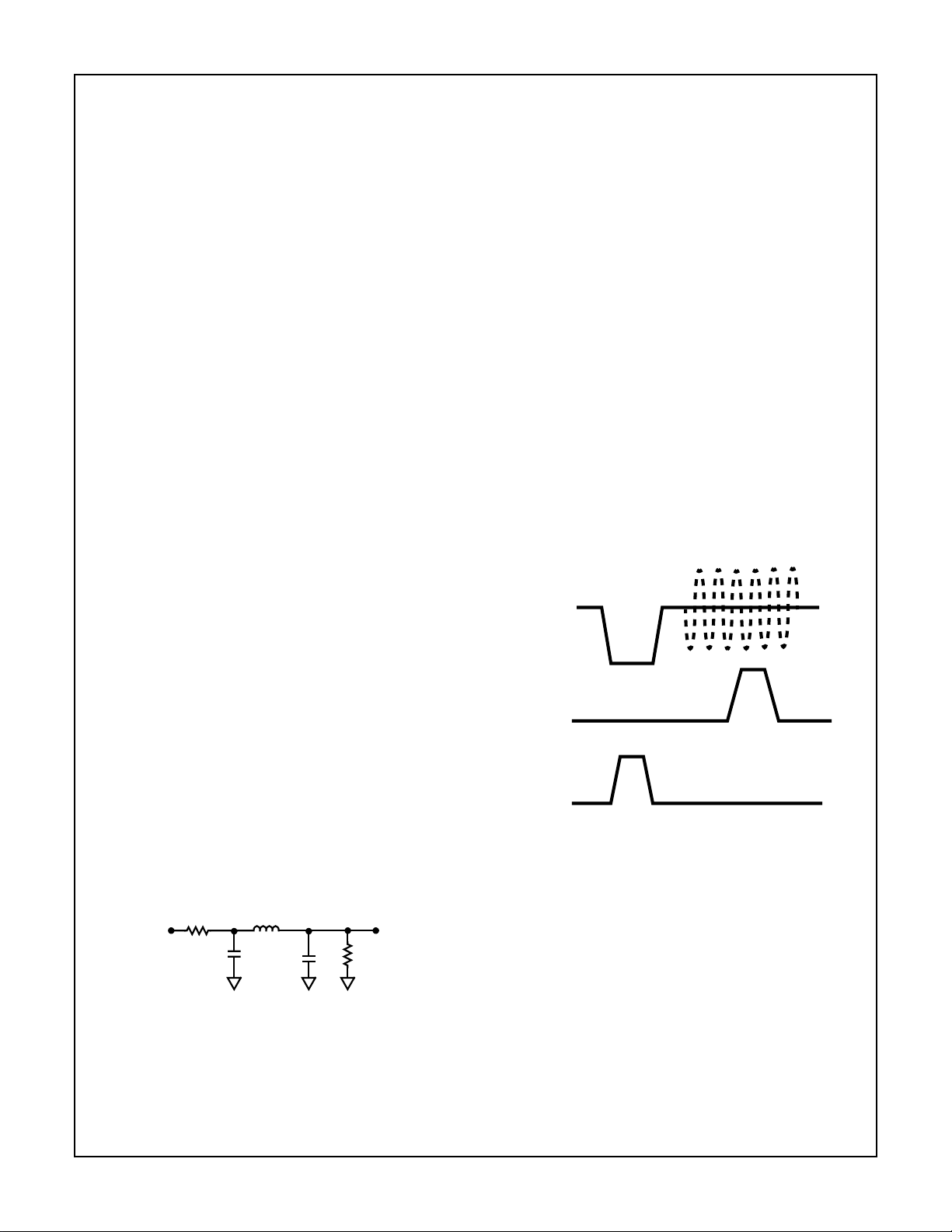
ANTI-ALIASING FILTERS
An external anti-alias filter is required to achieve optimum
performance and prevent high frequency components from
being aliased back into the video image.
For the CVBS 1-3 inputs, a single filter is connected between
the YOUT and YIN pins. For the C input, the antialiasing filter
should be connected before the C input. A recommended filter is shown in Figure 1.
R
YOUT YIN
FIGURE 1. RECOMMENDED ANTI-ALIASING FILTER
332
1
C
33pF
L
1
8.2uH
C
1
82pF
2
R
2
4.02K
Digitization of Video
Prior to A/D conversion, the video signal is DC restored and
gained to generate knownvideo levelsinto the digital processing logic. This process is addessed in the “AGC and DC Res-
VIDEO INPUT
AGC
DC RESTORE
FIGURE 2. AGC AND DC RESTORE INTERNAL TIMING
INPUT SIGNAL DETECTION
It is assumed there is no video input if a horizontal sync is
not detected for 16 consecutive lines. When no video has
been detected, nominal video timing is generated for the
previously detected or programmed video standard. A
maskable interrupt is included to flag when no video has
been detected (bit 6 of the INTERRUPT MASK register 0F
allowing for blue/black/color bar output modes to be enabled
if desired. The vertical sync interrupt can be used in determining when a video signal is present on the currently
selected video mux input. Bit 0 of register 0F
is used to
H
enable vertical sync interrupts.
H
)
5

HMP8116
VERTICAL SYNC AND FIELD DETECTION
The vertical sync and field detect circuit uses a low time
counter to detect the vertical sync sequence in the video
data stream. The low time counter accumulates the low time
encountered during any sync pulse, including serration and
equalization pulses. When the low time count exceeds the
vertical sync detect threshold,
ately. FIELD is asserted at the same time that
VSYNC is asserted immedi-
VSYNC is
asserted. FIELD is asserted low for odd fields and high for
evenfields. Field is determined from the location in the video
line where VSYNC is detected. If VSYNC is detected in the
first half of the line, the field is odd. If VSYNC is detected in
the second half of a line, the field is even.
In the case of lost vertical sync or excessive noise that would
preventthe detection of vertical sync, the FIELD output will continue to toggle. Lost vertical sync is declared if after 337 lines, a
vertical sync period wasnot detectedfor 1 or 3 (selectable)successivefields as specified bybit 2 of the GENLOCK CONTROL
register 04
. When this occurs, the PLLs are initialized to the
H
acquisition state.
Y/C SEPARATION
A composite video signal has the luma (Y) and chroma (C)
information mixed in the same video signal. The Y/C separation process is responsible for separating the composite
video signal into these two components. The HMP8116 utilizes a comb filter to minimize the artifacts that are associated with the Y/C separation process.
INPUT SAMPLE RATE CONVERTER
The input sample rate converter is used to convert video
data sampled at the CLK2 rate to a virtual 4xf
for comb filtering and color demodulation. An interpolating
filter is used to generate the 4xf
samples as illustrated in
SC
Figure 3.
INCOMING VIDEO SAMPLES
sample rate
SC
have a half-line vertical offset from the luma data. This may
be eliminated, vertically aligning the chroma and luma samples, at the expenseof vertical resolution of the luma. Bit 0 of
the OUTPUT FORMAT register 02
controls this option.
H
CHROMA DEMODULATION
The output of the comb filter is further processed using a
patented frequency domain transform to complete the Y/C
separation and demodulate the chromanance.
Demodulation is done at a virtual 4xf
sample rate using
SC
the interpolated data samples to generate U and V data. The
demodulation process decimates by 2 the U/V sample rate.
OUTPUT SAMPLE RATE CONVERTER
The output sample rate converter converts the Y, U and V
data from a virtual 4xf
sample rate to the desired output
SC
sample rate (i.e., 13.5MHz). It also vertically aligns the samples based on the horizontal sync information embedded in
the digital video data stream. The output sample rate is
determined by the selected video standard and whether
square or rectangular pixels are output. The output format is
4:2:2 forall modes exceptthe RGB modes which use a 4:4:4
output format.
CLK2 INPUT
Note that the color subcarrier is derived from CLK2. Any jitter
on CLK2 will be transferred to the color subcarrier, resulting
in color changes. Thus, CLK2 should be derived from a stable clock source, such as a crystal. The use of a PLL to generate CLK2 is not recommended. CLK2 must havea 50ppm
accuracy and at least a 60/40% duty cycle to ensure proper
operation.
The CLK2 clock rate must be one of the following frequencies:
24.54MHz
27.00MHz
29.50MHz
TIME
RESAMPLED VIDEO
TIME
4xf
SC
FIGURE 3. SAMPLE RATE CONVERSION
COMB FILTER
A 2-line comb filter, using a single line delay, is used to perform part of the Y/C separation process. During S-video
operation, the Y signal bypasses the comb filter; the C signal
is processed by the comb filter since it is an integral part of
the chroma demodulator. During PAL operation, the chroma
trap filter should also be enabled for improved performance.
Since a single line store is used, the chroma will normally
The frequency of CLK2 must be 2x the desired output sample rate. The values in table 1 below indicate the CLK2 clock
rate based on the video standard and pixel mode. The output sample rate for the given video standard and pixel mode
is half the CLK2 clock rate.z
TABLE 1. VIDEO STANDARD CLOCKRATE SELECTION
SUMMARY
ALLOWABLE CLK2
FREQUENCIES (MHz)
RECTANGULAR
VIDEO FORMAT
(M) NTSC 27.00 24.54
(B, D, G, H, I, N) PAL 27.00 29.50
(M) PAL 27.00 24.54
(N
) PAL 27.00 29.50
C
PIXEL MODE
SQUARE
PIXEL MODE
6

HMP8116
Digital Processing of Video
Once the luma and chroma have been separated the
HMP8116 then performs programmable modifications (i.e.
contrast, coring, color space conversions, color AGC, etc.) to
the decoded video signal.
UV TO CbCr CONVERSION
The baseband U and V signals are scaled and offset to generate a nominal range of 16-240 for both the Cb and Cr data.
DIGITAL COLOR GAIN CONTROL
There are four types of color gain control modes available:
no gain control, automatic gain control, fixed gain control,
and freeze automatic gain control.
If “no gain control” is selected, the amplitude of the color difference signals (CbCr) is not modified, regardless of variations in the color burst amplitude. Thus, a gain of 1x is
always used for Cb and Cr.
If “automatic gain control” is selected, the amplitude of the
color difference signals (CbCr) is compensated for variations
in the color burst amplitude. The burst amplitude is averaged
with the two previous lines having a color burst to limit lineto-line variations. A gain of 0.5x to 4x is used for Cb and Cr.
If “fixed gain control” is selected, the amplitude of the color
difference signals (CbCr) is multiplied by a constant, regardless of variations in the color burst amplitude. The constant
gain value is specified by the COLOR GAIN register 1C
gain of 0.5x to 4x is used for Cb and Cr. Limiting the gain to
4x limits the amount of amplified noise.
If “freeze automatic gain control” is selected, the amplitude
of the color difference signals (CbCr) is multiplied by a constant. This constant is the value the AGC circuitry generated
when the “freeze automatic gain” command was selected.
COLOR KILLER
If “enable color killer” is selected, the color output is turned
off when the running average of the color burst amplitude is
below approximately 25% of nominal for four consecutive
fields. When the running average of the color burst amplitude is aboveapproximately 25% of nominal for four consecutive fields, the color output is turned on. The color output is
also turned off when excessive phase error of the chroma
PLL is present.
If “force color off” is selected, color information is never
present on the outputs.
If “force color on” is selected, color information is present on
the outputs regardless of the color burst amplitude or
chroma PLL phase error.
Y PROCESSING
The black level is subtracted from the luminance data to
remove sync and any blanking pedestal information. Negative values of Y are supported at this point to allow proper
decoding of “below black” luminance levels.
Scaling is done to position black at 8-bit code 0 and white at
.A
H
8-bit code 219.
A chroma trap filter may be used to remove any residual
color subcarrier from the luminance data. The center frequency of the chroma trap is automatically determined from
the video standard being decoded. The chroma trap should
be disabled during S-video operation to maintain maximum
luminance bandwidth. Alternately, a 3MHz lowpass filter may
be used to remove high-frequency Y data. This may make a
noisy image more pleasing to the user, although softer.
Coring of the high-frequency Y data may be done to reduce
low-level high frequency noise.
Coring of the Y data may also be done to reduce low-level
noise around black. This forces Y data with the following values to a value of 0:
coring = 1: +/- 1
coring = 2: +/- 1, +/- 2
coring = 3: +/- 1, +/- 2. +/- 3
High-frequency components of the luminance signal may be
“peaked” to control the sharpness of the image. Maximum
gain may be selected to occur at either 2.6MHz or the color
subcarrier frequency. This may be used to make the displayed image more pleasing to the user. It should not be
used if the output video will be compressed, as the circuit
introduces high-frequency components that will reduce the
compression ratio.
The brightness control adds or subtracts a user-specified
DC offset to the Y data. The contrast control multiplies the Y
data by a user-specified amount. These may be used to
make the displayed image more pleasing to the user.
Finally, a value of 16 is added to generate a nominal range of
16 (black) to 235 (white).
CbCr PROCESSING
The CbCr data is lowpass filtered to either 0.85 or 1.5MHz.
Coring of the CbCr data may be done to reduce low-level
noise around zero. This forces CbCr data with the following
values to a value of 128.
coring = 1: 127, 129
coring = 2: 126, 127, 129, 130
coring = 3: 125, 126, 127, 129, 130, 131
The saturation control multiplies the CbCr data by a userspecified amount. This may be used to make the displayed
image more pleasing to the user. The CbCr data may also
be optionally multiplied by the contrast value to avoid color
shifts when changing contrast.
The hue control provides a user-specified phase offset to the
color subcarrier during decoding. This may be used to correct slight hue errors due to transmission.
YCbCr OUTPUT FORMAT PROCESSING
Y has a nominal range of 16 to 235. Cb and Cr have a nominal range of 16 to 240, with 128 corresponding to zero. Values less than 1 are made 1 and values greater than 254 are
7

HMP8116
made 254.
BLANK is asserted, Y is forced to have a value of 16,
While
with Cb and Cr forced to have a value of 128, unless VBI
data is present.
RGB OUTPUT FORMAT PROCESSING
The 4:2:2 YCbCr data is converted to 4:4:4 YCbCr data and
then converted to either 15-bit or 16-bit gamma-corrected
RGB (R′G′B′) data. While
forced to a value of 0.
15-Bit R′G′B′
The following YCbCr to R′G′B′ equations are used to maintain the proper black and white levels:
R′ = 0.142(Y - 16) + 0.194(Cr - 128)
G′ = 0.142(Y - 16) - 0.099(Cr - 128) - 0.048(Cb - 128)
B′ = 0.142(Y - 16) + 0.245(Cb - 128)
The resulting 15-bit R′G′B′ data has a range of 0 to 31. Values less than 0 are made 0 and values greater than 31 are
made 31.
The 15-bit R′G′B′ data may be converted to 15-bit linear
RGB, using the following equations. Although the PAL specifications specify a gamma of 2.8, a gamma of 2.2 is normally
used. The HMP8116 allows the selection of the gamma to
be either 2.2 or 2.8, independent of the video standard.
for gamma = 2.2:
for R′G′B′ < 0.0812*31
R = (31)((R′/31)/4.5)
G = (31)((G′/31)/4.5)
B = (31)((B′/31)/4.5)
for R′G′B′ >= 0.0812*31
R = (31)(((R′/31) + 0.099)/1.099)
G = (31)(((G′/31) + 0.099)/1.099)
B = (31)(((B′/31) + 0.099)/1.099)
for gamma = 2.8:
R = (31)(R′/31)
G = (31)(G′/31)
B = (31)(B′/31)
16-Bit R′G′B′
The following YCbCr to R′G′B′ equations are used to maintain the proper black and white levels:
R′ = 0.142(Y - 16) + 0.194(Cr - 128)
G′ = 0.288(Y - 16) - 0.201(Cr - 128) - 0.097(Cb - 128)
B′ = 0.142(Y - 16) + 0.245(Cb - 128)
The resulting 16-bit R′G′B′ data has a range of 0 to 31 for R′
and B′, and a range of 0 to 63 for G′. Values less than 0 are
made 0; R′ and B′ values greater than 31 are made 31, G′
values greater than 63 are made 63.
The 16-bit R′G′B′ data may be converted to 16-bit linear
RGB, using the following equations. Although the PAL speci-
BLANK is asserted, RGB data is
2.2
2.2
2.2
2.8
2.8
2.8
fications specify a gamma of 2.8, a gamma of 2.2 is normally
used. The HMP8116 allows the selection of the gamma to
be either 2.2 or 2.8, independent of the video standard.
for gamma = 2.2:
for R′B′ < 0.0812*31, G′ < 0.0812*63
R = (31)((R′/31)/4.5)
G = (63)((G′/63)/4.5)
B = (31)((B′/31)/4.5)
for R′B′ >= 0.0812*31, G′ >= 0.0812*63
R = (31)(((R′/31) + 0.099)/1.099)
G = (63)(((G′/63) + 0.099)/1.099)
B = (31)(((B′/31) + 0.099)/1.099)
2.2
2.2
2.2
for gamma = 2.8:
R = (31)(R′/31)
G = (63)(G′/63)
B = (31)(B′/31)
2.8
2.8
2.8
BUILT-IN VIDEO GENERATION
When the blue screen, black screen or color bar output is
selected, a full-screen of blue, black or 75% colorbar output
is generated using the currently selected output format. The
type of screen to be generated is determined by bits 2 and 1
of the OUTPUT FORMAT register 02
. When built-in video
H
generation is not desired, the bits need to be set for normal
operation to pass decoded video.
If a video source is input, it will be used to provide the video
timing. If an input video source is not detected, internallygenerated video timing will be used.
Pixel Port Timing
The the timing and format of the output data and control signals is presented in the following sections.
HSYNC AND VSYNC TIMING
The HSYNC and VSYNC output timing is VMI v1.4 compatible.Figures 4-7 illustrate the video timing. The leading edge of
HSYNC is synchronous to the video input signal and has a
fixed latency due to internal pipeline processing. The pulse
width of the
36
, where the trailing edge of HSYNC has a programmable
H
delay of 0-510 CLK2 cycles from the leading edge.
The leading edge of
way through the first serration pulse of each field. For an odd
field, the trailing edge of
trailing edge of the
pulse. Refer to Figures 4 and 6. For an even field, the trailing
edge of
of the
Figures 5 and 7.
FIELD TIMING
When field information can be determined from the input
video source, the FIELD output pin reflects the video source
HSYNC is defined by the END HSYNC register
VSYNC is asserted approximately half
VSYNC is 5±1 CLK2 cycles after the
HSYNC that follows the last equalization
VSYNC is 5±1 CLK2 cycles leading the leading edge
HSYNC that follows the last equalization pulse. Refer to
8

HMP8116
field state. When field information cannot be determined
from the input video source, the FIELD output pin alternates
NTSC(M)
LINE #
PAL(M)
LINE #
VIDEO
INPUT
HSYNC
VSYNC
FIELD
1
523
‘EVEN’ FIELD
2345678910525524
5245251234567522521
its state at the beginning of each field. FIELD changes state
±1 CLK2 cycles before the the leading edge of VSYNC.
5
‘ODD’ FIELD
NOTE:
3. The trailing edgeofVSYNCis 5±1 clocks after the trailing edgeof HSYNCtobeVMI compatible and to indicate a transitiontoanodd field.
FIGURE 4. NTSC(M) AND PAL(M) HSYNC, VSYNC AND FIELD TIMING DURING AN EVEN TO ODD FIELD TRANSITION
NTSC(M)
LINE #
PAL(M)
LINE #
VIDEO
INPUT
264
261
265 266 267 268 269 270 271 272 273263262
262 263 264 265 266 267 268 269 270260259
HSYNC
VSYNC
FIELD
‘ODD’ FIELD ‘EVEN’ FIELD
NOTE:
4. The trailing edgeof VSYNC is 5±1 clocks after theleading edge of HSYNC tobe VMI compatible and toindicate a transition to anevenfield.
FIGURE 5. NTSC(M) AND PAL(M) HSYNC, VSYNC AND FIELD TIMING DURING AN ODD TO EVEN FIELD TRANSITION
623LINE # 6246251234567622621
VIDEO
INPUT
HSYNC
VSYNC
FIELD
‘EVEN’ FIELD
‘ODD’ FIELD
NOTE:
5. The trailing edgeofVSYNC is 5±1 clocks after the trailing edgeofHSYNC is to be VMIcompatibleandto indicate a transition to anoddfield.
FIGURE 6. PAL(B,D,G,H,I,N,NC) HSYNC, VSYNC AND FIELD TIMING DURING AN EVEN TO ODD FIELD TRANSITION
9

VIDEO
INPUT
HSYNC
VSYNC
HMP8116
311LINE # 312 313 314 315 316 317 318 319 320310309
FIELD
NOTE:
6. The trailing edgeof VSYNC is 5±1 clocks after theleading edge of HSYNC tobe VMI compatible and toindicate a transition to anevenfield.
FIGURE 7. PAL(B,D,G,H,I,N,NC) HSYNC, VSYNC AND FIELD TIMING DURING AN ODD TO EVEN FIELD TRANSITION
BLANK AND DVALID TIMING
DVALID is asserted when P15-P0 contain valid data. The
timing and behavior of
video format and the programmed values for bit 4
(DVLD_DCYC) and bit 5 (DVLD_LTC) of the GENLOCK
CONTROL register 04
format sections that follow for the specific behavior for
DVALID.
BLANK is used to determine if the HMP8116 is generating
active video data.
DVALID to capture digital data from the decoder. BLANK,
DVALID and the video data are output after the internal pipeline latency and synchronous with the rising edge of CLK2.
VIDEO STANDARD
(MSB/LSB)
DVALID is dependent on the output
. Refer to the specific output video
H
BLANK should be used in conjunction with
ACTIVE
PIXELS/
‘ODD’ FIELD ‘EVEN’ FIELD
During active scan lines
BLANK is negated when the horizontal pixel count matches the value in the END H_BLANK
register 32
. A count of 00Hcorresponds to the 50% point of
H
the leading edge of the sync tip after leaving the part.
BLANK is asserted when the horizontal pixel count matches
the value in the START H_BLANK register 31
that horizontally,
BLANK is programmable with two pixel res-
olution.
START V_BLANK register 34
ister 35
determine which scan lines are blanked for each
H
field. During inactivescan lines,
entire scan line. Half-line blanking of the output video cannot
be done. Reference Figure 8 for active video timing and use
Table 2 for typical blanking programming values
TABLE 2. TYPICAL VALUES FOR HBLANK AND VBLANK REGISTERS
LINE
TOTAL
PIXELS/
LINE
LAST
PIXEL
COUNT
START
H_BLANK
(31H/30H)
END
H_BLANK
(32H)
/30H. Note
H
/33Hand END V_BLANK reg-
H
BLANK is asserted during the
START
V_BLANK
(34H/33H)
END
V_BLANK
(35H)
RECTANGULAR PIXELS
NTSC (M), PAL (M)
PAL (B, D, G, H, I,N, NC)
SQUARE PIXELS
NTSC (M), PAL (M)
PAL (B, D, G, H, I,N, NC)
720
720
640
768
858
864
780
944
857 (0359H)
863 (035FH)
779 (030BH)
943 (03AFH)
842 (034AH)
852 (0354H)
758 (02F6H)
922 (039AH)
122 (7AH)
132 (84H)
118 (76H)
154 (9AH)
259 (0103H)
310 (0136H)
259 (0103H)
310 (0136H)
19 (13H)
22 (16H)
19 (13H)
22 (16H)
10

HMP8116
480 ACTIVE
LINES/FRAME
(NTSC, PAL M)
NTSC M PAL B, D, G, H, I, N, N
LINES 1 - 22 NOT ACTIVE
240 ACTIVE LINES
PER FIELD
(LINES 23-262)
LINES 263 - 284 NOT ACTIVE
240 ACTIVE LINES
PER FIELD
(LINES 285 - 524)
LINE 525
NOT ACTIVE
TOTAL PIXELS
ACTIVE PIXELS
ODD FIELD
SYNC AND
PORCH
VERTICAL
BLANKING
EVEN FIELD
FRONT
PORCH
NUMBER OF PIXELS
RECTANGULAR (SQUARE)
NTSC PAL
858
720
(780)
(640)
864
720
BACK
(944)
(768)
LINES 1 - 22 NOT ACTIVE
288 ACTIVE LINES
PER FIELD
(LINES 23 - 310)
LINES 311 - 335 NOT ACTIVE
288 ACTIVE LINES
PER FIELD
(LINES 336 - 623)
LINES 624-625
NOT ACTIVE
TOTAL PIXELS
ACTIVE PIXELS
C
576 ACTIVE
LINES/FRAME
(PAL)
NOTE:
7. The line numbering for PAL (M) followings NTSC (M) line count minus 3 per the video standards.
FIGURE 8. TYPICAL ACTIVE VIDEO REGIONS
TABLE 3. PIXEL OUTPUT FORMATS
PIN NAME 8-BIT, 4:2:2, YCbCr 16-BIT, 4:2:2, YCbCr 15-BIT, RGB, (5,5,5) 16-BIT, RGB, (5,6,5) BT.656
P0
P1
P2
P3
P4
P5
P6
P7
P8
P9
P10
P11
P12
P13
P14
P15
0 [0]
0 [0]
0 [0]
0 [0]
0 [0]
0 [0]
0 [0]
0 [0]
Y0, Cb0, Cr0 [D0]
Y1, Cb1, Cr1 [D1]
Y2, Cb2, Cr2 [D2]
Y3, Cb3, Cr3 [D3]
Y4, Cb4, Cr4 [D4]
Y5, Cb5, Cr5 [D5]
Y6, Cb6, Cr6 [D6]
Y7, Cb7, Cr7 [D7]
Cb0, Cr0 [D0
Cb1, Cr1 [D1
Cb2, Cr2 [D2
Cb3, Cr3 [D3
Cb4, Cr4 [D4
Cb5, Cr5 [D5
Cb6, Cr6 [D6
Cb7, Cr7 [D7
Y0 [D0n]
Y1 [D1n]
Y2 [D2n]
Y3 [D3n]
Y4 [D4n]
Y5 [D5n]
Y6 [D6n]
Y7 [D7n]
n+1
n+1
n+1
n+1
n+1
n+1
n+1
n+1
]
]
]
]
]
]
]
]
B0 [D0
B1 [D1
B2 [D2
B3 [D3
B4 [D4
G0 [D5
G1 [D6
G2 [D7
G3 [D0n]
G4 [D1n]
R0 [D2n]
R1 [D3n]
R2 [D4n]
R3 [D5n]
R4 [D6n]
0 [D7n]
n+1
n+1
n+1
n+1
n+1
n+1
n+1
n+1
]
]
]
]
]
]
]
]
B0 [D0
B1 [D1
B2 [D2
B3 [D3
B4 [D4
G0 [D5
G1 [D6
G2 [D7
G3 [D0n]
G4 [D1n]
G5 [D2n]
R0 [D3n]
R1 [D4n]
R2 [D5n]
R3 [D6n]
n+1
n+1
n+1
n+1
n+1
n+1
n+1
n+1
]
]
]
]
]
]
]
]
0 [0]
0 [0]
0 [0]
0 [0]
0 [0]
0 [0]
0 [0]
0 [0]
YCbCr Data,
Ancillary Data,
SAV and EAV
Sequences
[D0 - D7, where
P8 corresponds
to D0]
R4 [D7n]
NOTE:
8. Definitions in brackets are port definitions duringraw VBI data transfers. Refer to the sectionon teletext for more information on raw VBI.
PIXEL OUTPUT PORT
Pixel data is output via the P0-P15 pins. Refer to Table 3 for
the output pin definition as a function of the output mode.
8-BIT YCbCr OUTPUT
The DVALID output pin may be configured to operate in one
of two ways. The configuration is determined by the
DVLD_LTC bit (bit 4) of the GENLOCK CONTROL register
04
.
H
If DVLD_LTC=0, the
during the entire active video time on active scan lines if CLK2
is exactly 2x the desired output sample rate.
DVALID output is continuously asserted
DVALID being
asserted indicates valid pixel data is present on the P15-P8
pixel outputs.
DVALID is never asserted during the blanking
intervals. Refer to Figure 9.
If DLVD_LTC=1,
DVALID has the same internal timing as the
first mode, but is ANDed with the CLK2 signal, and the result
is output onto the
DVALID pin. This results in a gated CLK2
signal being output during the active video time on active
scan lines. Refer to Figure 10.
If 8-bit YCbCr data is generated, it is output following each
rising edge of CLK2. The YCbCr data is multiplexed as [Cb Y
Cr Y′ CbYCrY′...], with the first active data each scan line
containing Cb data. The pixel output timing is shown in Fig-
11

HMP8116
ures 9 and 10.
BLANK, HSYNC, VSYNC, DVALID, VBIVALID, and FIELD
are output following the rising edge of CLK2. When
CLK
DVALID
BLANK
P[15-8]
NOTE:
t
DVLD
Cb
Y
0
0
BLANK
Cr
0
is asserted and
have a value of 16 for Y and 128 for Cb and Cr .
Y
Cb
1
2
VBIVALID is deasserted, the YCbCr outputs
Y
2
Cr
Y
2
3
Cb
Y
4
4
9. Y0is the first active luminance pixel data of a line. Cb0and Cr0are first active chrominance pixel data in a line. Cb and Cr will alternate
every cycle due to the 4:2:2 subsampling. Pixel data is not output during the blanking period, but the values on the ports are forced to
blanking levels.
FIGURE 9. OUTPUT TIMING FOR 8-BIT YCbCr MODE (DVLD_LTC = 0)
CLK
DVALID
BLANK
P[15-8]
NOTES:
t
DVLD
Cb
Y
0
0
Cr
Y
0
Cb
1
Y
2
2
Cr
Y
2
Cb
3
Y
4
4
10. Y0is the first active luminance pixel data of a line. Cb0and Cr0are first active chrominance pixel data in a line. Cb and Cr will alternate
every cycle due to the 4:2:2 subsampling. Pixel data is not output during the blanking period, but the values on the ports are forced to
blanking levels.
11. When DVLD_LTCis set to 1, the polarity ofDVALIDneeds to be set to active low,otherwise DVALID will stay lowduring active video and
be gated with the clock only during the blanking interval.
FIGURE 10. OUTPUT TIMING FOR 8-BIT YCbCr MODE (DVLD_LTC = 1)
16-BIT YCbCr, 15-BIT RGB, OR 16-RGB OUTPUT
In these output modes, DVALID may be configured to operate in one of four modes as controlled by the DVLD_LTC and
DVLD_DCYC bits of the GENLOCK CONTROL register
(04
). Bit 4 is the DVLD_LTC bit and bit 5 is the
H
DVLD_DCYC bit.
If DVLD_LTC=0 and DVLD_DCYC=0 ,
only during the active video time on active scan lines. Thus,
DVALID being asserted indicates valid pixel data is present
on the P0-P15 pixel outputs.
DVALID is never asserted during the blanking intervals. In this mode
50% duty cycle only during the active video times. The timing diagrams for this mode can be found in figures 11 and
12.
DVALID is present
DVALID will have a
same as the first mode, with the exception that
not have a 50% duty cycle. This mode is intended for backward compatibility with HMP8112(A) timing dependancies in
which
DVALID did not have a 50% duty cycle timing and
other timing variations. The timing diagrams for this mode
can be found in figures 13 and 14.
If DVLD_LTC=1 and DVLD_DCYC=0,
entire line time on all scan lines.
DVALID is present the
DVALID may occasionally
be negated for two consecutive CLK2 cycles just prior to
active video. In this mode
DVALID is guaranteed havea 50%
duty cycle only during the active video times. The timing for
this mode differs from the timing shown in figures 11 and 12
only in that
DVALID will also be asserted during the blanking
portion of the video line time as described above.
DVALID does
If DVLD_LTC=0 and DVLD_DCYC=1,
DVALID behaves the
12

HMP8116
If DVLD_LTC=1 and DVLD_DCYC=1,
during the entire line time on all scan lines.
DVALID is present
DVALID is
asserted during the blankingintervals as needed to ensure a
constant number of total samples per line. The timing for this
mode differs from the timing shown in figures 13 and 14 only
in that
DVALID will also be asserted during the blanking por-
tion of the video line time as described above.
If 16-bit YCbCr, 15-bit RGB data, or 16-bit RGB data is gen-
erated, it is output following the rising edge of CLK2 while
CLK
DVALID
BLANK
Cb
Y
0
0
Y
1
Cr
0
P15-P8
P7-P0
DVALID is asserted. Either linear or gamma-corrected RGB
data may be output. The pixel output timing is shown in Figures 11 to 14.
BLANK, HSYNC, VSYNC, DVALID, VBIVALID, and FIELD
are output following the rising edge of CLK2. When
is asserted and
VBIVALID is deasserted, the YCbCr outputs
BLANK
havea value of 16 forY and 128 for Cb and Cr; the RGB outputs have a value of 0.
Cb
Y
2
2
Y
3
Cr
2
Cb
Y
4
4
t
DVLD
NOTES:
12. Y0is the first active luminance pixel data of a line. Cb0and Cr0are first active chrominance pixel data in a line. Cb and Cr will alternate
every cycle due to the 4:2:2 subsampling.
13. BLANK is asserted per Figure 8.
FIGURE 11. OUTPUT TIMING FOR 16-BIT YCbCr MODE (DVLD_LTC = 0, DVLD_DCYC = 0)
CLK
DVALID
P15-P11
[P14-P10]
P10-P5
[P9-P5]
P4-P0
R
0
G
0
B
0
R
1
G
1
B
1
R
2
G
2
B
2
R
3
G
3
B
3
R
4
G
4
B
4
t
NOTE:
BLANK is asserted per Figure 8.
14.
DVLD
FIGURE 12. OUTPUT TIMING FOR 16-BIT [15-BIT] RGB MODE (DVLD_LTC = 0, DVLD_DCYC = 0)
13
 Loading...