

Intersil Corporation HMA510 Datasheet

April 1997
HMA510
16 x 16-Bit CMOS Parallel
Multiplier Accumulator
Features
• 16 x 16-Bit Parallel Multiplication with Accumulation
to a 35-Bit Result
• High-Speed (45ns) Multiply Accumulate Time
• Low Power CMOS Operation
-I
-I
= 500µA Maximum
CCSB
= 7.0mA Maximum at 1.0MHz
CCOP
• HMA510 is Compatible with the CY7C510 and the
IDT7210
• Supports Two’s Complement or Unsigned Magnitude
Operations
• TTL Compatible Inputs/Outputs
• Three-State Outputs
Ordering Information
TEMP. RANGE
PART NUMBER
HMA510JC-45 0 to 70 68 Ld PLCC N68.95
HMA510JC-55 0 to 70 68 Ld PLCC N68.95
HMA510GC-55 0 to 70 68 Ld CPGA G68.B
(oC) PACKAGE
PKG.
NO.
Description
The HMA510 is a high speed, low power CMOS 16 x 16-bit
parallel multiplier accumulator capable of operating at 45ns
clocked multiply-accumulate cycles. The 16-bit X and Y
operands may be specified as either two’s complement or
unsigned magnitude format. Additional inputs are provided
for the accumulator functions which include: loading the
accumulator with the current product, adding or subtracting
the accumulator contents and the current product, and preloading the Accumulator Registers from the external inputs.
All inputs and outputs are registered. The registers are all
positive edge triggered, and are latched on the rising edge of
the associated clock signal. The 35-bit Accumulator Output
Register is broken into three parts. The 16-bit least significant product (LSP), the 16-bit most significant product
(MSP), and the 3-bit extended product (XTP) Registers. The
XTP and MSP Registers have dedicated output ports, while
the LSP Register shares the Y-inputs in a multiplexed fashion. The entire 35-bit Accumulator Output Register may be
preloaded at any time through the use of the bidirectional
output ports and the preloaded control.
Block Diagram
PRELOAD
CLKP
X0-15
TC
REGISTER
CLKY
CLKX
MULTIPLIER ARRAY
ACCUMULATOR
XTP REGISTER MSP REGISTER LSP REGISTER
3
OEX
OEM
OEL
P32-34
SUB
RND
ACC
REGISTER REGISTER
35
P16-31
Y0-15 P0-15
1616
16
35
16
CAUTION: These devices are sensitive to electrostatic discharge; follow proper IC Handling Procedures.
http://www.intersil.com or 407-727-9207
| Copyright © Intersil Corporation 1999
3-1
File Number 2806.2
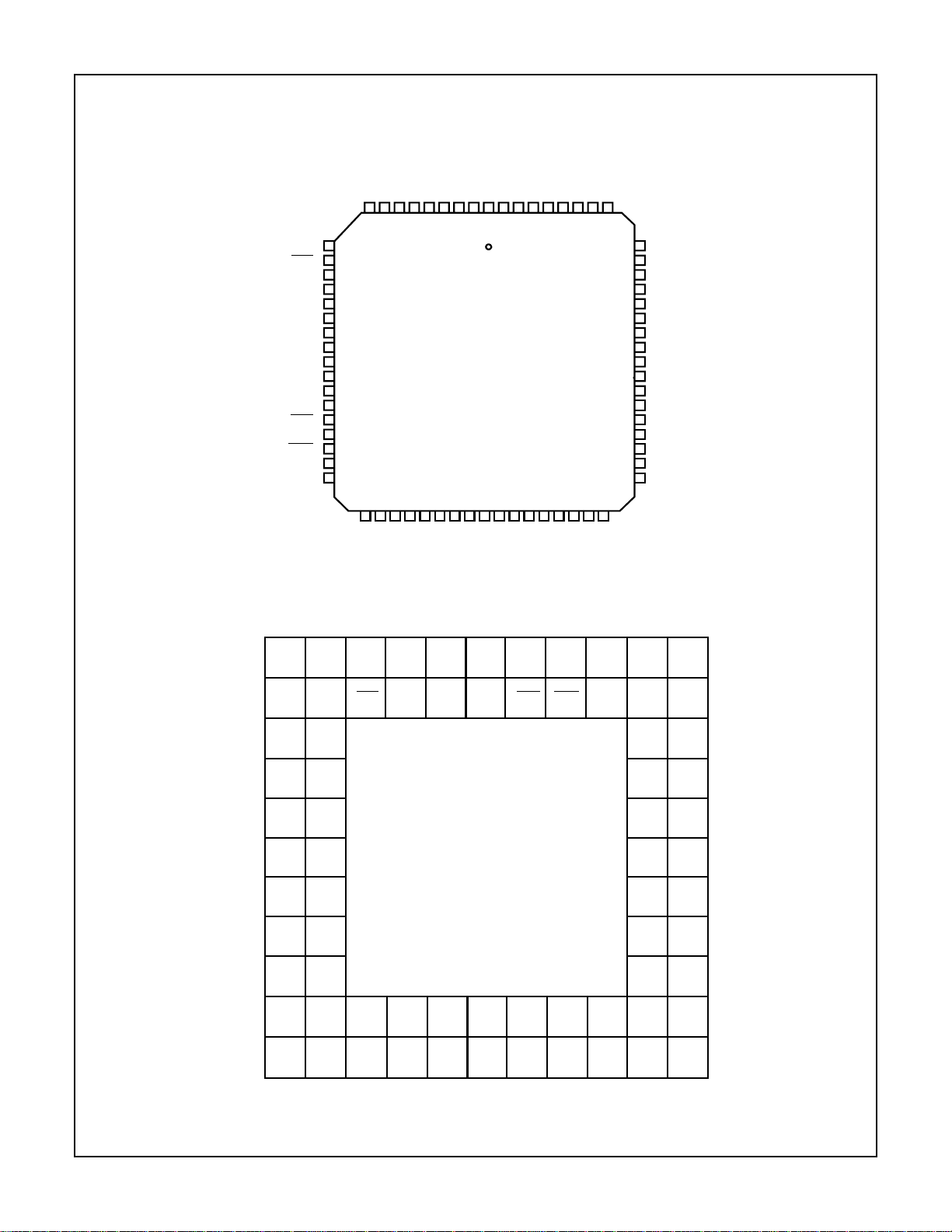
Pinouts
X15
OEL
RND
SUB
ACC
CLKX
CLKY
V
CC
V
CC
V
CC
V
CC
TC
OEX
PREL
OEM
CLKP
P34
X12
X13
X14
10
11
12
13
14
15
16
17
18
19
20
21
22
23
24
25
26
27 28 29 30 31 32 33
HMA510
68 LEAD PLCC
TOP VIEW
X11
X10X9X8X7X6X5X4X3X2X1X0
123456789
68 67 66 65 64 63 62 61
Y0/P0
Y1/P1
43424140393837363534
Y2/P2
60
Y3/P3
59
Y4/P4
58
Y5/P5
57
Y6/P6
56
Y7/P7
55
GND
54
GND
53
Y8/P8
52
Y9/P9
51
Y10/P10
50
Y11/P11
49
Y12/P12
48
Y13/P13
47
Y14/P14
46
Y15/P15
45
P16
44
P33
P32
P31
P30
P29
P28
P27
P26
P25
P24
P23
P22
P21
P20
P19
P17
P18
68 LEAD CPGA
TOP VIEW
X15
X13
X11
X9
X7
X5
X3
X1
N/C
X14
X12
X10
X8
X6
X4
X2
X0
11
10
9
8
7
6
5
4
Y0/P0
3
OEL
RND
SUB
ACC
CLKX
CLKY
V
CC
TC
OEX
PREL
OEM
CLKP
P34
P33
P32
P30
P28
P26
P24
P22
P20
P18
N/C
P31
P29
P27
P25
P23
P21
P19
N/C
2
1
Y1/P1
Y3/P3
Y2/P2
Y4/P4
BA KLCD E F GH J
Y5/P5
Y6/P6
Y7/P7
GND
Y8/P8
Y9/P9
Y10/
P10 P12 P14
Y11/
P11 P13 P15
Y12/
Y13/
Y14/
Y15/
P16
N/C
P17
3-2

Pin Descriptions
PLCC PIN
NAME
NUMBER TYPE DESCRIPTION
HMA510
V
CC
GND 53, 54 The device ground.
X0-X15 1-10, 63-68 I X-Input Data. These 16 data inputs provide the multiplicand which may be in two's com-
Y0-Y15/
P0-P15
P16-P3 29-44 I/O MSP Output Data. This 16-bit port is used to provide the Most Significant Product Out-
P32-P34 26-28 I/O XTP Output Data. This 3-bit port is used to provide the Extended Product Output (P32-
TC 21 I Two's Complement Control. Input data is interpreted as two's complement when this
ACC 14 I Accumulate Control. When this control is HIGH, the Accumulator Output Register con-
SUB 13 I Subtract Control. When both SUB and ACC are HIGH, the Accumulator Register con-
17-20 The +5V power supply pins. 0.1µF capacitors between the VCC and GND pins are rec-
ommended.
plement or unsigned magnitude format.
45-52, 55-62 I/O Y-Input/LSP Output Data. This 16-bit port is used to provide the multiplier which may
be in two's complement or unsigned magnitude format. It may also be used for output
of the Least Significant Product (P0-P15) or for preloading the LSP Register.
put (P16-P31). It may also be used to preload the MSP Register.
P34). It may also be used to preload the XTP Register.
control is HIGH. A LOW indicates the data is to be interpreted as unsigned magnitude
format. This control is latched on the rising edge of CLKX or CLKY.
tents are added to or subtracted from the current product, and the result is stored back
into the accumulator Output Register.
When LOW, the product is loaded into the accumulator Output Register overwriting the
current contents. This control is also latched on the rising edge of CLKX or CLKY.
tents are subtracted from the current product. When ACC is HIGH and SUB is LOW,
the Accumulator Register contents and the current product are summed. The SUB control input is latched on the rising edge of CLKX or CLKY.
RND 12 I Round Control. When this control is HIGH, a one is added to the most significant bit of
the LSP. When LOW, the product is unchanged.
PREL 23 I Preload Control. When this control is HIGH, the three bidirectional ports may be used
to preload the Accumulator Registers. The three-state controls (OEX, OEM, OEL) must
be HIGH, and the data will be preloaded on the rising edge of CLKP. When this control
is LOW, the Accumulator Registers function in a normal manner.
OEL 11 I Y-Input/LSP Output Port Three-State Control. When OEL is HIGH, the output drivers
are in the high impedance state. This state is required for Y-data input or preloading the
LSP Register. When OEL is LOW, the port is enabled for LSP output.
OEM 24 I MSP Output Port Three-State Control. A LOW on this control line enables the port for
output. When OEM is HIGH, the output drivers are in the high impedance state.
This control must be HIGH for preloading the MSP Register.
OEX 22 I XTP Output Port Three-State Control. A LOW on this control line enables the port for
output. When OEX is HIGH, the output drivers are in the high impedance state. This
control must be HIGH for preloading the XTP Register.
CLKX 15 I X-Register Clock. The rising edge of this clock latches the X-Data Input Register along
with the TC, ACC, SUB and RND inputs.
CLKY 16 I Y-Register Clock. The rising edge of this clock latches the Y-Data Input Register along
with the TC, ACC, SUB and RND inputs.
CLKP 25 I Product Register Clock. The rising edge of CLKP latches the LSP, MSP and XTP Reg-
isters. If the preload control is active, the data on the I/O ports is loaded into these registers. If preload is not active, the accumulated product is loaded into the registers.
3-3
 Loading...