

®
www.BDTIC.com/Intersil
HM-6642/883
Data Sheet March 2004
512 x 8 CMOS PROM
The HM-6642/883 is a 512 x 8 CMOS NiCr fusible link
Programmable Read Only Memory in the popular 24 pin,
byte wide pinout. Synchronous circuit design techniques
combine with CMOS processing to give this device high
speed performance with very low power dissipation.
On-chip address latches are provided, allowing easy
interfacing with recent generation microprocessors that use
multiplexed address/data bus structures, such as the 8085.
The output enable controls, both active low and active high,
further simplify microprocessor system interfacing by
allowing output data bus control independent of the chip
enable control. The data output latches allow the use of the
HM-6642/883 in high speed pipelined architecture systems,
and also in synchronous logic replacement functions.
Applications for the HM-6642/883 CMOS PROM include low
power hand held microprocessor based instrumentation and
communications systems, remote data acquisition and
processing systems, processor control store, and
synchronous logic replacement.
FN3013.2
Features
• This Circuit is Processed in Accordance to MIL-STD-883
and is Fully Conformant Under the Provisions of
Paragraph 1.2.1.
• Low Power Standby and Operating Power
- ICCSB. . . . . . . . . . . . . . . . . . . . . . . . . . . . . . . . . .100µA
- ICCOP . . . . . . . . . . . . . . . . . . . . . . . . . . 20mA at 1MHz
• Fast Access Time. . . . . . . . . . . . . . . . . . . . . . . 120/200ns
• Wide Operating . . . . . . . . . . . . . . . . . . . .-55°C to +125°C
• Temperature Range
• Industry Standard Pinout
• Single 5.0V Supply
• CMOS/TTL Compatible Inputs
• Field Programmable
• Synchronous Operation
• On-Chip Address Latches
• Separate Output Enable
All bits are manufactured storing a logical “0” and can be
selectively programmed for a logical “1” at any bit location.
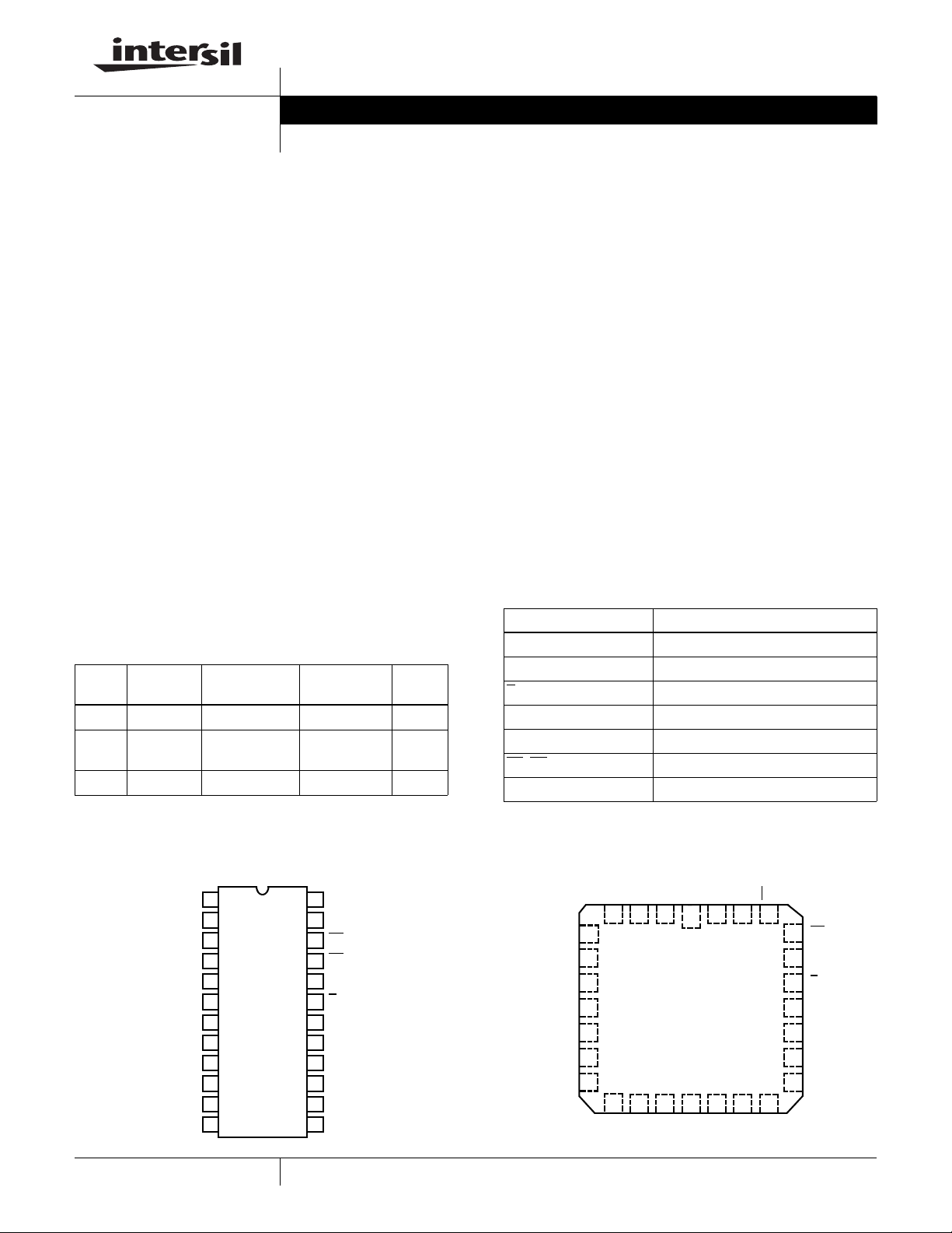
Ordering Information
TEMP.
PKG.
RANGE (°C) 120ns 200ns
SBDIP -55 to +125 HM1-6642B/883 HM1-6642/883 D24.6
SLIM
-55 to +125 HM6-6642B/883 HM6-6642/883 D24.3
SBDIP
CLCC -55 to +125 - HM4-6642/883 J28.A
PKG.
DWG. #
Pinouts
M-6642/883 (SBDIP)
TOP VIEW
A7
A6
A5
A4
A3
A2
A1
A0
Q0
Q1
Q2
GND
1
2
3
4
5
6
7
8
9
10
11
12
24
V
CC
A8
23
22
G1
21
G2
20
G3
E
19
P
18
17
Q7
Q6
16
Q5
15
Q4
14
Q3
13
Pin Description
PIN DESCRIPTION
NC No Connect
A0-A8 Address Inputs
E
Q Data Output
V
Power (+5V)
CC
, G2, G3 Output Enable
G1
P (Note) Program Enable
NOTE: P should be hardwired to GND except during programming.
A4
5
A3
6
A2
7
A1
8
9
A0
NC
10
Q0
11
Chip Enable
HM-6642/883 (CLCC)
TOP VIEW
A5
A6
A7
NC
3 2 14
14 15 16 17 1812 13
Q1
Q2
GND
NC
CC
A8
V
28 27 26
Q3Q5Q4
G1
25
G2
24
G3
E
23
22
P
21
NC
20
Q7
19
Q6
1
CAUTION: These devices are sensitive to electrostatic discharge; follow proper IC Handling Procedures.
1-888-INTERSIL or 321-724-7143
| Intersil (and design) is a registered trademark of Intersil Americas Inc.
All other trademarks mentioned are the property of their respective owners.
Copyright © Intersil Americas Inc. 2004. All Rights Reserved
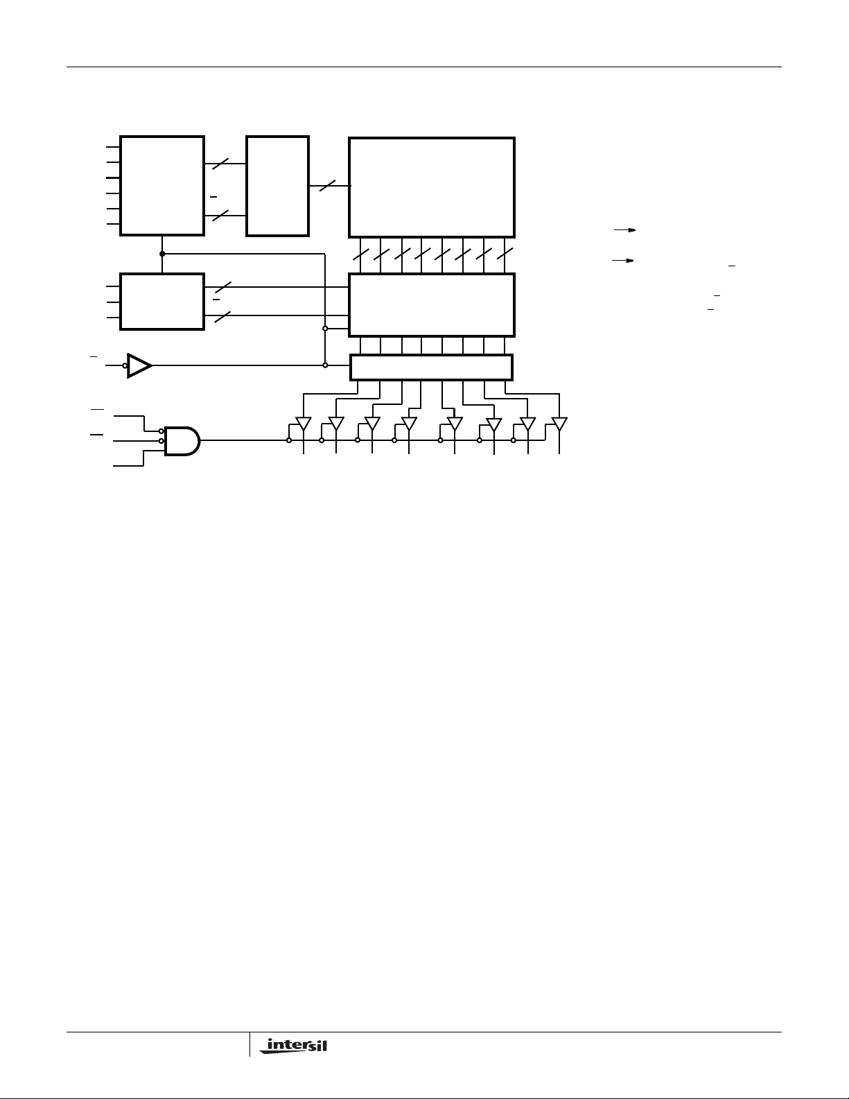
Functional Diagram
www.BDTIC.com/Intersil
HM-6642/883
A8
A7
A6
A5
A4
A3
A2
A1
A0
E
G1
G2
G3
LATCHED
ADDRESS
REGISTER
LATCHED
ADDRESS
REGISTER
A
6
GATED
ROW
A
DECODER
6
A
3
A
3
64
8 8
D
Q0 Q1 Q2 Q3 Q4 Q5 Q6 Q7
64 x 64
MATRIX
8 8
8 8
GATED COLUMN
DECODER
8-BIT DATA LATCH
ALL LINES POSITIVE LOGIC - ACTIVE HIGH
THREE STATE BUFFERS:
A HIGH
DATA LATCHES:
8
8
L HIGH
Q LATCHES ON RISING EDGE OF E
ADDRESS LATCHES AND GATED DECODERS:
LATCH ON FALLING EDGE OF E
GATE ON FALLING EDGE OF E
P SHOULD BE HARDWIRED TO GND EXCEPT
DURING PROGRAMMING
OUTPUT ACTIVE
Q = D
2
HM-6642/883
www.BDTIC.com/Intersil
Absolute Maximum Ratings Thermal Information
Supply Voltage. . . . . . . . . . . . . . . . . . . . . . . . . . . . . . . . . . . . . +7.0V
Input, Output or I/O Voltage. . . . . . . . . . . . GND-0.3V to VCC+0.3V
Typical Derating Factor . . . . . . . . . . . 5mA/MHz Increase in ICCOP
ESD Classification . . . . . . . . . . . . . . . . . . . . . . . . . . . . . . . . .Class 1
Operating Conditions
Operating Voltage Range . . . . . . . . . . . . . . . . . . . . . . . . +4.5V to +5.5V
Operating Temperature Range . . . . . . . . . . . . . . . .-55°C to +125°C
Input Low Voltage . . . . . . . . . . . . . . . . . . . . . . . . . . . -0.3V to +0.8V
Input High Voltage . . . . . . . . . . . . . . . . . . . . . . . . . 2.4 to VCC+0.3V
CAUTION: Stresses above those listed in “Absolute Maximum Ratings” may cause permanent damage to the device. This is a stress only rating and operation of the
device at these or any other conditions above those indicated in the operational sections of this specification is not implied.
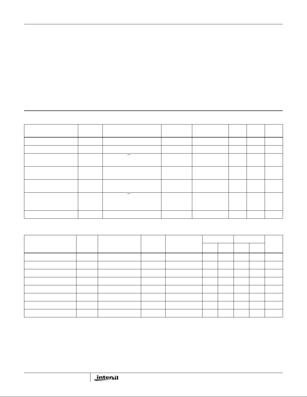
TABLE 1. HM-6642/883 DC ELECTRICAL PERFORMANCE SPECIFICATIONS
Device Guaranteed and 100% Tested
(NOTES 1, 4)
PARAMETER SYMBOL
High Level Output Voltage VOH VCC = 4.5V, IO = -1.0mA 1, 2, 3 -55 ≤ T
Low Level Output Voltage VOL VCC = 4.5V, IO = +3.2mA 1, 2, 3 -55 ≤ TA ≤ +125 - 0.4 V
High Impedance Output
Leakage Current
Input Leakage Current II VCC = 5.5V, VI = GND or VCC,
Standby Supply Current ICCSB VI = VCC or GND, VCC = 5.5V,
Operating Supply Current ICCOP VCC = 5.5V, G
Functional Test FT VCC = 4.5V (Note 5) 7, 8A, 8B -55 ≤ T
IIOZ VCC = 5.5V, G
CONDITIONS
= 5.5V,
VI/O = GND or VCC
P Not Tested
IO = 0mA
= GND,
G = VCC, (Note 3), f = 1MHz,
IO = 0mA, VI = VCC or GND
Thermal Resistance (Typical) θ
SBDIP Package . . . . . . . . . . . . . . . . . . 52 14
Slim SBDIP . . . . . . . . . . . . . . . . . . . . . 70 19
CLCC Package . . . . . . . . . . . . . . . . . . 58 14
Maximum Storage Temperature Range . . . . . . . . . .-65°C to +150°C
Maximum Junction Temperature . . . . . . . . . . . . . . . . . . . . . . +175°C
Maximum Lead Temperature (Soldering 10s) . . . . . . . . . . . . +300°C
Die Characteristics
Gate Count . . . . . . . . . . . . . . . . . . . . . . . . . . . . . . . . . . .1680 Gates
GROUP A
SUBGROUPS
1, 2, 3 -55 ≤ TA ≤ +125 -1.0 1.0 µA
1, 2, 3 -55 ≤ T
1, 2, 3 -55 ≤ T
1, 2, 3 -55 ≤ T
TEMPERATURE
(°C) MIN MAX UNITS
≤ +125 2.4 - V
A
≤ +125 -1.0 1.0 µA
A
≤ +125 - 100 µA
A
≤ +125 - 20 mA
A
≤ +125 - - -
A
(°C/W) θ
JA
JC
(°C/W)
Device Guaranteed and 100% Tested
PARAMETER SYMBOL
Address Access Time TAVQV VCC = 4.5V and 5.5V 9, 10, 11 -55 ≤ T
Output Enable Access Time TGVQV VCC = 4.5V and 5.5V 9, 10, 11 -55 ≤ T
Chip Enable Access Time TELQV VCC = 4.5V and 5.5V 9, 10, 11 -55 ≤ TA ≤ +125 - 120 - 200 ns
Address Setup Time TAVEL VCC = 4.5V and 5.5V 9, 10, 11 -55 ≤ T
Address Hold Time TELAX VCC = 4.5V and 5.5V 9, 10, 11 -55 ≤ T
Chip Enable Low Width TELEH VCC = 4.5V and 5.5V 9, 10, 11 -55 ≤ T
Chip Enable High Width TEHEL VCC = 4.5V and 5.5V 9, 10, 11 -55 ≤ T
Read Cycle Time TELEL VCC = 4.5V and 5.5V 9, 10, 11 -55 ≤ T
NOTES:
1. All voltages referenced to VSS.
2. A.C. measurements assume transition time < 5ns; input levels = 0.0V to 3.0V; timing reference levels = 1.5V; output load = 1TTL equivalent load
and CL ≅ 50pF.
3. Typical derating = 5mA/MHz increase in ICCOP.
4. All tests performed with P hardwired to GND.
5. Tested as follows: f = 1MHz, VIH = 2.4V, VIL = 0.8V, IOH = -1mA, IOL = +1mA, VOH ≥ 1.5V, VOL ≤ 1.5V.
TABLE 2. HM-6642/883 AC ELECTRICAL PERFORMANCE SPECIFICATIONS
(NOTES 1, 2, 4)
CONDITIONS
GROUP A
SUB-
GROUPS
TEMPERATURE
(°C)
≤ +125 - 140 - 220 ns
A
≤ +125 - 50 - 150 ns
A
≤ +125 20 - 20 - ns
A
≤ +125 25 - 60 - ns
A
≤ +125 120 - 200 - ns
A
≤ +125 40 - 150 - ns
A
≤ +125 160 - 350 - ns
A
HM-6642B/883 HM-6642/883
UNITSMIN MAX MIN MAX
3

CONFORMANCE GROUPS METHOD SUBGROUPS
www.BDTIC.com/Intersil
Initial Test 100%/5004 -
Interim Test 100%/5004 1, 7, 9
PDA 100%/5004 1
Final Test 100%/5004 2, 3, 7, 8A, 8B, 10, 11
Group A Samples/5005 1, 2, 3, 7, 8A, 8B, 9, 10, 11
Groups C & D Samples/5005 1, 7, 9
Switching Waveform
TAVE L
HM-6642/883
TABLE 3. APPLICABLE SUBGROUPS
TAVQ V
TELAX
TAVE L
A
TEHEL
E
Q
TGXQZ
G
(NOTE)
TIME
REFERENCE
NOTE: G has the same timing as G except signal is inverted.
ADD VALID
-1 0 1 2 3 456
Test Load Circuit
TELEH
TELEL
TELQV
TGVQX
TGVQV
FIGURE 1. READ CYCLE
NEXT ADD
TEHEL
DATA VALID
TGXQZ
DUT
CL
(NOTE)
1.5V IOLIOH
±
NOTE:
TEST HEAD
CAPACITANCE,
INCLUDES STRAY
AND JIG CAPACITANCE
FIGURE 2. TEST LOAD CIRCUIT
EQUIVALENT CIRCUIT
4

Burn-In Circuits
www.BDTIC.com/Intersil
HM-6642/883 (0.300 INCH) SBDIP HM-6642/883 (0.600 INCH) SBDIP
1
2
3
4
5
6
7
8
9
10
11
12
VCC/2
F8
F7
F6
F5
F4
F3
F2
F1
2.4K
2.4K
2.4K
A7
A6
A5
A4
A3
A2
A1
A0
Q0
Q1
Q2
GND
VCC
A8
G1
G2
G3
Q7
Q6
Q5
Q4
Q3
HM-6642/883
VCC
2.4K
2.4K
2.4K
2.4K
2.4K
C
F9
F10
F11
F12
F0
GND
VCC/2
24
23
22
21
20
19
E
18
P
17
16
15
14
13
F10
F9
F8
F7
F6
F5
F4
F3
VCC/2
1
A7
2
A6
3
A5
4
A4
5
A3
6
A2
7
A1
8
A0
9
Q0
10
Q1
11
Q2
12
GND
VCC
A8
G1
G2
G3
Q7
Q6
Q5
Q4
Q3
24
23
22
21
20
19
E
18
P
17
16
15
14
13
HM-6642/883 CLCC
C
VCC
F9
F10
F11
F12
F0
GND
VCC/2
NOTES:
1. F0 = 100kHz ± 10%.
2. All Resistors = 47kΩ.
3. Unless Otherwise Noted.
4. VCC = 5.5V ± 0.5V.
5. VIL = 4.5V ± 10%.
6. C = 0.01µF Min.
F5
F4
F3
F2
F1
VCC
1.5K
1.5K
1.5K
1.5K
1.5K
1.5K
1.5K
1.5K
R1
NC
F6
F7
F8
C
NC
3 2
4 28 27 26
5
6
7
8
9
10
11
1
14 15 16 17 1812 13
NC
VCC
F9
F10
25
24
23
22
NC
21
20
19
F11
F12
F0
820
820
820
820
820
820
820
820
R2
5

Die Characteristics
www.BDTIC.com/Intersil
DIE DIMENSIONS:
136 x 168 x 19 ± 1mils
METALLIZATION:
Type: Si - Al
Thickness: 11k
Å ± 15kÅ
Metallization Mask Layout
HM-6642/883
GLASSIVATION:
Type: SiO
Thickness: 8kÅ ± 1kÅ
WORST CASE CURRENT DENSITY:
1.7 x 10⁵ A/cm
HM-6642/883
A4 A5 A6 A7 VCC A8 G1 G2
2
2
A3
A2
G3
E
P
A1
A0
Q0 Q1 Q2 GND Q3 Q4 Q5 Q6
6
Q7

HM-6642/883
www.BDTIC.com/Intersil
Ceramic Leadless Chip Carrier Packages (CLCC)
j x 45
E1
o
B
h x 45
-E-
E2
e1
o
A
-F-
0.010 E HS S
L
D
D3
0.007 E FM S HS
B1
L2
D1
-H-
D2
B2
J28.A MIL-STD-1835 CQCC1-N28 (C-4)
28 PAD CERAMIC LEADLESS CHIP CARRIER PACKAGE
INCHES MILLIMETERS
SYMBOL
A 0.060 0.100 1.52 2.54 6, 7
A1 0.050 0.088 1.27 2.23 -
B-----
B1 0.022 0.028 0.56 0.71 2, 4
E
E3
0.010 E FSS
A1
PLANE 2
PLANE 1
e
L3
B3
L1
B2 0.072 REF 1.83 REF B3 0.006 0.022 0.15 0.56 -
D 0.442 0.460 11.23 11.68 D1 0.300 BSC 7.62 BSC D2 0.150 BSC 3.81 BSC D3 - 0.460 - 11.68 2
E 0.442 0.460 11.23 11.68 E1 0.300 BSC 7.62 BSC E2 0.150 BSC 3.81 BSC E3 - 0.460 - 11.68 2
e 0.050 BSC 1.27 BSC e1 0.015 - 0.38 - 2
h 0.040 REF 1.02 REF 5
j 0.020 REF 0.51 REF 5
L 0.045 0.055 1.14 1.40 L1 0.045 0.055 1.14 1.40 L2 0.075 0.095 1.90 2.41 L3 0.003 0.015 0.08 0.038 -
ND 7 7 3
NE 7 7 3
N28 283
NOTES:
1. Metallized castellations shall be connected to plane 1 terminals
and extend toward plane 2 across at least two layers of ceramic
or completely across all of the ceramic layers to make electrical
connection with the optional plane 2 terminals.
2. Unless otherwise specified, a minimum clearance of 0.015 inch
(0.38mm) shall be maintained between all metallized features
(e.g., lid, castellations, terminals, thermal pads, etc.)
3. Symbol “N” is the maximum number of terminals. Symbols “ND”
and “NE” are the number of terminals along the sides of length
“D” and “E”, respectively.
4. The required plane 1 terminals and optional plane 2 terminals (if
used) shall be electrically connected.
5. The corner shape (square, notch, radius, etc.) may vary at the
manufacturer’s option, from that shown on the drawing.
6. Chip carriers shall be constructed of a minimum of two ceramic
layers.
7. Dimension “A” controls the overall package thickness. The maximum “A” dimension is package height before being solder dipped.
8. Dimensioning and tolerancing per ANSI Y14.5M-1982.
9. Controlling dimension: INCH.
NOTESMIN MAX MIN MAX
Rev. 0 5/18/94
7

HM-6642/883
www.BDTIC.com/Intersil
Ceramic Dual-In-Line Metal Seal Packages (SBDIP)
LEAD FINISH
c1
-A-
-B-
S
bbb C A - B
BASE
PLANE
SEATING
PLANE
S1
b2
ccc
b
CA - BM
D
A
A
e
DS S
NOTES:
1. Index area: A notch or a pin one identification mark shall be located adjacent to pin one and shall be located within the shaded
area shown. The manufacturer’s identification shall not be used
as a pin one identification mark.
2. The maximum limits of lead dimensions b and c or M shall be
measured at the centroid of the finished lead surfaces, when
solder dip or tin plate lead finish is applied.
3. Dimensions b1 and c1 apply to lead base metal only. Dimension
M applies to lead plating and finish thickness.
4. Corner leads (1, N, N/2, and N/2+1) may be configured with a
partial lead paddle. For this configuration dimension b3 replaces
dimension b2.
5. Dimension Q shall be measured from the seating plane to the
base plane.
6. Measure dimension S1 at all four corners.
7. Measure dimension S2 from the top of the ceramic body to the
nearest metallization or lead.
8. N is the maximum number of terminal positions.
9. Braze fillets shall be concave.
10. Dimensioning and tolerancing per ANSI Y14.5M - 1982.
11. Controlling dimension: INCH.
-DBASE
E
S
S
D
Q
S2
-C-
METAL
b1
M
(b)
SECTION A-A
A
L
(c)
M
eA
aaa
eA/2
CA - BM DS S
c
D24.3 MIL-STD-1835 CDIP4-T24 (D-9, CONFIGURATION C)
24 LEAD CERAMIC DUAL-IN-LINE METAL SEAL PACKAGE
INCHES MILLIMETERS
SYMBOL
A - 0.200 - 5.08 -
b 0.014 0.026 0.36 0.66 2
b1 0.014 0.023 0.36 0.58 3
b2 0.045 0.065 1.14 1.65 b3 0.023 0.045 0.58 1.14 4
c 0.008 0.018 0.20 0.46 2
c1 0.008 0.015 0.20 0.38 3
D - 1.280 - 32.51 -
E 0.220 0.310 5.59 7.87 -
e 0.100 BSC 2.54 BSC eA 0.300 BSC 7.62 BSC -
eA/2 0.150 BSC 3.81 BSC -
L 0.125 0.200 3.18 5.08 -
Q 0.015 0.060 0.38 1.52 5
S1 0.005 - 0.13 - 6
S2 0.005 - 0.13 - 7
o
α
90
105
o
90
o
105
aaa - 0.015 - 0.38 bbb - 0.030 - 0.76 ccc - 0.010 - 0.25 -
M - 0.0015 - 0.038 2
N24 248
NOTESMIN MAX MIN MAX
o
Rev. 0 4/96
-
8

HM-6642/883
www.BDTIC.com/Intersil
Ceramic Dual-In-Line Metal Seal Packages (SBDIP)
LEAD FINISH
c1
-A-
-B-
S
bbb C A - B
BASE
PLANE
SEATING
PLANE
S1
b2
ccc
b
CA - BM
D
A
A
e
DS S
NOTES:
1. Index area: A notch or a pin one identification mark shall be located adjacent to pin one and shall be located within the shaded
area shown. The manufacturer’s identification shall not be used
as a pin one identification mark.
2. The maximum limits of lead dimensions b and c or M shall be
measured at the centroid of the finished lead surfaces, when
solder dip or tin plate lead finish is applied.
3. Dimensions b1 and c1 apply to lead base metal only. Dimension
M applies to lead plating and finish thickness.
4. Corner leads (1, N, N/2, and N/2+1) may be configured with a
partial lead paddle. For this configuration dimension b3 replaces
dimension b2.
5. Dimension Q shall be measured from the seating plane to the
base plane.
6. Measure dimension S1 at all four corners.
7. Measure dimension S2 from the top of the ceramic body to the
nearest metallization or lead.
8. N is the maximum number of terminal positions.
9. Braze fillets shall be concave.
10. Dimensioning and tolerancing per ANSI Y14.5M - 1982.
11. Controlling dimension: INCH.
-DBASE
E
S
S
D
Q
S2
-C-
METAL
b1
M
(b)
SECTION A-A
A
L
(c)
M
eA
aaa
eA/2
CA - BM DS S
c
D24.6 MIL-STD-1835 CDIP2-T24 (D-3, CONFIGURATION C)
24 LEAD CERAMIC DUAL-IN-LINE METAL SEAL PACKAGE
INCHES MILLIMETERS
SYMBOL
A - 0.225 - 5.72 -
b 0.014 0.026 0.36 0.66 2
b1 0.014 0.023 0.36 0.58 3
b2 0.045 0.065 1.14 1.65 b3 0.023 0.045 0.58 1.14 4
c 0.008 0.018 0.20 0.46 2
c1 0.008 0.015 0.20 0.38 3
D - 1.290 - 32.77 -
E 0.500 0.610 12.70 15.49 -
e 0.100 BSC 2.54 BSC eA 0.600 BSC 15.24 BSC -
eA/2 0.300 BSC 7.62 BSC -
L 0.120 0.200 3.05 5.08 -
Q 0.015 0.075 0.38 1.91 5
S1 0.005 - 0.13 - 6
S2 0.005 - 0.13 - 7
o
α
90
105
o
90
o
105
aaa - 0.015 - 0.38 bbb - 0.030 - 0.76 ccc - 0.010 - 0.25 -
M - 0.0015 - 0.038 2
N24 248
NOTESMIN MAX MIN MAX
o
Rev. 0 4/94
-
All Intersil U.S. products are manufactured, assembled and tested utilizing ISO9000 quality systems.
Intersil Corporation’s quality certifications can be viewed at www.intersil.com/design/quality
Intersil products are sold by description only. Intersil Corporation reserves the right to make changes in circuit design, software and/or specifications at any time without
notice. Accordingly, the reader is cautioned to verify that data sheets are current before placing orders. Information furnished by Intersil is believed to be accurate and
reliable. However, no responsibility is assumed by Intersil or its subsidiaries for its use; nor for any infringements of patents or other rights of third parties which may result
from its use. No license is granted by implication or otherwise under any patent or patent rights of Intersil or its subsidiaries.
For information regarding Intersil Corporation and its products, see www.intersil.com
9
 Loading...