

Intersil Corporation HM-65162 Datasheet

March 1997
HM-65162
2K x 8 Asynchronous
CMOS Static RAM
Features
• Fast Access Time. . . . . . . . . . . . . . . . . . . . 70/90ns Max
• Low Standby Current. . . . . . . . . . . . . . . . . . . .50µA Max
• Low Operating Current . . . . . . . . . . . . . . . . . 70mA Max
• Data Retention at 2.0V. . . . . . . . . . . . . . . . . . .20µA Max
• TTL Compatible Inputs and Outputs
• JEDEC Approved Pinout (2716, 6116 Type)
• No Clocks or Strobes Required
• Equal Cycle and Access Time
• Single 5V Supply
• Gated Inputs
Description
The HM-65162 is a CMOS 2048 x 8 Static Random Access
Memory manufactured using the Intersil Advanced SAJI V
process. The device utilizes asynchronous circuit design for
fast cycle time and ease of use. The pinout is the JEDEC 24
pin DIP, and 32 pad 8-bit wide standard which allows easy
memory board layouts flexible to accommodate a variety of
industry standard PROMs, RAMs, ROMs and EPROMs. The
HM-65162 is ideally suited for use in microprocessor based
systems with its 8-bit word length organization. The convenient output enable also simplifies the bus interface b y allo wing the data outputs to be controlled independent of the chip
enable. Gated inputs lower operating current and also eliminate the need for pull-up or pull-down resistors.
• No Pull-Up or Pull-Down Resistors Required
Ordering Information
PACKAGE TEMP. RANGE 70ns/20µA (NOTE 1) 90ns/40µA (NOTE 1) 90ns/300µA (NOTE 1) PKG. NO.
CERDIP -40oC to +85oC HM1-65162B-9 HM1-65162-9 HM1-65162C-9 F24.6
JAN# -55oC to +125oC 29110BJA 29104BJA - F24.6
SMD# -55oC to +125oC 8403606JA 8403602JA 8403603JA F24.6
CLCC -40oC to +85oC HM4-65162B-9 HM4-65162-9 HM4-65162C-9 J32.A
SMD# -55oC to 125oC 8403606ZA 8403602ZA 8403603ZA J32.A
NOTE:
1. Access time/data retention supply current.
Pinouts
HM-65162
(CERDIP)
TOP VIEW
A7
1
A6
2
A5
3
A4
4
A3
5
A2
6
A1
7
A0
8
DQ0
9
DQ1
10
DQ2
11
GND
12
CAUTION: These devices are sensitive to electrostatic discharge; follow proper IC Handling Procedures.
http://www.intersil.com or 407-727-9207
24
V
CC
23
A8
22
A9
21
W
20
G
19
A10
18
E
17
DQ7
16
DQ6
15
DQ5
14
DQ4
13
DQ3
NC
DQ0
A6
A5
A4
A3
A2
A1
A0
5
6
7
8
9
10
11
12
13
| Copyright © Intersil Corporation 1999
HM-65162
(CLCC)
TOP VIEW
A7
4 32 31 30
14
DQ1
NC
NC
1
3 2
16 17 18 19 20
15
NC
DQ2
GND
V
DQ3
NC
DQ4
CC
NC
6-1
NC
DQ5
29
A8
28
A9
27
NC
26
W
25
G
24
A10
23
E
22
DQ7
21
DQ6
PIN DESCRIPTION
NC No Connect
A0 - A10 Address Input
E Chip Enable/Power Down
VSS/GND Ground
DQ0 - DQ7 Data In/Data Out
V
CC
Power (+5V)
W Write Enable
G Output Enable
File Number 3000.1
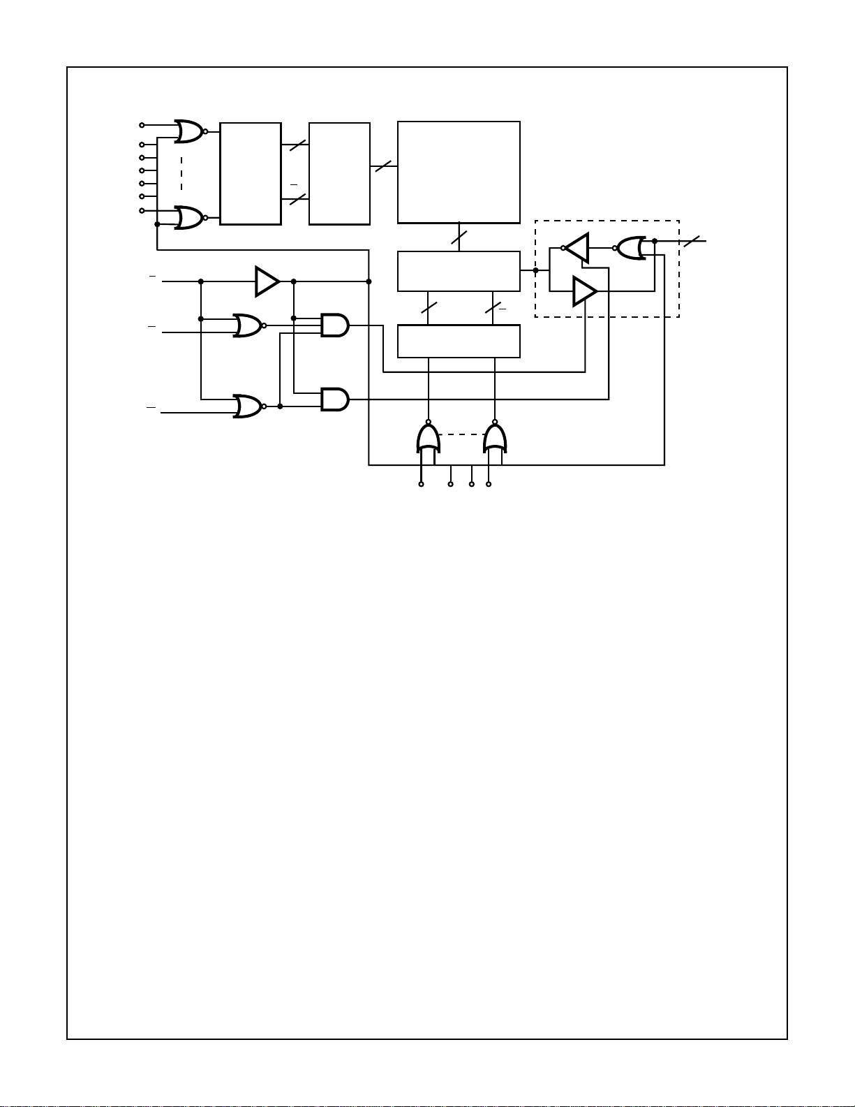
Functional Diagram
HM-65162
A1
A2
A3
A4
A5
A6
A7
A
ROW
ADDRESS
BUFFER
E
G
W
7
A
7
ROW
DECODER
128
MEMORY ARRAY
COLUMN DECODER
INPUT / OUTPUT (X8)
4
ADDRESS BUFFER
A0 A8 A9 A10
128 X 128
128
AND DATA
A
COLUMN
1 OF 8
DQ0
THRU
8
DQ7
4
A
6-2

HM-65162
Absolute Maximum Ratings Thermal Information
Supply Voltage . . . . . . . . . . . . . . . . . . . . . . . . . . . . . . . . . . . . .+7.0V
Input, Output or I/O Voltage . . . . . . . . . . . GND -0.3V to VCC +0.3V
Typical Derating Factor . . . . . . . . . . 05mA/MHz Increase in ICCOP
ESD Classification . . . . . . . . . . . . . . . . . . . . . . . . . . . . . . . . Class 1
Operating Conditions
Operating Voltage Range . . . . . . . . . . . . . . . . . . . . . +4.5V to +5.5V
Operating Temperature Range
HM-65162S-9, HM-65162B-9,
HM-65162-9, HM65162C-9. . . . . . . . . . . . . . . . . . -40oC to +85oC
CAUTION: Stresses abov e those listed in “Absolute Maximum Ratings” may cause permanent damage to the device. This is a stress only rating
and operation of the device at these or any other conditions above those indicated in the operational sections of this specification is not implied.
Thermal Resistance θJA(oC/W) θJC(oC/W)
CERDIP Package . . . . . . . . . . . . . . . . 48 8
CLCC Package . . . . . . . . . . . . . . . . . . 66 12
Maximum Storage Temperature Range . . . . . . . . .-65oC to +150oC
Maximum Junction Temperature. . . . . . . . . . . . . . . . . . . . . . +175oC
Maximum Lead Temperature (Soldering 10s). . . . . . . . . . . . +300oC
Die Characteristics
Gate Count . . . . . . . . . . . . . . . . . . . . . . . . . . . . . . . . . .26000 Gates
DC Electrical Specifications V
SYMBOL PARAMETER
ICCSB1 Standby Supply Current - 50 µA HM-65162B-9, IO = 0mA,
ICCSB Standby Supply Current - 8 mA E = 2.2V, IO = 0mA, VCC = 5.5V
ICCEN Enabled Supply Current - 70 mA E = 0.8V, IO = 0mA, VCC = 5.5V
ICCOP Operating Supply Current (Note 1) - 70 mA E = 0.8V, IO = 0mA, f = 1MHz,
ICCDR Data Retention Supply Current - 20 µA HM-65162B-9, IO = 0mA,
VCCDR Data Retention Supply Voltage 2.0 - V
II Input Leakage Current -1.0 +1.0 µA VI = VCC or GND, VCC = 5.5V
IIOZ Input/Output Leakage Current -1.0 +1.0 µA VIO = VCC or GND, VCC = 5.5V
V
IL
V
IH
VOL Output Low Voltage - 0.4 V IO = 4.0mA, VCC = 4.5V
VOH1 Output High Voltage 2.4 - V IO = -1.0mA, VCC = 4.5V
VOH2 Output High Voltage (Note 2) VCC -0.4 - V IO = -100µA, VCC = 4.5V
Input Low Voltage -0.3 0.8 V VCC = 4.5V
Input High Voltage 2.2 VCC +0.3 V VCC = 5.5V
= 5V ±10%; TA = -40oC to +85oC (HM-65162S-9, HM-65162B-9, HM-65162-9, HM-65162C-9)
CC
LIMITS
UNITS TEST CONDITIONSMIN MAX
E = VCC - 0.3V, VCC = 5.5V
- 100 µA HM-65162S-9, HM65162-9,
IO = 0mA, E = VCC - 0.3V,
VCC = 5.5V
- 900 µA HM-65162C-9, IO = 0mA,
E = VCC - 0.3V, VCC = 5.5V
VCC = 5.5V
VCC = 2.0V, E = VCC - 0.3V
-40µA HM-65162S-9, HM-65162-9,
IO = 0mA, VCC = 2.0V,
E = VCC - 0.3V
- 300 µA HM-65162C-9, IO = 0mA,
VCC = 2.0V, E = VCC - 0.3V
Capacitance T
SYMBOL PARAMETER MAX UNITS TEST CONDITIONS
CI Input Capacitance (Note 2) 10 pF f = 1MHz, All measurements are
CIO Input/Output Capacitance (Note 2) 12 pF
NOTES:
1. Typical derating 5mA/MHz increase in ICCOP.
2. Tested at initial design and after major design changes.
= +25oC
A
referenced to device GND
6-3
 Loading...