

HM-6516
March 1997
Features
• Low Power Standby. . . . . . . . . . . . . . . . . . . 275µW Max
• Low Power Operation . . . . . . . . . . . . . 55mW/MHz Max
• Fast Access Time. . . . . . . . . . . . . . . . . . 120/200ns Max
• Industry Standard Pinout
• Single Supply. . . . . . . . . . . . . . . . . . . . . . . . . . 5.0V V
• TTL Compatible
• Static Memory Cells
• High Output Drive
• On-Chip Address Latches
• Easy Microprocessor Interfacing
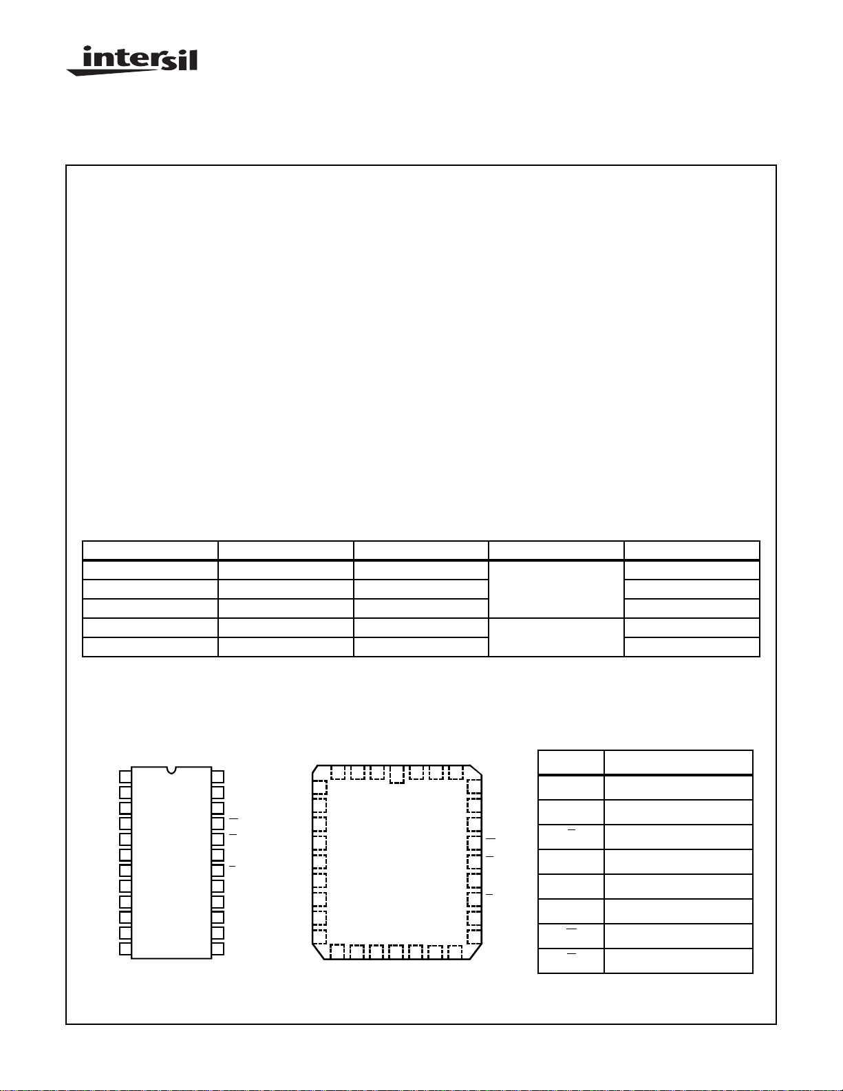
Ordering Information
2K x 8 CMOS RAM
Description
The HM-6516 is a CMOS 2048 x 8 Static Random Access
Memory. Extremely low power operation is achieved by the
use of complementary MOS design techniques. This low
power is further enhanced by the use of synchronous circuit
techniques that keep the active (operating) power low, which
also gives fast access times. The pinout of the HM-6516 is
the popular 24 pin, 8-bit wide JEDEC standard, which allows
CC
easy memory board layouts, flexible enough to accommodate a variety of PROMs, RAMS, EPROMs, and ROMs.
The HM-6516 is ideally suited for use in microprocessor
based systems. The byte wide organization simplifies the
memory array design, and keeps operating power down to a
minimum, because only one device is enabled at a time . The
address latches allow very simple interfacing to recent generation microprocessors which employ a multiplexed
address/data bus. The convenient output enable control also
simplifies multiplexed bus interfacing by allowing the data
outputs to be controlled independent of the chip enable.
120ns 200ns TEMP. RANGE PACKAGE PKG. NO.
HM1-6516B-9 HM1-6516-9 -40oC to +85oC CERDIP F24.6
- 29102BJA -55oC to +125oC JAN# F24.6
8403607JA 8403601JA -55oC to +125oC SMD# F24.6
- HM4-6516-9 -40oC to +85oC CLCC J32.A
8403607ZA 8403601ZA -55oC to +125oC SMD# J32.A
Pinouts
A7
A6
A5
A4
A3
A2
A1
A0
DQ0
DQ1
DQ2
GND
1
2
3
4
5
6
7
8
9
10
11
12
HM-6516
(CERDIP)
TOP VIEW
24
V
CC
23
A8
22
A9
21
W
20
G
19
A10
18
E
17
DQ7
16
DQ6
15
DQ5
14
DQ4
13
DQ3
A6
A5
A4
A3
A2
A1
A0
NC
DQ0
5
6
7
8
9
10
11
12
13
14
HM-6516
(CLCC)
TOP VIEW
CC
V
NC
NC
A7
NC
1
3 2
4 32 31 30
16 17 18 19 20
15
DQ1
DQ2
GND
NC
DQ3
NC
DQ4
NC
DQ5
PIN DESCRIPTION
29
A8
28
A9
27
NC
26
W
G
25
A10
24
E
23
22
DQ7
DQ6
21
NC No Connect
A0 - A10 Address Inputs
E Chip Enable/Power Down
VSS/GND Ground
DQ0 - DQ7 Data In/Data Out
V
CC
Power (+5V)
W Write Enable
G Output Enable
CAUTION: These devices are sensitive to electrostatic discharge; follow proper IC Handling Procedures.
http://www.intersil.com or 407-727-9207
| Copyright © Intersil Corporation 1999
6-1
File Number 2998.1
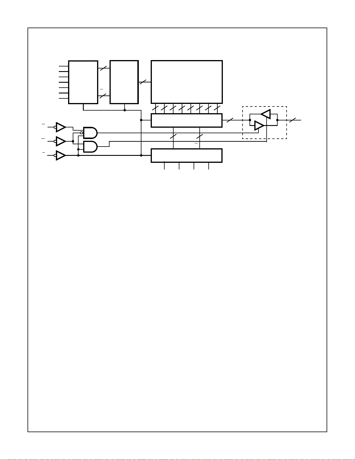
Functional Diagram
HM-6516
A10
A9
A8
A7
A6
A5
A4
G
W
E
LATCHED
ADDRESS
REGISTER
A
7
GATED
ROW
DECODER
A
7
LG
128
16
G
L
A3 A2 A1 A0
128 x 128
MATRIX
16
16
16
16
GATED COLUMN
DECODER
44
A
LATCHED ADDRESS
REGISTER
16 16
A
1 OF 8
16
A
8
A
DQ0
THRU
8
DQ7
6-2
 Loading...