

Intersil Corporation HIP9022 Datasheet
HIP9022
PRELIMINARY
Data Sheet October 1998 File Number 4509.1
Dual High Speed Laser Driver
The HIP9022 Dual High Speed Laser Driver is designed to
operate with a constant current drain from the power supply.
This current defines the laser operating power . The current is
accurately controlled in the range of 0.5A to 2A to deliver
constant optical power from the laser when used with an
external Pow erFETandPower Sense resistor. The operating
circuit allows flexibility in choosing driver current le vels.
Eight S/H circuits are multiplex bus controlled to provide
analog data for the dual laser drivers. The bus is updated
during the blanking period of the laser printer scan with a
data rate up to 2.5MHz. A “thermo-electric-cooler” control
circuit provides temperature control of the laser. Two on-chip
ESD diodes protect each laser.
A principle advantageof the Dual High Speed Laser Driver is
accomplished by managing the high currents externally with
discrete PowerFETs and thereby not forcing large switching
currents to exist on the same IC substrate with the precision
control circuitry.
Ordering Information
TEMP.
PART NUMBER
HIP9022AM
RANGE (oC) PACKAGE PKG. NO.
0 to 100
68 Ld PLCC N68.95
Features
• Dual High Speed Laser Driver with Data Rates up to
2.5MHz
• 0.5A to 2A Range of Constant Current Source Controlled
to 0.1% Full Scale
• Low Signal Transients with Controlled Constant Current
Switching
• Laser Optical Power Controlled to Better than 0.5%
• Thermoelectric Cooler (TEC) Circuit to Control
Temperature to within 0.25
o
C
• Multiplexed Sample/Hold (S/H) Bus Interface
• Serial Diagnostic Bus with Multiplexed Output
• High Current ESD Diodes for Laser Diode Protection
Applications
• Dual Laser Printer Driver
Pinout
VUP1
SG_1
VLOW1
V
GNDA1
GNDD1
CC1
XTEN1+
XTEN1CTC1-10K
CTC1-27K
LASERON1B
OC1
TECFB1
TECREF1
TECGDR1
TRES1
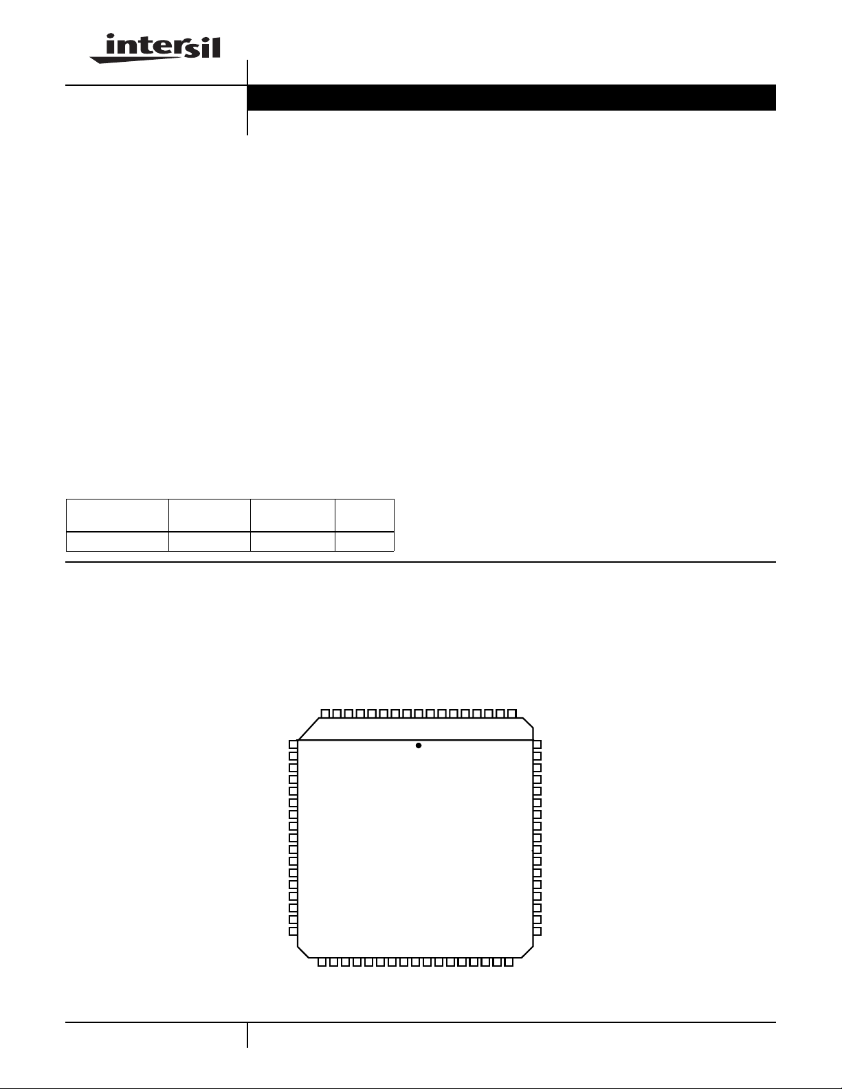
HIP9022 (PLCC)
TOP VIEW
ESD LASER GND
ESD LASER GND
ESD SHUNT DRAIN-1
ESD SHUNT DRAIN-1
ESD SHUNT DRAIN-1
ESD LASER PS-1
ESD LASER PS-1
VDDNC
10
11
12
13
EE
14
15
16
17
18
19
20
21
22
23
24
25
26
27 28 29 30 31 32 33
NC
OT1
INVERT
RESETB
DIAGINB
NULLB
ESD SHUNT DRAIN-2
123456789
68 67 66 65 64 63 62 61
34
IN
A3
CC
NC
V
V
SB_H
ESD SHUNT DRAIN-2
ESD SHUNT DRAIN-2
ESD LASER PS-2
ESD LASER PS-2
RLY_IN
RLY_OUT
V9P
434241403938373635
A0
A1
A2
DIAG
NC
TECREFR
60
59
58
57
56
55
54
53
52
51
50
49
48
47
46
45
44
VUP2
SG_2
VLOW2
GNDA2
GNDD2
CC2
XTEN2+
XTEN2CTC2-10K
CTC2-27K
LASERON2B
OC2
TECFB2
TECREF2
TECGDR2
TRES2
OT2
4-1
CAUTION: These devices are sensitive to electrostatic discharge; follow proper IC Handling Procedures.
http://www.intersil.com or 407-727-9207
| Copyright © Intersil Corporation 1999

X
HIP9022
+12V
1µF
NC
VUP1
SG_1
VLOW1
-5V
1µF
V
EE
GNDA1
GNDD1
CC1
XTEN1+
XTEN1-
CTC2-10K
CTC1-27K
LASER_ON1B
OC1
TECFB1
TECREF1
TECGDR1
TRES1
OT1
NC
INVERT
ESD
LASERPS-1
7
8
V
V
DD
DD
9
10
11
12
13
14
15
16
17
18
19
20
21
PU
22
23
24
25
26
27
28
29 30 31 32 33
RESETB
DIAGINB
SHUNT
DRAIN-1
56
9V REG.
V/I REF.
LASER DRIVER-1
PUPU PUPDPD
NULLB
ESD
4
V9P
SB_H
3
LD1
34
NC
ESD
LASER
GNDGND
12
SAMPLE/HOLD
SYSTEM
35 37 38 39 40
V
IN
ESD
SHUNT
DRAIN-2
68
LD2
36
V
A3 A2 A1 A0
CC
+5V
LASERPS-2
6667
ESDD2ESDD1
LASER
GATE
DRIVE
A5
12kΩ
30kΩ
PU PU PU PU
ESD
65
64
A4
+
-
OTA GATE
DRIVE AMP.
+
-
A2
CURRENT
MONITOR
1kΩ
AMP.
A1
ON/OFF
O. C.
COMP.
TEC DRIVER
(THERMO
ELECTRIC
COOLER
CIRCUIT)
AND
OVER/UNDER
TEMPERATURE
COMPARATOR
LASER DRIVER-2
V
TEST
OUT
DIAG
A3
+
-
11kΩ
11kΩ
V
CC
+
-
X10
THERM.
COMP
+
-
+
-
41 42
A6
PU
1.9V
NC
63
RLY_IN
PD
62
RLY_OUT
V9P
61
60
VUP2
59
SG_2
58
VLOW2
57
GNDA2
56
GNDD2
55
CC2
54
XTEN2+
53
XTEN2-
52
CTC2-10K
51
CTC2-27K
50
LASER_ON2B
49
OC2
48
TECFB2
47
TECREF2
46
TECGDR2
45
TRES2
44
OT2
NOTE:
PU = 60kΩ PULLUP RESISTOR
PD = 60kΩ PULLDOWN RESISTOR
= SCHMITT TRIGGER HYSTERESIS
43
TECREFR
(TEMP. REF.
RESISTOR)
5 - 10kΩ
V
CC
+9V
1µF
1µF
1µF
0.1µF
0.1µF
(THERMO-RESISTOR
SENSES LASER TEMP.,
NEG. TEMP. COEF.,
TEC COOLS LASER.)
TO V
CC
TO GND
LASER P.S.
3 TO 5V
Q3
RF3V49092
Q2
0.02µF
RFD3055
OR
EQUIV.
RELAY1
LASER
I
DL
R
S
0.25Ω
TEC P.S.
3V
Q1
TEC
X
THERMAL RELATED COMPONENTS
FIGURE 1. HIGH SPEED LASER DRIVER FUNCTIONAL BLOCK DIAGRAM SHOWN IN QUIESCENT P.S. CURRENT TEST MODE
4-2

HIP9022
Pin Descriptions
PIN
NUMBER SYMBOL DESCRIPTION
1, 2 ESD LASER GND Laser supply and system ground.
3, 4, 5 ESD SHUNT DRAIN-1 Laser diode ESD protection.
6, 7 SD LASER PS-1 Laser power supply ESD protection.
8VDDInput for 12V power supply.
9 NC No connection.
10 VUP1 Filter capacitor for internally generated shunt gate upper voltage level (1µF).
11 SG_1 Drive output to shunt Power FET gate.
12 VLOW1 Filter capacitor for internally generated shunt Power FET gate lower drive voltage level (1µF).
13 V
14 GNDA1 Analog Ground.
15 GNDD1 Digital Ground.
16 CC1 Gate drive to the current source Power FET.
17 XTEN1+ Times 10 constant current monitor amplifier input from the high side of the sense resistor.
18 XTEN1- Times 10 constant current monitor amplifier input from the low side of the sense resistor.
19 CTC1-10K Thermal compensation short time constant where TTC= External C x 10kΩ. (External C typically equal
20 CTC1-27K Thermal compensation long time constant where TTC= External C x 27kΩ. (External C typically equal
21 LASERON1B Input control turns shunt Power FET gate drive ON/OFF with 5V CMOS logic. Low turns the shunt Power
22 OC1 Laser over-current indicator flag.
23 TECFB1 Feedback to stabilize the TEC loop.
24 TECREF1 Feedback to stabilize the TEC loop.
25 TECGDR1 Thermo-Electric Cooler Power FET gate drive.
26 TRES1 Thermo-Resistor output to ground connection for TEC control.
27 OT1 Laser out of temperature range indication.
28 NC No connection.
29 INVERT High input converts to operation with Pmos Current source and NDmos shunt Power FET external
30 RESETB WhenRESETB is held low,three reset actions occur. The LASERONB input is defeated to a Laser Off con-
31 DIAGINB Low level activates the diagnostic mode. This pin has an internal pull-up.
32 NULLB Auto-zeros the S/H amplifier selected by address when held low. This pin has an internal pull-up.
33 SB_H Samplesthe selected address when held low.The setup time for address is <25ns. This pin has an internal
34 NC No connection.
35 V
36 V
37 A3 Refer to the Table 1 Address Map. The A3 - A0 pins have an internal pull-up.
EE
IN
CC
Input for -5V power supply.
0.02µF).
0.1µF).
FET OFF and the Laser ON. These pins have an internal pull-up.
transistors. Low input converts to operation with NDmos Current source and Pmos high side shunt Power
FET external transistors. This pin has an internal pull-down.
dition. The SG_1, 2 outputs are switched to VLOW when in the INVERT low mode and to VUP when in the
INVERT high mode. The TEC amplifier is turned off to switch the TECGDR1, 2 outputs to Ground. This pin
has an internal pull-down.
pull-up.
Analog voltage sampled by selected S/H. The input voltage range is 0 to 5V. There is an internal voltage
clamp for voltage outside of this range. There is an internal 2 - 3µs filter for noise rejection.
Input for 5V power supply.
4-3
 Loading...