


HIP9021
PRELIMINARY
August 1996
Features
• MOSFET Driver and DC Motor Controller
• Torque Control and Overload Protection
• Battery Power Supply . . . . . . . . . . . . . . . . +5V to +15V
• BiMOS IC with Low Operating Current
- Maximum Supply Current . . . . . . . . . . . . . . . . .1.5mA
- Maximum Input Leakage Currents . . . . . . . . . . 1.5µA
• 500µA Maximum Supply Current
•1µA Maximum Input Leakage Currents
• Typical Oscillator Frequency . . . . . . . . . . . . . . . . .5kHz
• Power-On-Reset Control
• 10mA Drive Capability for Gate Output
• Operating Temperature. . . . . . . -40
o
Applications
• Portable Battery Operated Electric Drills
• Controller for Small DC Electric Motors
• Torque/Drive Controller for Inductive Loads
• Intelligent MOSFET Drive
Ordering Information
TEMP.
PART NUMBER
HIP9021IB -40 to +85 8 Ld SOIC M8.15
RANGE (oC) PACKAGE
N-Channel MOSFETs in Motor Control Systems
C to +85oC Range
Portable Battery Drive/Torque Controller for
Description
The HIP9021IB is a dedicated Power MOSFET driver which
drives a DC motor. As a system, motor speed is controlled
while controlling torque. The primary application is drive control for portable drills while providing overload protection.
The main function of the HIP9021IB is to produce a pulse
width modulated square wave signal which drives the gate of
an N-Channel Power MOSFET. The duty-cycle is determined by the setting of an external potentiometer at the
TRIGGER (speed control) input. As the TRIGGER voltage
level is decreased the duty-cycle of the square wave and the
speed of the motor is increased.
The torque of the motor is limited by the voltage level sensed
at the drain of the external Power MOSFET. When the current reaches an adjustable limit set at the TORQUE input,
the drive of the Power MOSFET is disabled.
The system control components include 2 adjustable potentiometer controls and 2 capacitors for the operating frequency and torque delay control. A fixed or battery supply
voltage in the range of 5V to 15V may be used.
The HIP9021IB is provided in a small outline plastic package
for a compact surface mount to a ceramic substrate. The
surface mount assembly can be fit directly into the trigger of
a portable electric drill.
PKG.
NO.
Pinout
HIP9021IB
(SOIC)
TOP VIEW
DRAIN
1
GND
OSC
2
3
4
TRIGGER
CAUTION: These devices are sensitive to electrostatic discharge; follow proper IC Handling Procedures.
http://www.intersil.com or 407-727-9207
| Copyright © Intersil Corporation 1999
8
V
DD
7
GATE
6
DELAY
5
TORQUE
1
File Number 4055
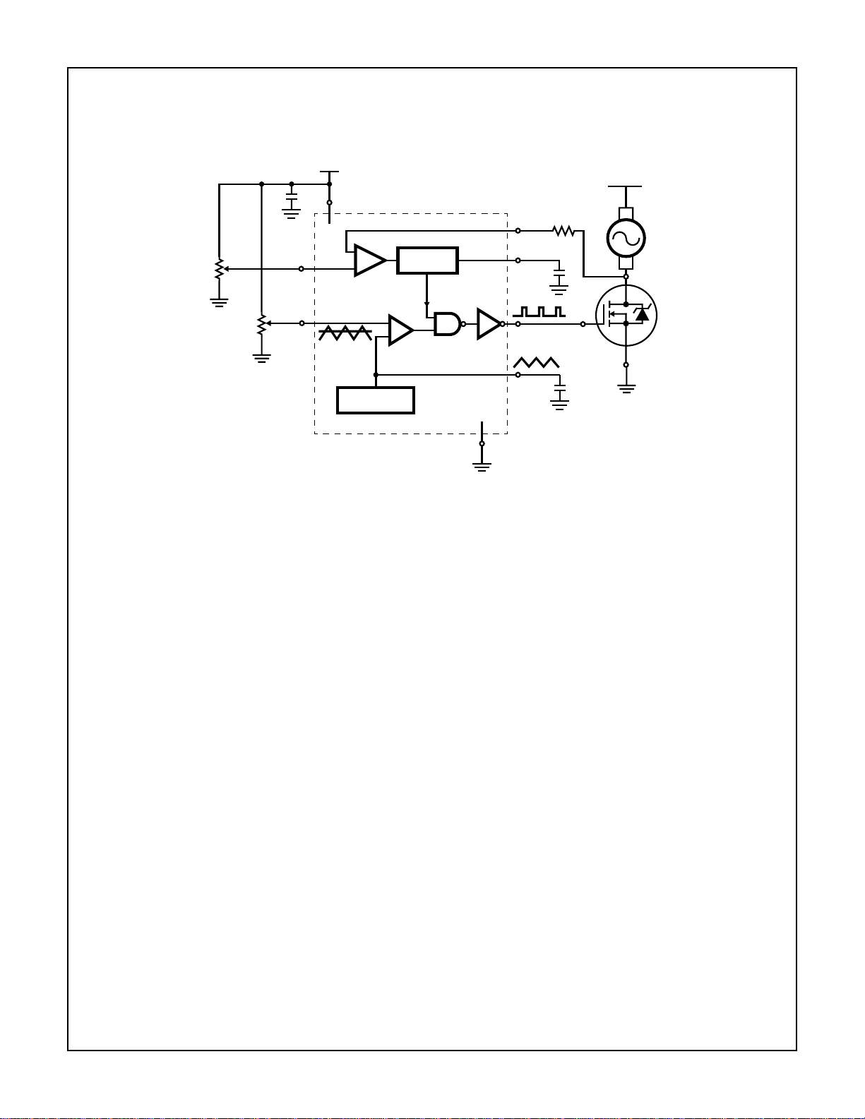
Block Diagram
HIP9021
V
BATT
V
DD
+
DRAIN
TORQUE
LEVEL SET
TORQUE
TRIGGER
SPEED
CONTROL
+
-
OSCILLATOR
HIP9021
CONTROL
& LOGIC
GC
+
DELAY
GATE
OSC
GND
2

HIP9021
Absolute Maximum Ratings Thermal Information
Supply Voltage . . . . . . . . . . . . . . . . . . . . . . . . . . . . . . . . . . . . . +16V
Input Voltage. . . . . . . . . . . . . . . . . . . . . . . GND -0.3V to VCC +0.3V
Maximum Current, IDD. . . . . . . . . . . . . . . . . . . . . . . . . . . . . . .50mA
Maximum Transient Reverse Current, IR (10s). . . . . . . . . . . . -50mA
Operating Conditions
Typical Power Supply Voltage. . . . . . . . . . . . . . . . . . . . . . . . . . .7.5V
Operating Voltage Range . . . . . . . . . . . . . . . . . . . . . . . +5V to +15V
Operating Temperature Range. . . . . . . . . . . . . . . . . -40oC to 150oC
Typical Oscillator Frequency. . . . . . . . . . . . . . . . . . . . . . . . . . . 5kHz
CAUTION: Stresses above those listed in “Absolute Maximum Ratings” may cause permanent damage to the device. This is a stress only rating and operation
of the device at these or any other conditions above those indicated in the operational sections of this specification is not implied.
Thermal Resistance (Typical, Note 1) θJA (oC/W)
SOIC Package. . . . . . . . . . . . . . . . . . . . . . . . . . . . . 175
Maximum Storage Temperature Range . . . . . . . . . .-65oC to 150oC
Maximum Junction Temperature . . . . . . . . . . . . . . . . . . . . . . 150oC
Maximum Lead Temperature (Soldering 10s). . . . . . . . . . . . . 300oC
(Lead Tips Only)
Electrical Specifications V
DD
PARAMETER SYMBOL TEST CONDITIONS MIN TYP MAX UNITS
DC Supply Current I
OSC Source Current +I
OSC Sink Current -I
OSC Threshold Voltage V
OSC Trigger Voltage V
TRIGGER Input Leak Current I
TORQUE Input Leak Current I
DELAY Current at 1V I
DELAY Current at 2V I
DELAY Threshold Voltage V
DRAIN Input Resistance R
DRAIN Current I
GATE Output Source Current I
GATE Output Voltage V
GATE Output Slew Rate V
= 7.5V, Figure 1 Test Circuit, Table 1 Conditions, TA = +25oC Unless Otherwise Specified
DD
OSC
OSC
OSC(TH)
OSC(TR)
TRIGGER
TORQUE
DELAY1
DELAY2
DELAY(TH)
DRAIN
DRAIN
GATE
GATE
GATE(S/R)
Measured in Typical Application Circuit,
Duty Cycle = 50%, See Figure 2
0.1 1.2 3.1 mA
19 25 32 µA
-32 -25 -19 µA
4.75 4.95 5.25 V
2.30 2.45 2.65 V
- 0.02 1.5 µA
- 0.02 1.5 µA
1.5 3.4 6 µA
13250 mA
1.8 1.9 2 V
150 260 350 kΩ
1 1.7 4.6 mA
10 18 - mA
6.5 7.4 - V
-10- V/µs
DELAY Output Framed Pulse
Duty Cycle
FP/DC Gate Duty Cycle = 50%;
V
TORQUE
= GND; V
DRAIN
= V
GATE;
DELAY =10kΩ to GND, Ref er to Figure 1
DELAY Output Framed Pulse Delay, V
GATE
to V
DELAY
Typical Oscillator Frequency f
FP/DLY
OSC
for the Test circuit and Timing Diagram of
the DELAY Output Pulse Frame.
TA = 25oC - 5 - kHz
TA = -40oC - 7.2 - kHz
TA = 85oC - 3.6 - kHz
NOTES:
1. θJA is measured with the component mounted on an evaluation PC board in free air.
3
-44- %
-3- %
2V
5V
7.5V
15KΩ
1V
2V
5V
2V
5V
V
TRIGGER
22nF
V
DRAIN
1nF
V
TORQUE
1nF
1
DRAIN
5
TORQUE
2
TRIGGER
V
DD
OSC
HIP9021
V
DD
CONTROL
+
-
+
HIP9021
10µF
8
+
& LOGIC
GC
GND
0.01µF
10nF
1nF
1V
2V
3.75V
2.5V
5V
10K
R
D
V
DELAY
6
DELAY
V
V
GATE
OSC
7
GATE
4
OSC
3
V
GATE
V
DELAY
GATE PULSE WIDTH
FRAMED PULSE WIDTH
FRAMED PULSE DELAY
V
DD
GND
1V
GND
NOTE: The timing diagrams relate to the delay output framed pulse and show the time duration of the delay pulse “framed” inside of the gate
pulse. The framed pulse duty cycle and delay, in percent, are measured in reference to the gate pulse which is set at 50% duty cycle. The
Delay output framed pulse delay is one-half of the difference of the gate pulse width minus delay output framed pulse width.
FIGURE 1. ELECTRICAL CHARACTERISTICS TEST CIRCUIT FOR SIGNAL FUNCTIONS OF THE HIP9021
TABLE 1. SWITCH POSITIONS OF FIGURE 1 FOR ELECTRICAL CHARACTERISTIC TESTING
SYMBOL DRAIN TRIGGER OSC TORQUE DELAY GATE MEASURE
I
DD
+I
OSC
-I
OSC
V
OSC(TH)
V
OSC(TG)
I
TRIGGER
I
TORQUE
I
DELAY1
I
DELAY2
V
DELAY(TH)
R
DRAIN
I
DRAIN
V
GATE
I
GATE
V
GATE(S/R)
15KΩ to 2V GND 3.75V 2V Open Open IDD Current Into VDDPin
15KΩ to 2V GND 2.5V 2V Open Open Source Current From OSC Pin
15KΩ to 2V GND 5V 2V Open Open Sink Current Into OSC Pin
1V Open 1nF 2V Open Open Positive Peak OSC Voltage
1V Open 1nF 2V Open Open Negative Peak OSC Voltage
15KΩ to 2V 5V 5V 2V Open Open TRIGGER Leakage Current
15KΩ to 2V Open 5V 5V Open Open TORQUE Leakage Current
15KΩ to 2V 7.5V 1nF Open 1V Open Current to DELAY Pin
15KΩ to 2V 7.5V 1nF Open 2V Open Current to DELAY Pin
1V Ramp Up 1nF 2V GND Read V
GATE
Measure V
V
Less Than 0.5V
GATE
TRIGGER
When
5V GND 1nF 2V GND Open DRAIN Current; Calculate
R
= 5V/I
DRAIN
DRAIN
1V 7.5V 5V 2V Open Open DRAIN Current
5V GND 1nF 2V Open Open Measure V
2V GND 1nF 2V GND Set to
V
-0.5V
OUT
Measure I
with V
GATE
= V
GATE
Source Current
GATE
= V
OUT
OUT
-0.5V
Refer to Figure 2 Application Circuit, 50% GATE Output Duty Cycle GATE Output Slew Rate
FP/DC Reference Figure 1 Waveforms
FP/DLY Reference Figure 1 Waveforms
f
OSC
1V V
OSC(TH)
-
1nF 2V GND 25KΩ Load GATE Output Timing
-1V
4
HIP9021
Pin Descriptions
NAME NUMBER DESCRIPTION
DRAIN 1 The input to the DRAIN pin senses the drain of a power MOSFET Output Motor Driver. The DRAIN volt-
age is an image of the current flowing through the power MOSFET. By limiting this voltage, the torque of
the motor can be controlled.
TRIGGER 2 The TRIGGER input is an analog voltage control level used to fix the duty-cycle at the DRAIN Output. A
voltage level here is determined by a potentiometer adjustment. The TRIGGER voltage level is com-
pared with the triangle signal from the internal oscillator to produce a pulse-width modulated signal.
GND 3 Negative pole of the battery or system ground reference.
OSC 4 Oscillator output normally terminated in a charge/discharge capacitor. A constant current is flowing in
and out to charge and discharge the external capacitor.
TORQUE 5 The TORQUE input is a reference level adjustment for torque control. The voltage reference is compared
with DRAIN input. If V
DELAY 6 An external capacitor at the DELAY output is used to delay the torque control action. The external ca-
pacitor at the DELAY pin will start to be charged if a MOSFET output over-current condition is detected.
The purpose of the capacitor is to delay the disabling action of the signal GATE drive.
GATE 7 The GATE output drives the Gate of the Power MOSFET.
DRAIN
> V
TORQUE
, the GATE output pulse drive must be disabled.
V
DD
7.5V 330Ω
180K
TORQUE
LEVEL SET
100K
5.6K
8 Positive pole of the battery or Power Supply Voltage, nominally 7.5V.
SW
V
1µF
200K
270K
CONTROL
TORQUE
470K
TRIGGER
1nF
SPEED
DD
+
OSCILLATOR
HIP9021
+
-
CONTROL
& LOGIC
GC
+
GND
DRAIN
DELAY
GATE
OSC
15K
3.3µF
1nF
V
BATT
PORTABLE
ELECTRIC
DRILL MOTOR
RFP45N03L
N-CHANNEL
POWER
MOSFET
NOTE: The value chosen for the torque level set pot is dependent on the type of power MOSFET and motor characteristics.
The TRIGGER is a combined SW/Speed Control function. Motor speed increases as the TRIGGER voltage decreases.
Speed control range: 2.35V (Min) < V
TRIGGER
< 5.25V (Max)
FIGURE 2. TYPICAL OPERATING CIRCUIT SHOWING THE HIP9021IB AS AN N-CHANNEL MOSFET DRIVER IN A PORTABLE
BATTERY ELECTRIC DRILL APPLICATION
5
HIP9021
Functional Description
Oscillator
The Oscillator triangle waveform is generated by the charge
and discharge of a 1nF external capacitor connected to the
OSC pin. The OSC terminal has a source and sink drive from a
current mirror which delivers ±25µA. The charge and discharge
of the external capacitor is controlled by 2 comparators which
compare respectively V
V
. The period of the triangle wave is nominally 200µs.
DD
Gate Driver
The TRIGGER input signal is compared from the triangle
waveform of the oscillator to produce a square wave signal.
The duty cycle of the GATE dr ive signal is increased as the
TRIGGER input level increases. The output of the comparator is then NANDed with a GATE Control signal which can
enable or disable the GATE output. The NAND gate output is
buffered to deliver 18mA typical GATE drive current.
Torque Effect
The triangle signal, after going through a divider, is also
compared with TRIGGER input level. This produces another
square wave of the same period but with a duty-cycle that is
smaller than the GATE by ~5%. This square wave is used to
enable the comparison between DRAIN and TORQUE
inputs while the MOSFET is conducting.
with 2/3 VDD and V
OSC
OSC
with 1/3
A torque effect condition exists when 80% of the DRAIN signal is higher than the TORQUE input level set voltage of the
potentiometer. During this time, the e xternal delay capacitor of
3.3µF is charged through an internal 100K resistor. When the
voltage at the DELAY pin reaches 0.25 x V
, the RS flip-flop
DD
is then set and the Gate Control (GC) signal shown in Figure
3 goes to low. The Output GATE drive signal is then disabled.
This situation remains even if the voltage on the DELAY pin
stays under 0.25 x V
for a sustained period of time.
DD
At the same time, when the RS flip-flop is set, the external
capacitor at the DELAY pin is discharged via the nMOS
device, Q2 which is driven by the Q output of the flip-flop.
Power-On Reset (POR)
In reference to Figure 3, the power on of the chip will cause
the reset of the RS Gate Control flip-flop when Q1 is
switched low. As an initial condition, the Gate Control (GC)
signal is reset high. Since power on is the only way to reset
the RS flip-flop, a disabled GATE drive signal due to a torque
effect condition requires a switched (trigger) reset.
The POR (power on reset) threshold requires that V
DD
be less
than 2V to initiate a reset. The POR circuit is based on the
behavior of the voltage reference cell that produces a constant
1.15V (REF. BIAS) when V
is over 2V. When Q1 is forward
DD
biased, the Q1 drain voltage goes low to reset the input of the
RS flip-flop.
TORQUE
TRIGGER
1nF
OSC
PULL
DOWN
OSC
V
DD
-
φ
50K
φ
200K
6K
2K
2K
40K
+
LOAD
COMP
REF.
BIAS
1.15V
Q1
+
DELAY
COMP
+
-
+
150K
POR
φ
100K
φ
330K
R
S
Q
Q
CONTROL
Q2
GATE
(GC)
BUF
DELAY
DRAIN
GATE
3.3µF
15K
V
BATT
MOTOR
POWER
MOSFET
φ
φ
FIGURE 3. DETAILED LOGIC DIAGRAM OF THE PORT ABLE DRIVE/T ORQUE CONTROLLER FOR N-CHANNEL POWER MOSFETS
SHOWING THE DRAIN AND T ORQUE, THE GATE CONTROL LOGIC AND THE TRIGGER (SPEED) CONTROL.
6
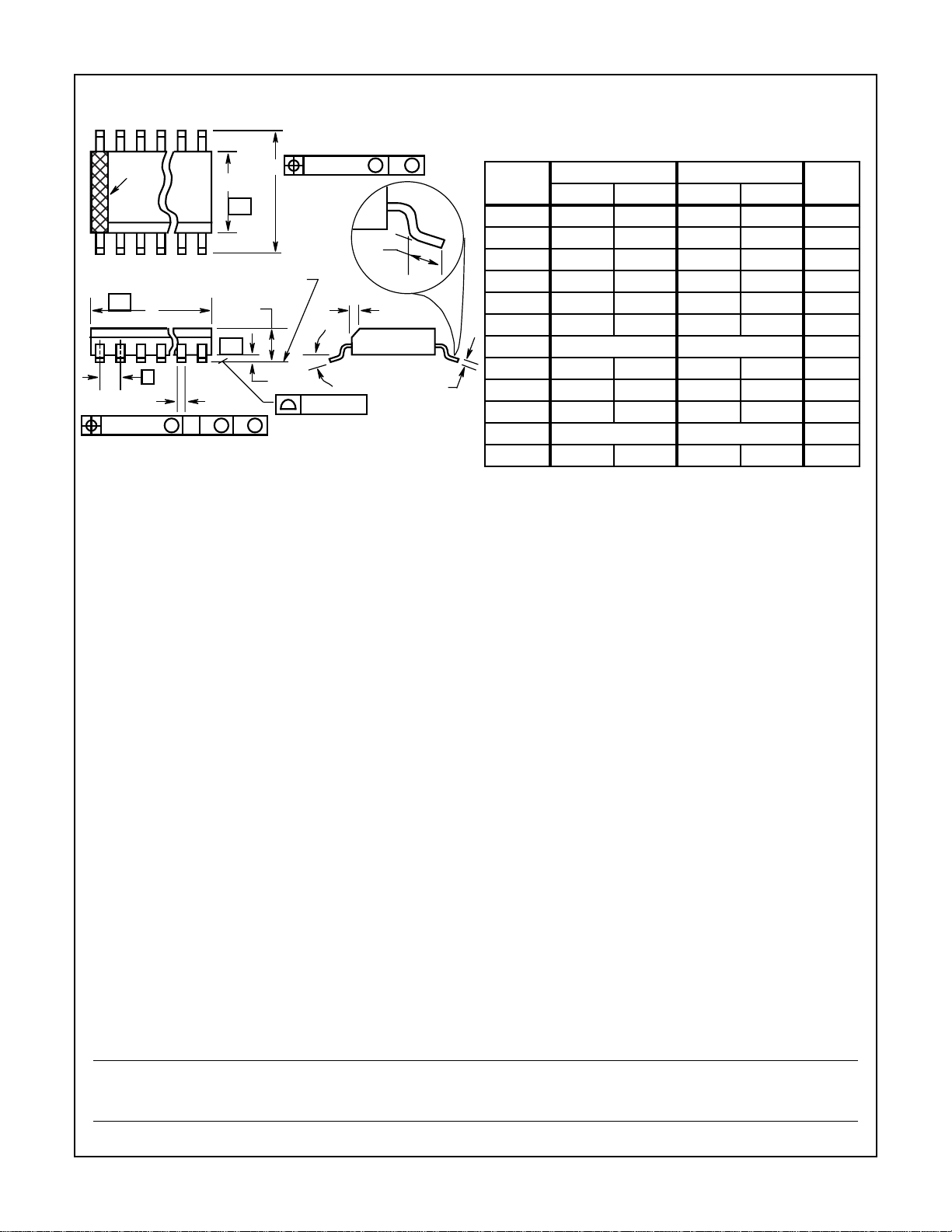
Small Outline Plastic Packages (SOIC)
HIP9021
N
INDEX
AREA
123
-A-
0.25(0.010) B
H
E
-B-
SEATING PLANE
D
A
-C-
M
L
h x 45
M
o
α
e
B
0.25(0.010) C AMB
M
NOTES:
1. Symbols are defined in the “MO Series Symbol List” in Section
2.2 of Publication Number 95.
2. Dimensioning and tolerancing per ANSI Y14.5M-1982.
3. Dimension “D” does not include mold flash, protrusions or gate
burrs. Mold flash, protrusion and gate burrs shall not exceed
0.15mm (0.006 inch) per side.
4. Dimension “E” does not include interlead flash or protrusions. Interlead flash and protrusions shall not exceed 0.25mm (0.010
inch) per side.
5. The chamfer on the body is optional. If it is not present, a visual
index feature must be located within the crosshatched area.
6. “L” is the length of terminal for soldering to a substrate.
7. “N” is the number of terminal positions.
8. Terminal numbers are shown for reference only.
9. The lead width “B”, as measured 0.36mm (0.014 inch) or greater
above the seating plane, shall not exceed a maximum value of
0.61mm (0.024 inch).
10. Controlling dimension: MILLIMETER. Converted inch dimensions are not necessarily exact.
A1
0.10(0.004)
S
M8.15 (JEDEC MS-012-AA ISSUE C)
8 LEAD NARROW BODY SMALL OUTLINE PLASTIC PACKAGE
INCHES MILLIMETERS
SYMBOL
A 0.0532 0.0688 1.35 1.75 -
A1 0.0040 0.0098 0.10 0.25 -
B 0.013 0.020 0.33 0.51 9
C 0.0075 0.0098 0.19 0.25 D 0.1890 0.1968 4.80 5.00 3
E 0.1497 0.1574 3.80 4.00 4
e 0.050 BSC 1.27 BSC H 0.2284 0.2440 5.80 6.20 -
C
h 0.0099 0.0196 0.25 0.50 5
L 0.016 0.050 0.40 1.27 6
N8 87
o
α
0
o
8
o
0
o
8
Rev. 0 12/93
NOTESMIN MAX MIN MAX
-
All Intersil semiconductor products are manufactured, assembled and tested under ISO9000 quality systems certification.
Intersil products are sold by description only. Intersil Corporation reserves the right to make changes in circuit design and/or specifications at any time without
notice. Accordingly, the reader is cautioned to verify that data sheets are current before placing orders. Information furnished by Intersil is believed to be accurate
and reliable. However, no responsibility is assumed by Intersil or its subsidiaries f or its use; nor for any infringements of patents or other rights of third parties which
may result from its use. No license is granted by implication or otherwise under an y patent or patent rights of Intersil or its subsidiaries.
For information regarding Intersil Corporation and its products, see web site http://www.intersil.com
7
 Loading...