

HIP7030A0
PRELIMINARY
April 1994
Features
• HIP7030A2 Microcontroller Emulation
- All HIP7030A2 Hardware and Software Features
- Timing and Performance Equivalent to HIP7030A2
• On-Chip Memory
- 176 Bytes of RAM - No ROM
• Full 8K Byte Address Space Available Externally
• Non-Multiplexed External Address and Data Lines
- I/O Memory Interface Matches Industry Standard
EPROM/EEPROMS for True Emulation with Two
Chips
• FS Line Identifies Fetch Cycles for Breakpoint Logic
o
C to +125oC Operating Range
• -40
• Single 3.0V to 6.0V Supply
• Available in 68 Lead PLCC Packages
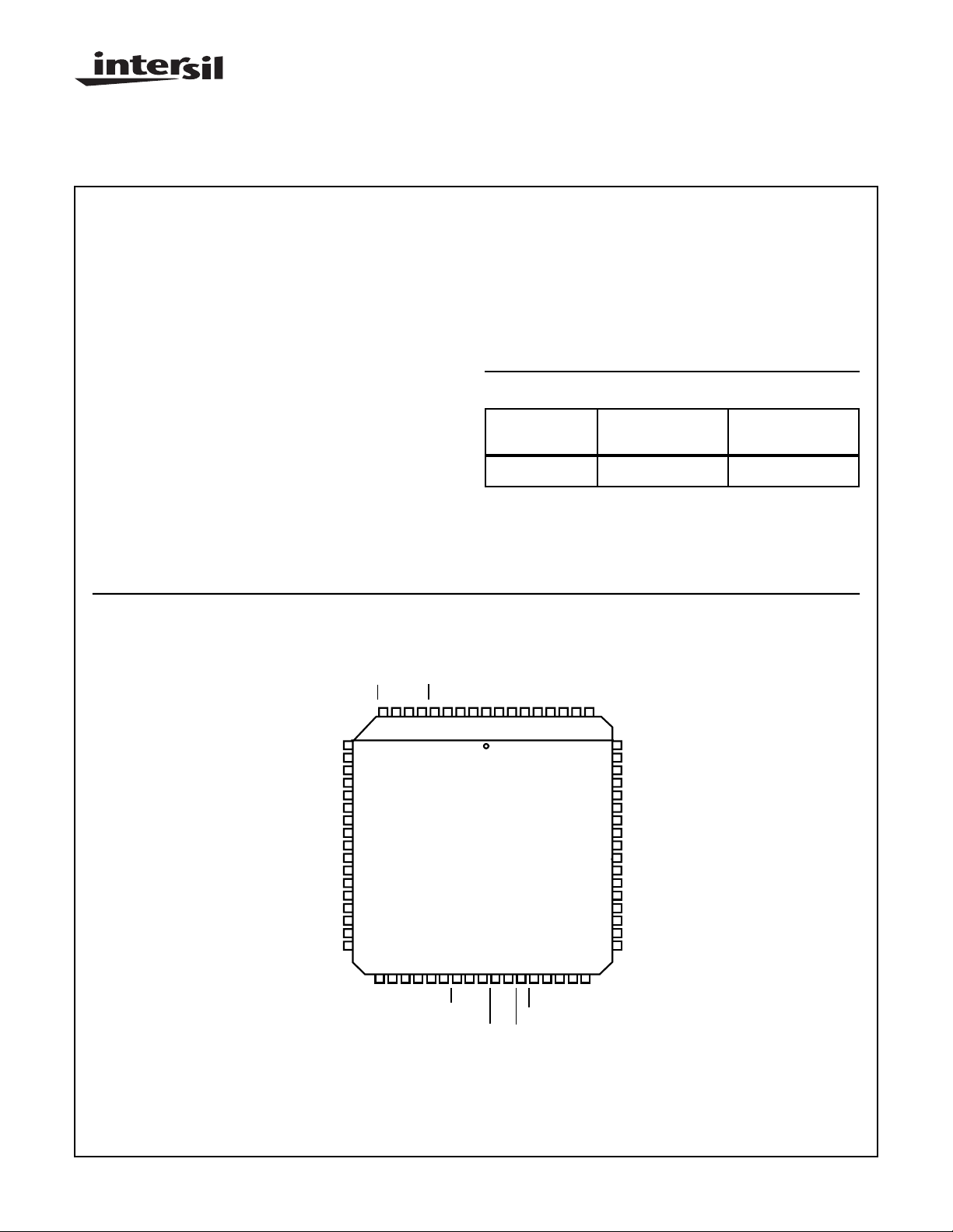
J1850 8-Bit 68HC05 Microcontroller
Emulator Version
Description
The HIP7030A0 Emulator is functionally equivalent to the
HIP7030A2 microcontroller with the addition of external data
bus, address bus, and control signals which provide off chip
address capability. It is designed to permit prototype and
pre-production development of systems for mask programmed applications. The HIP7030A0 is also intended for
construction of development systems for the HIP7030A2.
Ordering Information
TEMPERATURE
PART NUMBER
HIP7030A0M -40oC to +125oC 68 Lead Plastic LCC
RANGE PACKAGE
Pinout
NC
NC
WE
DS
ALC
PD4
PD3
PD2
PD1
PD0
NC
NC
V
SCOUT
OSCIN
SCK
MOSI
HIP7030A0 (PLCC)
TOP VIEW
CE
FSRDA0A1A2A3A4A5A6A7A8A9A10
NC
NC
123456789
6867666564636261
10
11
12
13
14
15
16
17
18
19
20
21
22
SS
23
24
25
26
27282930313233
NCNCNCNCNC
SS
MISO
TCAP
TCMP
VPWIN
VPWOUT
IRQ
RESET
A11
A12
60
NC
59
DB0
58
DB1
57
DB2
56
DB3
55
DB4
54
DB5
53
DB6
52
DB7
51
OSCB
50
PA0
49
PA1
48
PA2
47
PA3
46
PA4
45
PA5
44
43424140393837363534
DD
NC
PA6
PA7
V
CAUTION: These devices are sensitive to electrostatic discharge; follow proper IC Handling Procedures.
407-727-9207
| Copyright © Intersil Corporation 1999
9-40
File Number
3645
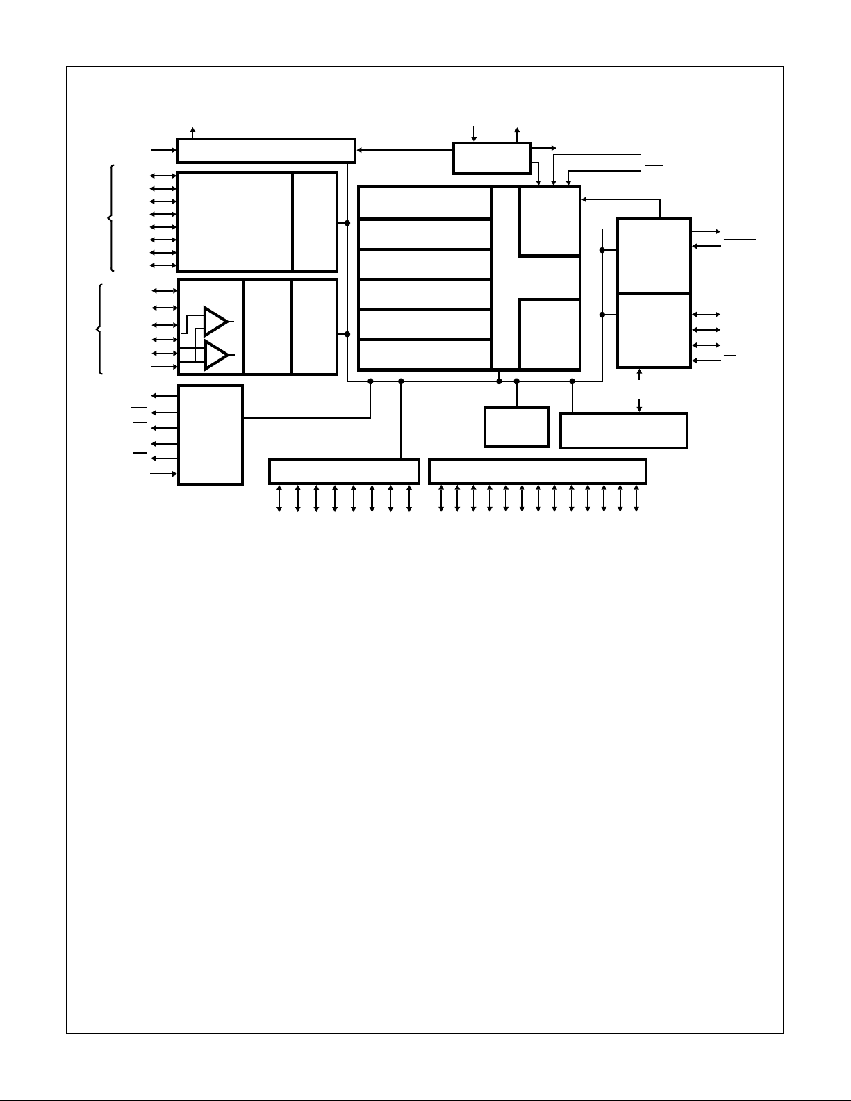
Block Diagram
HIP7030A0
34
TCAP
49
PA0
48
PA1
47
PA2
46
PA3
45
PA4
44
PA5
43
PA6
PORT A I/O LINES
PD2, V2
PD3, V3
PD4, VR
PORT D I/O LINES
PA7
PD0
PD1
TCAP
DS
WE
CE
FS
RD
ALC
42
19
18
17
16
15
13
12
14
TCMP OSCIN OSCOUT
35
TIMER SYSTEM
9
6
5
PORT D
REG
+
-
+
-
BUS
CONTROL
VSS22
VDD7
PORT
A
REG
PORT D
SFR
REG
DATA
DIR
REG
PORT D
DIR
REG
58575655545352
DB0
DB1
DB2
DB3
INTERNAL
PROCESSOR
CLOCK
ACCUMULATOR
8
INDEX
REGISTER
8
CONDITION CODE
5
REGISTER
STACK
6
POINTER
PROGRAM
COUNTER HIGH
5
PROGRAM
8
COUNTER LOW
51
DB4
DB5
DB6
OSCILLATOR
AND
A
X
CC
S
PCH
PCL
STATIC RAM
49484746454443
A0A1A2A3A4A5A6
DB7
÷ 2
ADDRESS DRIVEBUS DRIVE
176 x 8
2324
50
CPU
CONTROL
CPU
ALU
42
A7
OSCB
INTERNAL PROCESSOR CLOCK
WATCHDOG AND
SLOW CLOCK DETECT
4948474645
A8
38
39
SYMBOL INT
VPW SYMBOL
ENCODER /
DECODER
ARBITRATION
A9
A10
A11
RESET
IRQ
AND
SPI
SYSTEM
A12
37
36
32
26
25
33
VPWOUT
VPWIN
SCK
MOSI
MISO
SS
9-41
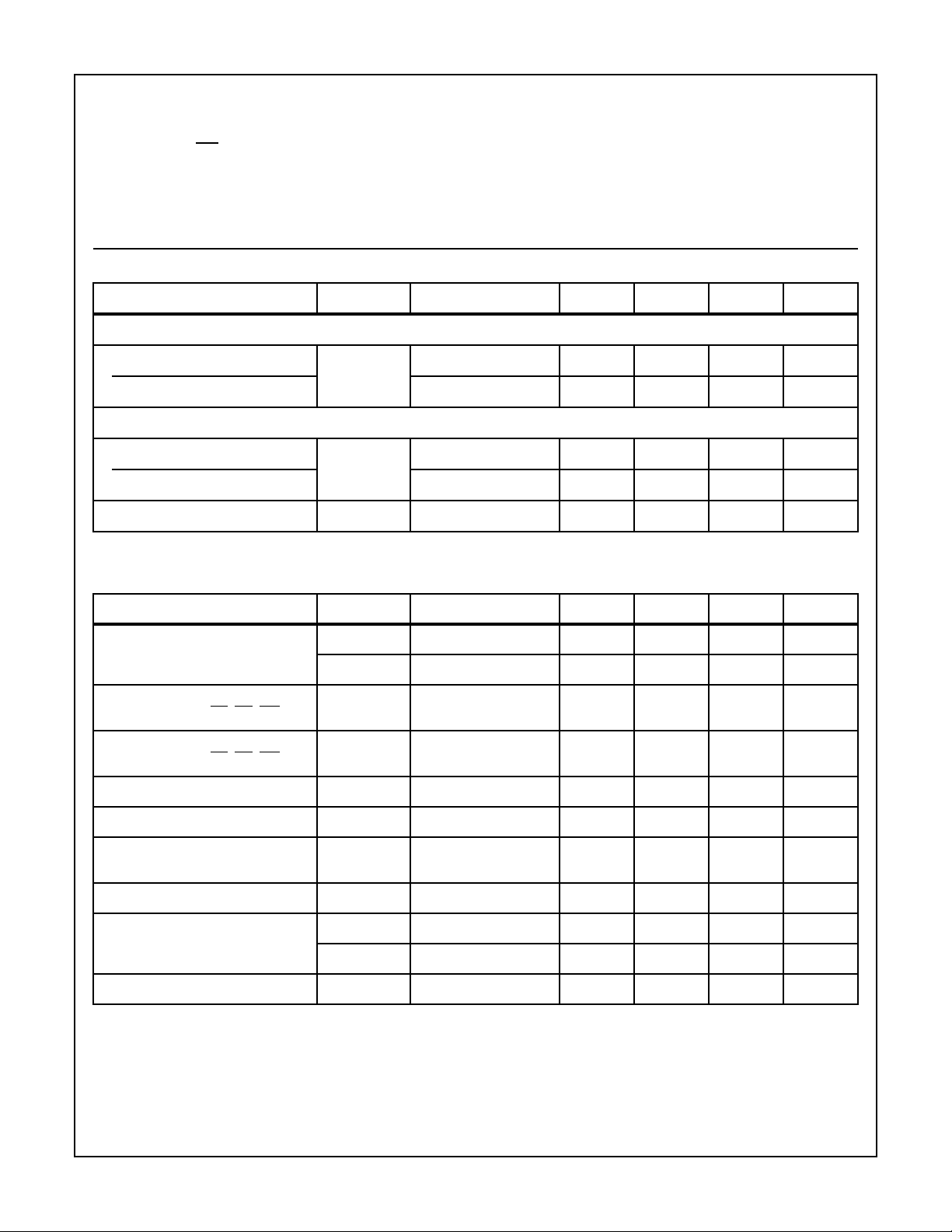
Specifications HIP7030A0
Absolute Maximum Ratings Thermal Information
DC Supply Voltage, VDD. . . . . . . . . . . . . . . . . . . . . . . . . .-0.5 to +7V
Input Voltage, VIN (Note 1). . . . . . . . . . . . . (VSS-0.3) to (VDD+0.3)V
Self-Check Mode (IRQ Pin Only), VIN . . (VSS-0.3) to 2•(VDD+0.3)V
Current Drain Per Pin (Excluding VDD and VSS) . . . . . . . . . . 25mA
CAUTION: Stresses above those listed in “Absolute Maximum Ratings” may cause permanent damage to the device. This is a stress only rating and operation
of the device at these or any other conditions above those indicated in the operational sections of this specification is not implied.
Thermal Resistance θ
JA
Plastic LCC Package. . . . . . . . . . . . . . . . . . . . . . . . . . . . .55oC/W
Maximum Package Power Dissipation, PDat 125oC . . . . . . 450mW
Operating Temperature Range . . . . . . . . . . . . . . . -40oC to +125oC
Storage Temperature Range, T
. . . . . . . . . . . -65oC to +150oC
STG
Lead Temperature (Soldering 10s) . . . . . . . . . . . . . . . . . . . . +265oC
Control Timing V
= 5VDC±10%, VSS = 0VDC, TA = -40oC to +125oC Unless Otherwise Specified.
DD
PARAMETER SYMBOL TEST CONDITION MIN TYP MAX UNITS
FREQUENCY OF OPERATION
Crystal Option f
OSC
1 - 10 MHz
External Clock Option 1 - 10 MHz
INTERNAL OPERATING FREQUENCY
Crystal (f
External Clock (f
Cycle Time t
DC Electrical Specifications V
+ 2) f
OSC
+ 2) 0.5 - 5 MHz
OSC
OP
CYC
= 5VDC±10%, VSS = 0VDC, TA = -40oC to +125oC Unless Otherwise Specified.
DD
0.5 - 5 MHz
200 - - ns
PARAMETER SYMBOL TEST CONDITION MIN TYP MAX UNITS
I
Output Voltage V
Output High Voltage:
OL
V
OH
V
OH
< 10mA - - 0.1 V
LOAD
I
> -10mA VDD -0.1 - - V
LOAD
I
= 0.8mA VDD -0.8 - - V
LOAD
A0-A12, DB0-DB7, CE, RD, WE, FS
Output Low Voltage:
A0-A12, DB0-DB7, CE, RD, WE, FS
Input High Voltage: DB0-DB7 V
Input Low Voltage: DB0-DB7 V
DB0-7 High Impedance Leakage
V
OH
IH
IL
I
IL
I
= 1.6mA - -
LOAD
- 0.5•V
0.3•V
-10 - +10 µA
DD
V
V
DD
0.4
0.7•V
DD
--V
Current:
Input Current I
Capacitance C
Supply Current: RUN I
IN
OUT
C
RUN
IN
-1 - +1 µA
- - 12 pF
--8pF
- 8 TBD mA
NOTES:
1. This device contains circuitry to protect the inputs against damage due to high static voltages of electric fields; however, i t is advised that
normal precautions be taken to avoid application of any voltage higher than maximum rated voltages to this high impedance circuit. For
proper operation it is recommended that VIN and V
be constrained to the range VSS ≤ (VIN or V
OUT
) ≤ VDD. Reliability of operation is
OUT
enhanced if unused inputs are connected to an appropriate logic voltage level (e.g., either VSS or VDD)
2. Characteristics are listed for the signals unique to the Emulator IC. For details on the other signal pins see the HIP7030A2 data sheet.
3. Minimum frequency applies when ALC is low.
9-42

Specifications HIP7030A0
Read Cycle Timing (ALC = 0) (See Figure 1) V
= 5VDC±10%, VSS = 0VDC, TA = -40oC to +125oC Unless Otherwise Specified.
DD
NUMBER SYMBOL PARAMETER MIN MAX UNITS
(1) t
(2) t
(3) t
(4) t
(5) t
(6) t
(7) t
(8) t
f
OSC
CYC
AVCEL
DVCEL
DVRDL
DVAV
CEHAX
CEHAX
RDLDX
OSCB Operating Frequency 1 10 MHz
Read Cycle Time 200 2000 ns
Address Setup Time Before CE -10 - ns
Access Time From CE - t
Access Time From RD - 0.75t
Access Time From Address Change - t
- 80 ns
CYC
- 80 ns
CYC
- 80 ns
CYC
Address Hold Time After CE 0 - ns
Data Hold Time After CE 0 - ns
Data Bus Driven From RD
0-ns
(Time to Data Active from High Impedance
State)
(9)
(10) t
t
RDHAX
OSCDS
Data Hold Time After RD
0-ns
(Hold Time to High Impedance State)
OSCB to DS Propagation Delay 5 25 ns
NOTE:
Minimum frequency applies when ALC is low.
Write Cycle Timing (ALC = 0) (See Figure 2) V
= 5VDC±10%, VSS = 0VDC, TA = -40oC to +125oC Unless Otherwise Specified.
DD
NUMBER SYMBOL PARAMETER MIN MAX UNITS
(1) t
(2) t
(3) t
(4) t
(5) t
(6) t
(7) t
(8) t
f
OSC
CYC
AVCEL
AVWEL
WEWE
DVWEH
WEHDX
WEHAX
OSCDS
OSCB Operating Frequency 1 10 MHz
Write Cycle Time 200 2000 ns
Address Setup Time Before CE -10 - ns
Address Setup Time Before WE 0.25t
WE Pulse Width 0.5t
Data Set-up Time to WE Trailing Edge 0.75t
Data Hold Time After WE Trailing Edge 0.25t
Address Hold Time After WE Trailing Edge 0.25t
- 25 - -
CYC
- 10 - ns
CYC
- 75 - ns
CYC
- 20 - ns
CYC
- 20 - ns
CYC
OSCB to DS Propagation Delay 5 25 ns
NOTE:
1. Minimum frequency applies when ALC is low.
Read Cycle Timing (ALC = 1) (See Figure 3) V
= 5VDC±10%, VSS = 0VDC, TA = -40oC to +125oC Unless Otherwise Specified.
DD
NUMBER SYMBOL PARAMETER MIN MAX UNITS
f
OSC
OSCB Operating Frequency 10 MHz
9-43

Specifications HIP7030A0
Read Cycle Timing (ALC = 1) (See Figure 3) V
= 5VDC±10%, VSS = 0VDC, TA = -40oC to +125oC Unless Otherwise Specified.
DD
NUMBER SYMBOL PARAMETER MIN MAX UNITS
(1) t
(2) t
(3) t
(4) t
(5) t
(6) t
(7) t
(8) t
CYC
RDOSC
DVCEL
DVOSC
OSCAV
OSCAX
OSCAX
RDLDX
Read Cycle Time 200 - ns
RD, FS Setup Time Before OSCB 0.5t
Access Time From CE - t
Access Time From OSCB - t
Address Setup Time Before OSCB 0.5t
Address Hold Time After OSCB 0.5t
-25 - ns
CYC
-80 ns
CYC
-70 ns
CYC
-25 - ns
CYC
CYC
-ns
Data Hold Time After OSCB 10 - ns
Data Bus Driven From CE
(Time to Data Active from High Impedance
0
-
State)
(9) t
(10) t
OSCRD
OSCDS
RD, FS Hold Time After OSCB 0.5t
CYC
-ns
OSCB to DS Propagation Delay 5 25 ns
NOTE:
1. Minimum frequency applies when ALC is high.
ns
Write Cycle Timing (ALC = 1) (See Figure 4) V
= 5VDC±10%, VSS = 0VDC, TA = -40oC to +125oC Unless Otherwise Specified.
DD
NUMBER SYMBOL PARAMETER MIN MAX UNITS
(1) t
(2) t
(3) t
(4) t
(5) t
(6) t
(7) t
f
OSC
CYC
RDOSC
DVOSC
OSCAV
OSCAX
OSCAX
OSCDX
OSCB Operating Frequency 10 MHz
Write Cycle Time 200 - ns
RD, FS Setup Time Before OSCB 0.5t
Data Setup Time Before OSCB 0.75t
Address Setup Time Before OSCB 0.5t
Address Hold Time After OSCB 0.5t
-25 - ns
CYC
-95 ns
CYC
-25 - ns
CYC
CYC
-ns
Data Hold Time After OSCB 10 - ns
Data Bus Driven From OSCB
.25t
CYC
-25 (Time to Data Active from High Impedance
State)
(8) t
(9) t
OSCRD
OSCDS
RD, FS Hold Time After OSCB 0.5t
CYC
-ns
OSCB to DS Propagation Delay 5 25 ns
NOTE:
1. Minimum frequency applies when ALC is high.
ns
9-44

OSCB
HIP7030A0
1
DS
A0-A12
CE
RD
DB
2 6
10
NOTE:
1. Measurement points are VOL, VOH, VIL and VIH.
FIGURE 1. READ CYCLE TIMING DIAGRAM (ALC = 0)
5
3
4
78
1
9
OSCB
DS
A0-A12
CE
WE
DB
2
8
3 4
NOTE:
1. Measurement points are VOL, VOH, VIL and VIH.
FIGURE 2. WRITE CYCLE TIMING DIAGRAM (ALC = 0)
7
6
5
9-45

HIP7030A0
OSCB
DS
A0-A12
CE
RD
DB
10
5
2
NOTES:
1. Measurement points are VOL, VOH, VIL and VIH.
2. Timing for FS is identical to RD timing.
FIGURE 3. READ CYCLE TIMING DIAGRAM (ALC = 1)
1
4
6
3
9
8
7
OSCB
DS
A0-A12
CE
RD
DB
9
NOTES:
1. Measurement points are V
, VOH, VIL and VIH.
OL
2. Timing for FS is identical to RD timing.
1
4
2
7
5
8
FIGURE 4. WRITE CYCLE TIMING DIAGRAM (ALC = 1)
6
3
9-46

OSCB
DS
A0-A12
CE
RD
WE
FS
DB
Functional Pin Description
HIP7030A0
FETCH READ (INTERNAL) WRITE
FIGURE 5. SIGNAL TIMING DIAGRAM (ALC = 1)
This section provides a brief description of each of the pins
of the HIP7030A0 microcontroller. A more detailed discussion is contained in the HIP7030A2 data sheet.
V
and VSS (Power)
DD
Power is supplied to the MCU using these two pins. V
connected to the positive supply and V
is connected to the
SS
DD
is
negative supply.
IRQ (Maskable Interrupt Request - Input)
IRQ pin is negative edge-sensitive triggering. A high to
The
low transition on the input to the
IRQ pin will produce an
interrupt.
In the event of an interrupt request, the MCU always com-
pletes the current instruction before it responds to the
request. An internal mask can be used to inhibit the MCU
from responding to
An edge-sensitive
pulled low for at least one t
going pulse is registered in a flip-flop and the
will be recognized even if the
IRQ interrupts.
IRQ interrupt is generated if the IRQ pin is
. The occurrence of the low
ILIH
IRQ interrupt
IRQ pin has returned to a high
state before the interrupt can be serviced.
Once the edge-sensitive flip-flop is cleared (it is automati-
cally cleared at the start of the interrupt service routine) the
interrupt request is removed until the
IRQ pin returns to a
high level and once again goes low.
RESET (Master Reset - Input)
The HIP7030A2 contains an integrated Power-On Reset (POR)
circuit and the
RESET input is therefore not required for startup. It can be used to reset the MCU internal state and provides for an orderly re-start of the software after initial powerup. A low level on the
RESET pin will reset the HIP7030A0.
TCAP (Timer Capture - Input)
The TCAP input controls the input capture feature for the onchip programmable timer system. The TCAP input is also
used as the strobe signal to the Port D strobed outputs.
TCMP (Timer Compare - Output)
The TCMP pin provides an output for the output compare
feature of the on-chip timer system.
OSCIN (Oscillator Input - Input),
OSCOUT (Oscillator Output - Output),
OSCB (Oscillator Buffered Output - Output)
OSCIN is the input and OSCOUT is the output of an inverter/
amplifier which can be used to build either a quartz crystal or
ceramic resonator based clock oscillator. Alternatively the
OSCIN input can be driven from any external clock source
which satisfies the CMOS schmitt trigger input level requirements of the OSCIN pin. OSCB is a squared, buffered version of the OSCIN signal, available for driving one external
CMOS load. See Electrical Specifications of the HIP7030A2
for output drive and input level specifications.
The fundamental internal clock is derived by a divide-by-two
of the external oscillator frequency (fOSC). All other internal
clocks are also derived from the external frequency. These
clocks include the input to the 16-bit Timer, the SPI Serial
Clock (SCK), and the VPW Symbol Encoder/Decoder (SENDEC).
PA0-PA7 (Port A - Input/Output)
These eight I/O lines comprise Port A. The mode (i.e. - input
or output) of each pin is software programmable. All Port A I/
O lines are configured as inputs during power-on or
RESET.
9-47

HIP7030A0
PD0-PD4 (Port D - Input/Output)
These five I/O lines comprise Port D. As with PA0-PA7, the
mode (i.e. - input or output) of each pin is software programmable. In addition a Special Function Register (SFRD)
allows configuring PD0 and PD1 as “strobed” outputs, and/or
PD2,PD3, and PD4 as inputs to an on-chip analog comparator.
All Port D I/O lines are configured as inputs during power-on
or
RESET.
VPWOUT (Variable Pulse Width Out - Output),
VPWIN (Variable Pulse Width In - Input)
These two lines are used to interface to the J1850 bus transceiver.
VPWOUT is the pulse width modulated output of the SENDEC encoder block.
VPWIN is the inverted input to the SENDEC decoder block.
MISO (Master-in/Slave-out - Input/Output),
MOSI (Master-out/Slave-in - Input/Output),
SCK (Serial Clock - Input/Output),
SS (Slave Select - Input)
These four lines constitute the Serial Peripheral Interface
(SPI) communications port. The MCU can be configured as
a SPI “master” or as a SPI “slave”. In master mode MOSI
and SCK function as outputs and MISO functions as an
input. In slave mode MOSI and SCK are inputs and MISO is
an output. SS is always an input.
Serial data words are transmitted and received over the
MISO/MOSI lines synchronously with the SCK clock stream.
The word size is fixed at 8 bits. Single buffering is used
which results in an inherent inter-byte delay. The master
device always provides the synchronizing clock.
A low on the
SS line causes the MCU to immediately
assume the role of slave, regardless of it’s current mode.
This allows multi-master systems to be constructed with
appropriate arbitration protocols.
ALC (Address Latch Control - Input)
The ALC input controls the timing and function of the
address and memory control lines (
CE, RD, WE, and FS).
For more information on each of these lines refer to the
appropriate section.
When ALC is low the address and control lines are produced
coincident with data bus transitions of the HIP7030A0’s
machine cycle. This mode allows direct interfacing to industry standard memory devices. Refer to the timing diagrams
in Electrical Specifications for more details.
Driving ALC high causes several changes in the behavior of
the address and control lines. These changes are intended
to facilitate design of development systems for the
HIP7030A2. When ALC is high the following occur:
• The Internal RAM is disabled and accesses to RAM space
are mapped off-chip.
• A0-A12, FS, and
RD are produced t
cycle (i.e. 100ns
CYC
with a 10MHz clock) ahead of data bus transitions of the
HIP7030A0’s machine cycle. The earlier availability of
these address and control lines facilitates implementation
of break detection and bus tracing logic. External latching
of the address and control signals is required for interfacing to the memory of the development tool. The timing of
CE and WE are not affected by ALC, and remain synchronized with data bus transfers.
RD signal is no longer gated with CE and is a full
• The
cycle wide, when ALC is high.
ensuing data bus cycle will be a
ory-I/O space. It can be viewed as a
vides
R/W information for all cycles, internal as well as
RD indicates whether the
read of
or
write to
mem-
R/W signal. RD pro-
external.
• Resetting the HIP7030A0 with ALC = 1 disables the Slow
Clock Detect circuits. The Watchdog can be disabled by
writing to the Watchdog Status Register (WSR - location
$1E), which has special features when ALC is high. The
Slow Clock circuit is permanently disabled when ALC = 1.
If the Slow Clock detect circuitry were allowed to run, stopping the CPU clock during breakpoint servicing would not
be possible. The watchdog should be reset by the tool
while interrogating the CPU.
The ALC input has an integrated pull-down device which
allows floating this pin when interfacing to industry standard
memory devices.
A0-A12
Address lines 0 through 12. When ALC = 0, A0-A12 are
coincident with data bus transfers. When ALC = 1, A0-A12
change t
ahead of the data bus transfers and must be
CYC
externally latched. See the timing diagrams in the Electrical
Specifications section for more details.
DB0-DB7
Bidirectional 8-bit non-multiplexed data bus lines. The data
bus is an input during all reads from external memory-I/O
space and during the first t
of every machine cycle. At all
CYC
other times it is an output. See the timing diagrams in the
Electrical Specifications section for more details.
CE (Chip Enable - Output)
Chip Enable is an output signal used for selecting external
memory or I/O. A low level indicates when external memory
or I/O is being accessed. Note that the
CE signal will not go
true when addressing the unused locations of Page 0 I/O
space even though the address lines will be valid.
RD (Read - Output)
RD is a status output signal which indicates direction of data
flow with respect to external or internal memory space (a low
level indicates a read from memory space). A read from
internal memory or I/O will place data on the external data
9-48

HIP7030A0
bus. When ALC = 0, RD is internally gated with CE, and generated in synchronization with data bus cycles. With ALC =
0, standard RAM, ROM, and EPROM devices can be directly
connected to the HIP7030A0 with no additional components.
When ALC = 1,
RD is not gated by CE and is produced t
CYC
cycle (i.e. 100ns with a 10MHz clock) ahead of data bus
transitions of the HIP7030A0’s machine cycle.
WE (Write Enable - Output)
Write Enable is an active low output pulse for use in writing
data to external RAM memory. A low level indicates valid
data on the data bus.
WE is internally gated with CE for writing to external memory. Since, in most systems, external
memory is substituting for mask programmed ROM,
WE is
frequently not used.
DS (Data Strobe - Output)
The Data Strobe output provides a pulse when address and
data are valid. DS can be used to transfer data to or from a
peripheral or memory and occurs every cycle and is also
used for synchronizing development tools to the oscillator
clock. DS is a continuous signal at f
÷ 2, except when the
OSC
Emulator is in the WAIT or STOP mode. See the timing diagrams in the Electrical Specifications section for more
details.
FS (Fetch Status - Output)
The FS output signal goes true to indicate an opcode fetch
cycle is in progress. When ALC = 0, FS will be coincident
with the data transfer of the fetch. When ALC = 1, FS is produced t
cycle (i.e. 100ns with a 10MHz clock) ahead of
CYC
data bus transitions of the HIP7030A0’s machine cycle. See
the timing diagrams in the Electrical Specifications section
for more details.
Watchdog Status Register
When ALC is high, the HIP7030A0’s Watchdog Status Register (WSR - location $1E) provides the ability to selectively
enable and disable the Watchdog Timer logic of the
HIP7030A0.
The user of a development tool should be cautioned against
accidently clearing the WDE bit of this register during final
code prove-out. During initial code development the user
may want to intentionally clear this bit to eliminate the need
to insert watchdog handling routines. The clearing of the bit
must be done following every reset.
Reset presets the WDE bit of the WSR to enable the Watchdog Timer.
76543210
- - - - - - WDE WDF
WATCHDOG STATUS REGISTER
Bit 7,6,5,4,3,2 - Unused
Bit 1 - WDE
When WDE (WatchDog Enable) is low , the W atchdog Timer is
disabled. When ALC is high, WDE is forced high by any reset.
The WDE bit should normally be cleared when servicing a
breakpoint (if OSCIN is being clocked), to avoid a Watchdog
Reset while interrogating the CPU.
The WDE bit controls the Watchdog Reset, but it doesn’t
inhibit the Watchdog Timer from advancing. Prior to reenabling the WDE bit, the Watchdog Timer should normally
be reset by writing $55, $AA to the Watchdog Reset Register
(WDRR, location $1D). This implies that each breakpoint
should generate a Watchdog Reset. To verify proper watchdog action the user should run final code with no breaks. In
some cases the number of CPU cycles utilized in the break
may be low enough to allow the watchdog to run without causing premature watchdog timeouts.
Bit 0 - WDF
The WatchDog flag (WDF), is set when a Watchdog timeout
causes a COP Reset. This flag is used to distinguish a Slow
Clock Detect from a Watchdog Timeout in the COP Reset service routine.
Writing a 0 to the Watchdog Reset Register (WDRR, location
$1D) clears the WDF flag. WDF is cleared by Power-on
Reset, but unaffected by all other types of resets. For this reason, WDF should normally be cleared (by writing a 0 to the
WDRR) following each read of the WSR.
All Intersil semiconductor products are manufactured, assembled and tested under ISO9000 quality systems certification.
Intersil products are sold by description only. Intersil Corporation reserves the right to make changes in circuit design and/or specifications at any time without
notice. Accordingly, the reader is cautioned to verify that data sheets are current before placing orders. Information furnished by Intersil is believed to be accurate
and reliable. However, no responsibility is assumed by Intersil or its subsidiaries for its use; nor for any infringements of patents or other rights of third parties which
may result from its use. No license is granted by implication or otherwise under any patent or patent rights of Intersil or its subsidiaries.
For information regarding Intersil Corporation and its products, see web site http://www.intersil.com
Sales Office Headquarters
NORTH AMERICA
Intersil Corporation
P. O. Box 883, Mail Stop 53-204
Melbourne, FL 32902
TEL: (407) 727-9207
FAX: (407) 724-7240
EUROPE
Intersil SA
Mercure Center
100, Rue de la Fusee
1130 Brussels, Belgium
TEL: (32) 2.724.2111
FAX: (32) 2.724.22.05
9-49
ASIA
Intersil (Taiwan) Ltd.
Taiwan Limited
7F-6, No. 101 Fu Hsing North Road
Taipei, Taiwan
Republic of China
TEL: (886) 2 2716 9310
FAX: (886) 2 2715 3029
 Loading...