

Intersil Corporation HIP7010 Datasheet
ADVANCE INFORMATION
August 1996
HIP7010
J1850 Byte Level Interface Circuit
Features
• Fully Supports VPW (Variable Pulse Width) Messa ging
Practices of SAE J1850 Standard for Class B Data
Communications Network Interface
- 3-Wire, High-Speed, Synchronous, Serial Interface
• Reduces Wiring Overhead
• Directly Interfaces with 68HC05 and 68HC11 Style SPI
Ports
• 1MHz, 8-Bit Transfers Between Host and HIP7010
Minimize Host Service Requirements
• Automatically Transmits Properly Framed Messages
• Prepends SOF to First Byte and Appends CRC to Last
Byte
• Fail-Safe Design Including, Slow Clock Detection
Circuitry, Prevents J1850 Bus Lockup Due to System
Errors or Loss of Input Clock
• Automatic Collision Detection
• End of Data (EOD), Break, Idle Bus, and Invalid Symbol
(Noise/Illegal Symbols) Detection
• Supports In-Frame Responses with Generation of
Normalization Bits (NB) for T ype 1, Type 2, and Type 3
Messages
• Wait-For-Idle Mode Reduces Host Overhead During
Non-Applicable Messages
• Status Register Flags Provide Information on Current
Status of J1850 Bus
• Serial I/O Pins are Active Only During Transfers - Bus
Available for Other Devices 95% of the Time
• TEST Pin Provides Built-in-Test Capabilities for
In-System Diagnostics and Factory Testing
• High Speed (4X) Receive Mode for Production and
Diagnostic Testing/Programming
• Operates with Wide Range of Input Clock Frequencies
• Power-Saving Power-Down Mode
• Full -40
• Single 3.0V to 6.0V Supply
o
C to +125oC Operating Range
Description
The Intersil HIP7010, J1850 Byte Level Interface Circuit, is a
member of the Intersil family of low-cost multiplexed wiring
ICs. The integrated functions of the HIP7010 provide the
system designer with components key to building a “Class B”
multiplexed communications network interface, which fully
conforms to the VPW Multiplexed Wiring protocol specified
in the SAE J1850 Standard. The HIP7010 is designed to
interface with a wide variety of Host microcontrollers via a
standard three wire, high-speed (1MHz), synchronous, serial
interface. The HIP7010 automatically produces properly
framed VPW messages, prepending the Start of Frame
(SOF) symbol and calculating and appending the CRC
check byte. All circuitry needed to decode incoming messages, to validate CRC bytes, and to detect Breaks, End of
Data (EOD), Idle bus, and illegal symbols is included. InFrame Responses (IFRs) are fully supported for Type 1,
Type 2, and Type 3 messages, with the appropriate Nor malization Bit automatically generated. The HCMOS design
allows proper opeSration at various input frequencies from
2MHz to 12MHz. Connection to the J1850 Bus is via a Intersil HIP7020.
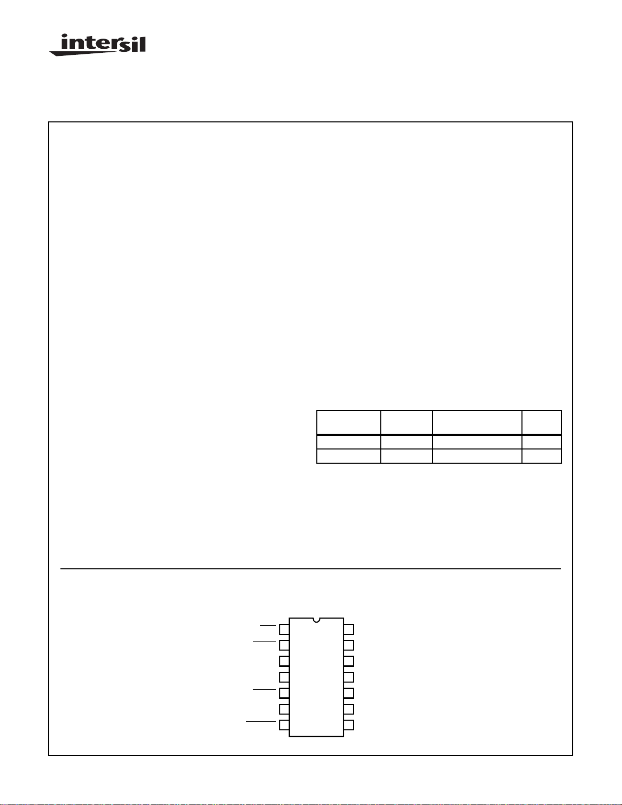
Ordering Information
TEMP.
P AR T NUMBER
HIP7010P -40 +125 14 Lead Plastic DIP E14.3
HIP7010B -40 +125 14 Lead Plastic SOIC (N) M14.15
RANGE (oC) P ACKAGE PKG. NO.
Pinout
HIP7010 (SOIC, PDIP)
TOP VIEW
IDLE
1
VPWIN
2
V
DD
RESET
TEST
3
4
5
6
7
1
VPWOUT
SACTIVE
CAUTION: These devices are sensitive to electrostatic discharge; follow proper IC Handling Procedures.
www.intersil.com or 407-727-9207
| Copyright © Intersil Corporation 1999
14
RDY
13
STAT
12
CLK
11
V
SS
SIN
10
SOUT
9
8
SCK
File Number 3644.2

Block Diagram
HIP7010
SIN
SOUT
10
9
SCK
IDLE
RDY
STAT
CLK
RESET
TEST
SACTIVE
MUX
A
B
MUX
C
A
B
8
1
14
13
12
5
6
7
LSB
DATA SHIFT REGISTER
DECODED VPW IN
STATUS/CONTROL BYTE
CRC GENERATOR/CHECKER
TIMING
GENERATOR
MSB
OUTPUT DATA
J1850 VPW SYMBOL
ENCODER/DECODER
STATE MACHINE
AND CONTROL LOGIC
3
VPWOUT
2
VPWIN
V
4
DD
11
V
SS
Pin Description
PIN NUMBER PIN NAME IN/OUT PIN DESCRIPTION
1 IDLE OUT CMOS Output
2 VPWIN IN CMOS Schmitt (No VDD Diode)
3 VPWOUT OUT CMOS Output
4VDD- Power Supply
5 RESET IN CMOS Schmitt (No VDD Diode)
6 TEST IN CMOS Input with Pull-Down
7 SACTIVE OUT CMOS Output
8 SCK OUT Three-State with Pull-Down
9 SOUT OUT Three-State with Pull-Down
10 SIN IN CMOS Input with Pull-Down
11 V
SS
12 CLK IN CMOS Schmitt (No VDD Diode)
- Ground
13 STAT IN CMOS Input with Pull-Down
14 RDY IN CMOS Input with Pull-Down
2

HIP7010
Absolute Maximum Ratings Thermal Information
Supply Voltage (VDD). . . . . . . . . . . . . . . . . . . . . . . . .-0.3V to +7.0V
Input or Output Voltage
Pins with VDD Diode. . . . . . . . . . . . . . . . . . . .-0.3V to VDD+0.3V
Pins without VDD Diode . . . . . . . . . . . . . . . . . . . .-0.3V to +10.0V
ESD Classification . . . . . . . . . . . . . . . . . . . . . . . . . . . . . . . . Class 2
Gate Count. . . . . . . . . . . . . . . . . . . . . . . . . . . . . . . . . . +2500 Gates
CAUTION: Stresses above those listed in “Absolute Maximum Ratings” may cause permanent damage to the device. This is a stress only rating and operation
of the device at these or any other conditions above those indicated in the operational sections of this specification is not implied.
Operating Conditions
Operating Voltage Range. . . . . . . . . . . . . . . . . . . . . +3.0V to +5.5V
Operating Temperature Range. . . . . . . . . . . . . . . .-40oC to +125oC
Input Low Voltage. . . . . . . . . . . . . . . . . . . . . . . . . . . . . . 0V to +0.8V
Thermal Resistance θ
JA
Plastic DIP Package . . . . . . . . . . . . . . . . . . . . . . . . . .+100oC/W
SOIC Package. . . . . . . . . . . . . . . . . . . . . . . . . . . . . . .+120oC/W
Maximum Package Power Dissipation at +125oC
DIP Package . . . . . . . . . . . . . . . . . . . . . . . . . . . . . . . . . . . 250mW
SOIC Package. . . . . . . . . . . . . . . . . . . . . . . . . . . . . . . . . .200mW
Operating Temperature Range (TA) . . . . . . . . . . . -40oC to +125oC
Storage Temperature Range (T
). . . . . . . . . . . -65oC to +150oC
STG
Junction Temperature . . . . . . . . . . . . . . . . . . . . . . . . . . . . . .+150oC
Lead Temperature (Soldering, 10s). . . . . . . . . . . . . . . . . . . .+265oC
Input High Voltage. . . . . . . . . . . . . . . . . . . . . . . . . .(0.8VDD) to V
DD
Input Rise and Fall Time
CMOS Inputs. . . . . . . . . . . . . . . . . . . . . . . . . . . . . . . . 100ns Max
CMOS Schmitt Inputs . . . . . . . . . . . . . . . . . . . . . . . . . . .Unlimited
Electrical Specifications T
= -40oC to +125oC, VDD = 5VDC±10%, Unless Otherwise Specified
A
PARAMETERS SYMBOL CONDITIONS MIN TYP MAX UNITS
Supply Current
Operating Current I
Power-Down Mode (Note 1) I
Clock Stopped (Note 2) I
OP
PD
STOP
CLK = 2.0 MHz - 1.0 5.0 mA
PD = 1 - 50 150 µA
CLK = VSS or V
DD
- 5.0 50 µA
Input High Voltage
CMOS Level (SIN, STAT, RDY, TEST) V
IH
Schmitt Trigger (RESET, CLK, VPWIN) 0.8V
0.7V
DD
DD
-VDDV
-VDDV
Input Low Voltage
CMOS Level (SIN, STAT, RDY, TEST) V
IL
Schmitt Trigger (RESET, CLK, VPWIN) V
V
SS
SS
- 0.3V
- 0.2V
High Level Input Current
(CLK, VPWIN, RESET) I
IH
VIN = V
DD
-1 0.001 1 µA
Input Buffer with Pull-Down (SIN, TEST, STAT, RDY) 100 200 500 µA
Low Level Input Current
(CLK, VPWIN, RESET) I
VIN = V
IL
SS
-1 -0.001 1 µA
Input Buffer with Pull-Down (SIN, TEST, STAT, RDY) -10 -0.01 10 µA
Output High Voltage
(SCK, SOUT, VPWOUT, IDLE, SACTIVE) V
OH
I
= 0.8 mA VDD-0.8 - - V
LOAD
Output Low Voltage
(SCK, SOUT, VPWOUT, IDLE, SACTIVE) V
OL
I
= -1.6 mA - - 0.4 V
LOAD
High Impedance Leakage Current
Three-State with Pull-Down (SCK, SOUT) I
Schmitt Trigger Hysteresis Voltage
V
OZ
HYS
V
V
OUT
OUT
= V
= V
DD
SS
100 200 500 µA
-10 10 µA
0.2 0.5 2.0 V
(RESET, CLK, VPWIN)
NOTES:
1. SIN, STAT, RDY, and TEST = VSS; SACTIVE, SCK, and SOUT unconnected; VPWIN = VDD; CLK = 10MHz.
2. SIN, STAT, RDY, and TEST = VSS; SACTIVE, SCK, and SOUT unconnected; VPWIN = VDD; PD = 1.
DD
DD
V
V
3

HIP7010
Serial Interface Timing (See Figure 1- Figure 7) T
= -40oC to +125oC, VDD = 5VDC±10%, Unless Otherwise Specified
A
NUMBER SYMBOL PARAMETERS MIN TYP MAX UNITS
- - Operating Frequency 2 8 12 MHz
- - Input CLK Duty Cycle 40 50 60 %
(1) t
(2) t
CYC
LEAD
SCK Cycle Time - 1.0 - MHz
SACTIVE Lead Time
Before Status/Control Transfer 450 750 850 ns
Before Data Transfer 1150 1225 1300 ns
(3) t
LAG
SACTIVE Lag Time
After Status/Control Transfer 650 750 850 ns
After Data Transfer 1250 1300 1400 ns
(4) t
(5) t
(6) t
(7) t
(8) t
(9) t
SCKH
SCKL
DVSCK
SCKDX
DZDA
DADZ
Clock (SCK) HIGH Time 450 500 550 ns
Clock (SCK) LOW Time 450 500 550 ns
Required Data In Setup Time (SIN to SCK) - 10 50 ns
Required Data In Hold Time (SIN after SCK) - -10 40 ns
Data Active from High Impedance Delay (SACTIVE to SOUT Active) -10 10 - ns
Data Active to High Impedance Delay (SACTIVE to SOUT High
-1040ns
Impedance)
(10) t
(11) t
(12) t
(13) t
(14) t
(15) t
(16) t
DVSCK
DXSCK
RISE
FALL
STATH
RDYH
t
RESETL
SACTIVE
Data Out Setup Time (SOUT to SCK) 375 475 - ns
Data Out Hold Time (SOUT after SCK) 375 475 - ns
Output Rise Time (0.3VDD to 0.7VDD, CL = 100pF) 15 75 150 ns
Output Fall Time (0.7VDD to 0.3VDD, CL = 100pF) 72575 ns
Required STAT Pulse Width - 20 75 ns
Required RDY Pulse Width - 20 75 ns
Required RESET Pulse Width - 20 75 ns
SACTIVE Delay from RDY (IDLE = VSS) 1150 1750 2450 ns
SACTIVE Delay from STAT (FTU = 0) 5 285 900 ns
(17) t
(18) t
(19) t
RDYSCK
SCKRDY
REC
Required RDY Removal Time Prior to Last SCK for Short RDY - 25 100 ns
Required RDY Hold Time after Last SCK for Long RDY - 0 100 ns
Required SERIAL Recovery Time (Minimum Time after SACTIVE
- 675 750 ns
Until Next RDY/STAT)
f
SLOW
Slow clock detect frequency limit 20 80 200 KHz
NOTE:
1. All parameters are specifications of the HIP7010 component not of a system. Parameters specified as “Required” (i.e ., t
STATH
the requirements of the HIP7010. If a “Required” pulse width is specified as 75ns maximum, that implies that 75ns is the maximum width
that any HIP7010 device will require. Therefore, a system that provides a minimum pulse width of 75ns will satisfy this maximum
requirement.
) refer to
4

STAT
(INPUT)
RDY (SHORT)
(INPUT)
RDY (LONG)
(INPUT)
SACTIVE
(OUTPUT)
HIP7010
(14)
(15)
(16) (17) (18)
(19)
(2)
SCK
(OUTPUT)
(4)
SOUT
(OUTPUT)
(10)
SIN
(INPUT)
(6)
(5)
D7O
(11)(8)
D7I D6I D0I
(7)
D6O D0O
FIGURE 1. SERIAL INTERFACE TIMING DIAGRAM
NOTES:
1. Measurement points are from VDD/2, except 12 and 13 which are measured between VIL and V
2. All timings assume proper CLK frequency and Divide Select values to generate 1MHz SCK.
Functional Pin Description
This section provides a description of each of the 14 pins of
the HIP7010 as shown in Figure 2.
IDLE
VPWIN
VPWOUT
V
DD
RESET
TEST
SACTIVE
1
2
3
4
5
6
7
14
RDY
13
STAT
12
CLK
11
V
SS
SIN
10
SOUT
9
8
SCK
FIGURE 2. 14 PIN DIP AND SO TERMINAL ASSIGNMENTS
V
and VSS (Power)
DD
Power is supplied to the HIP7010 using these two pins. V
is connected to the positive supply and VSS is connected to
the negative supply.
CLK (Clock - Input)
The Clock input (CLK) provides the basic time base reference for all J1850 symbol detection and generation. Serial
Bus transfers between the HIP7010 and the Host microcontroller are also timed based on the Clock input. Proper VPW
symbol detection and generation requires a 2MHz clock
which is internally derived from the CLK input. Various CLK
input frequencies can be accommodated via the Divide
Select bits in the Status/Control Register (see Status/Con-
trol Register for details).
An internal Slow Clock Detect circuit monitors the CLK input
signal and generates a HIP7010 reset if the clock is inactive
for more than 1/f
SLOW
blocking the J1850 and Serial busses in the event of a clock
failure. The Slow Clock Detect reset can also be intentionally
invoked by externally inhibiting CLK input transitions.
Pow er can be reduced under Host control via the PowerDown
bit in the Status/Control Register (see Status/Control Regis-
DD
ter for details). Setting the Power-Down bit effectively stops
internal clocking of the HIP7010.
(12)(13)(1)
IH.
(3)
(9)
. This is a safety mechanism to prevent
5

HIP7010
For enhanced noise immunity, the CLK input is a CMOS Schmitt
trigger input. See Electrical Specifications for input lev els .
VPWOUT (Variable Pulse Width Out - Output),
VPWIN (Variable Pulse Width In - Input)
These two lines are used to interface to a J1850 bus transceiver, such as the Intersil HIP7020. VPWOUT is the variable pulse width modulated output of the HIP7010’s symbol
encoder circuit.
decoder of the HIP7010.
SIN (Serial In - Input),
SOUT (Serial Out - Output),
SCK (Serial Clock - Output),
SACTIVE (Serial Bus Active - Output)
These four lines constitute the synchronous Serial Interface
(SERIAL) interface of the HIP7010. See the Serial Interface
(SERIAL) System for details. SIN, SOUT, and SCK provide
the three principal connections to the Host controller. SIN is a
CMOS input. SOUT and SCK are three-state outputs which
are only activated during serial transfers. The SIN, SOUT, and
SCK pins contain integrated pull-down load devices which
provide termination on the bus whenever it is in a high impedance state. The SACTIVE pin is a CMOS output, which pulls
low when the HIP7010 is communicating on the serial bus.
See Serial Interface (SERIAL) System and Applications
Information for more details.
RDY (Byte Ready - Input)
The Byte Ready (RDY) line is a “handshaking” input from the
Host. Each rising edge on the RDY pin signifies that the Host
has loaded a byte into its SERIAL transmit register and the
HIP7010 can retrieve it (by generating clocks on SCK) when
the HIP7010 is ready for the data. See Serial Interface
(SERIAL) System and Applications Information for more
details.
The RDY pin contains an integrated pull-down load device
which will hold the pin low if it is left unconnected.
IDLE (Idle/Service Request - Output)
IDLE output pin indicates that the J1850 Bus has been
The
in a passive state for at least 275µs and is now idle. If the
bus has been passive for a minimum of 239µs and another
node initiates a new message,
In its role as a Service Request pin, a reset forces
high. Following the reset,
cycles and is then driven low.
CLK cycles +1.5µs after completion of the first Status/Control byte transfer. The
role, remaining high until a 275µs lull (or 239µs plus a passive to active transition) has been detected on the J1850
bus. This provides a handshake mechanism to ensure the
Host will reinitialize the HIP7010 each time the HIP7010 is
reset via POR,
IDLE is low when an echo failure causes the ERR bit to be
If
set in the Status byte, the
and then return low (see Status/Control Register).
VPWIN is the inverted input to the symbol
VPWIN is a Schmitt input.
IDLE will pulse low for 1µs.
IDLE
IDLE remains high for 17 CLK
IDLE will remain low until 40
IDLE pin will then resume its normal
RESET, or Slow Clock Detect.
IDLE pin will pulse high for 2µs
If
IDLE is low when the host sets the NXT bit in the control
byte, the
(see Status/Control Register).
In general a Status/Control byte transfer should be performed
each time IDLE goes low . SeeEffects of Resets and Power-
Down and Applications Information for more details.
The
of the HIP7010 for more details.
STAT (Request Status/Control - Input)
The Request Status/Control (STAT) input pin is used by the
Host microcontroller to initiate an exchange of the Host’s control byte and the HIP7010’s status byte. A low to high transition on the STAT input signals the HIP7010 that the Host has
placed a control word in it’s SERIAL output register and is
ready to exchange it with the HIP7010’s status word. The
HIP7010 controls the exchange by generating the 8 SCKs
required. See Serial Interface (SERIAL) System and Appli-
cations Information for more details.
The STAT pin contains an integrated pull-down load device
which will hold the pin low if it is left unconnected.
RESET (Reset - Input)
The
HIP7010. Resetting the HIP7010 forces
ables the SOUT and SCK pins, forces the VPWOUT output
low , drives
to its initial state. Following reset, the HIP7010 is inhibited
from transmitting or receiving J1850 messages until a Status/Control Register transfer has been completed (see
Effects Of Resets And Power-Down for more details).
The HIP7010 is also reset during initial power-on, by an
internal power-on-reset (POR) circuit.
Loss of a clock on the CLK input will cause a reset as
described previously under CLK.
If not used, the
For enhanced noise immunity, the
Schmitt trigger input. See Electrical Specifications for
input levels.
TEST (Test Mode - Input)
The TEST input provides a convenient method to test the
HIP7010 at the component level. Raising the TEST pin to a
high level causes the HIP7010 to enter a special TEST mode.
In the TEST mode, a special portion of the state machine is
activated which provides access to the Built-in-Test and diagnostic capabilities of the HIP7010 (see Test Mode for more
details).
The TEST pin contains an integrated pull-down load device
which will hold the pin low if it is left unconnected. In many
applications the TEST pin will be left unconnected, to allow
access via a board level ATE tester.
IDLE pin will pulse high for 2µs and then return low
IDLE pin is an active low CMOS output. See Operation
RESET input is a low level active input, which resets the
SACTIVE high, dis-
IDLE high, and returns the internal state machine
RESET pin should be tied to VDD.
RESET input is a CMOS
6
 Loading...