intersil HIP6601B, HIP6603B, HIP6604B DATA SHEET

HIP6601B, HIP6603B, HIP6604B
S
®
D
N
E
M
M
O
C
E
R
T
O
N
L
S
I
E
T
N
I
S
I
,
2
1
6
6
R
L
I
S
R
2
1
6
6
L
1
6
6
L
S
I
R
O
F
D
E
Data Sheet July 20, 2005
A
4
M
M
O
C
E
6
L
S
I
,
6
L
S
I
,
D
W
E
N
S
D
N
E
S
I
,
3
1
6
A
4
1
6
N
G
I
S
E
:
L
,
A
3
1
6
6
FN9072.7
Synchronous Rectified Buck
MOSFET Drivers
The HIP6601B, HIP6603B and HIP6604B are highfrequency, dual MOSFET drivers specifically designed to
drive two power N-Channel MOSFETs in a synchronous
rectified buck converter topology. These drivers combined
with a HIP63xx or the ISL65xx series of Multi-Phase Buck
PWM controllers and MOSFETs form a complete corevoltage regulator solution for advanced microprocessors.
The HIP6601B drives the lower gate in a synchronous
rectifier to 12V, while the upper gate can be independently
driven over a range from 5V to 12V. The HIP6603B drives
both upper and lower gates over a range of 5V to 12V. This
drive-voltage flexibility provides the advantage of optimizing
applications involving trade-offs between switching losses
and conduction losses. The HIP6604B can be configured as
either a HIP6601B or a HIP6603B.
The output drivers in the HIP6601B, HIP6603B and
HIP6604B have the capacity to efficiently switch power
MOSFETs at frequencies up to 2MHz. Each driver is
capable of driving a 3000pF load with a 30ns propagation
delay and 50ns transition time. These products implement
bootstrapping on the upper gate with only an external
capacitor required. This reduces implementation complexity
and allows the use of higher performance, cost effective,
N-Channel MOSFETs. Adaptive shoot-through protection is
integrated to prevent both MOSF ETs fro m conducting
simultaneously.
Features
• Drives Two N-Channel MOSFETs
• Adaptive Shoot-Through Protection
• Internal Bootstrap Device
• Supports High Switching Frequency
- Fast Output Rise Time
- Propagation Delay 30ns
• Small 8 LD SOIC and EPSOIC and 16 LD QFN Packages
• Dual Gate-Drive Voltages for Optimal Efficiency
• Three-State Input for Output Stage Shutdown
• Supply Undervoltage Protection
• QFN Package
- Compliant to JEDEC PUB95 MO-220 QFN—Quad Flat
No Leads—Product Outline.
- Near Chip-Scale Package Footprint; Improves PCB
Efficiency and Thinner in Profile.
Applications
• Core Voltage Supplies for Intel Pentium® III, AMD®
Athlon™ Microprocessors
• High Frequency Low Profile DC-DC Converters
• High Current Low Voltage DC-DC Converters
Related Literature
• Technical Brief TB363, Guidelines for Handling and
Processing Moisture Sensitive Surface Mount Devices
(SMDs)
1
CAUTION: These devices are sensitive to electrostatic discharge; follow proper IC Handling Procedures.
1-888-INTERSIL or 1-888-468-3774
| Intersil (and design) is a registered trademark of Intersil Americas Inc.
Copyright © Intersil Americas Inc. 2002-2005. All Rights Reserved.
All other trademarks mentioned are the property of their respective owners.

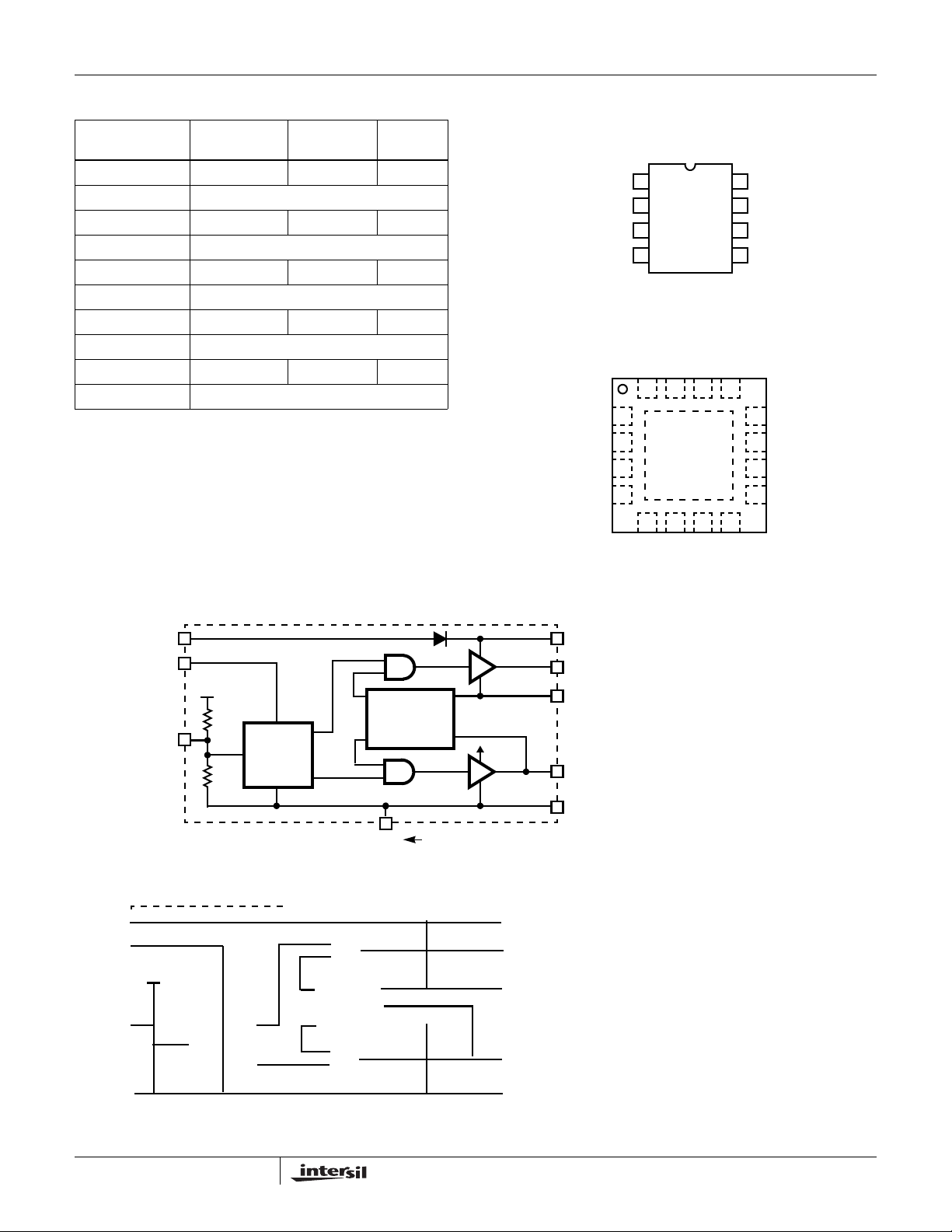
Ordering Information
TEMP. RANGE
PART NUMBER
(°C) PACKAGE
HIP6601BCB 0 to 85 8 Ld SOIC M8.15
HIP6601BCB-T 8 Ld SOIC Tape and Reel
HIP6601BECB 0 to 85 8 Ld EPSOIC M8.15B
HIP6601BECB-T 8 Ld EPSOIC Tape and Reel
HIP6603BCB 0 to 85 8 Ld SOIC M8.15
HIP6603BCB-T 8 Ld SOIC Tape and Reel
HIP6603BECB 0 to 85 8 Ld EPSOIC M8.15B
HIP6603BECB-T 8 Ld EPSOIC Tape and Reel
HIP6604BCR 0 to 85
16 Ld 4x4 QFN
HIP6604BCR-T 16 Ld 4x4 QFN Tape and Reel
PKG.
DWG. #
L16.4x4
Block Diagrams
HIP6601B AND HIP6603B
PVCC
VCC
+5V
SHOOT-
THROUGH
PROTECTION
PWM
10K
CONTROL
LOGIC
10K
Pinouts
†
HIP6601BCB, HIP6603BCB (SOIC)
HIP6601ECB, HIP6603ECB (EPSOIC)
TOP VIEW
UGATE
BOOT
PWM
GND
1
2
3
4
8
7
6
5
PHASE
PVCC
VCC
LGATE
HIP6604B (QFN)
TOP VIEW
NC
BOOT
PWM
GND
BOOT
UGATE
PHASE
LGATE
UGATENCPHASE
15
16 14 13
1
2
3
4
6578
NC
PGND
† VCC FOR HIP6601B
PVCC FOR HIP6603B
NC
12
11
10
9
NC
LGATE
NC
PVCC
LVCC
VCC
GND
PAD
FOR HIP6601ECB AND HIP6603ECB DEVICES, THE PAD ON THE BOTTOM
SIDE OF THE PACKAGE MUST BE SOLDERED TO THE PC BOARD.
HIP6604B QFN PACKAGE
2
FN9072.7
July 20, 2005

HIP6601B, HIP6603B, HIP6604B
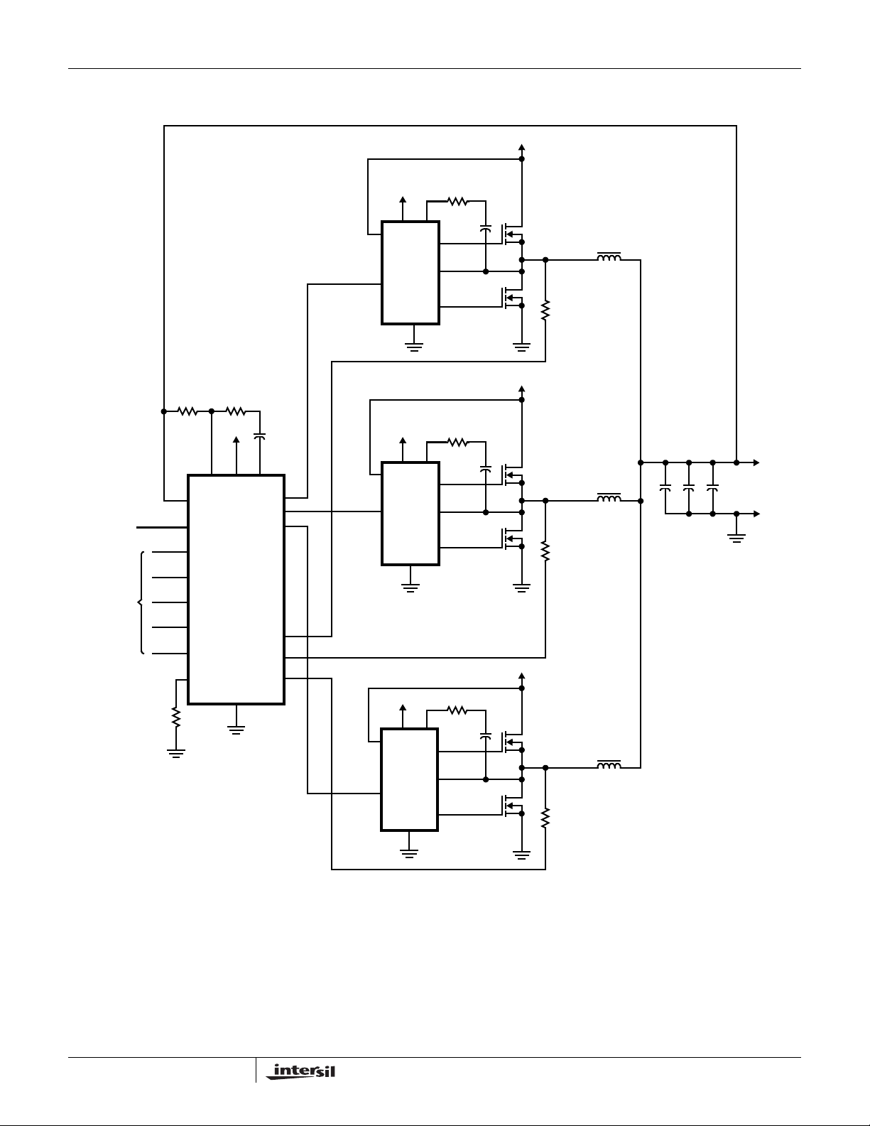
Typical Application: 3-Channel Converter Using HIP6301 and HIP6601B Gate Drivers
+12V
+5V
BOOT
VCC
PWM
PVCC
DRIVE
HIP6601B
UGATE
PHASE
LGATE
+12V
PGOOD
VID
VFB
VSEN
FS
+5V
VCC
MAIN
CONTROL
HIP6301
GND
COMP
PWM1
PWM2
PWM3
ISEN1
ISEN2
ISEN3
VCC
PWM
VCC
PWM
+5V
PVCC
DRIVE
HIP6601B
+5V
PVCC
DRIVE
HIP6601B
BOOT
UGATE
PHASE
LGATE
BOOT
UGATE
PHASE
LGATE
+12V
+V
CORE
3
FN9072.7
July 20, 2005

HIP6601B, HIP6603B, HIP6604B
Absolute Maximum Ratings
Supply Voltage (VCC) . . . . . . . . . . . . . . . . . . . . . . . . . . . . . . . . .15V
Supply Voltage (PVCC) . . . . . . . . . . . . . . . . . . . . . . . . . VCC + 0.3V
BOOT Voltage (V
Input Voltage (V
UGATE. . . . . . .V
. . . . . . . . . . . .V
LGATE. . . . . . . . . GND - 5V(<400ns pulse width) to V
. . . . . . . . . . . . . . GND -0.3V(>400ns pulse width) to V
PHASE. . . . . . . . . . . . . . . . . . GND -5V(<400ns pulse width) to 15V
. . . . . . . . . . . . . . . . . . . . . . .GND -0.3V(>400ns pulse width) to 15V
ESD Rating
Human Body Model (Per MIL-STD-883 Method 3015.7) . . . . .3kV
Machine Model (Per EIAJ ED-4701 Method C-111) . . . . . . .200V
- V
BOOT
) . . . . . . . . . . . . . . . . . . . . . . GND - 0.3V to 7V
PWM
- 5V(<400ns pulse width) to V
PHASE
-0.3V(>400ns pulse width) to V
PHASE
) . . . . . . . . . . . . . . . . . . . . . . .15V
PHASE
BOOT
BOOT
PVCC
PVCC
+ 0.3V
+ 0.3V
+ 0.3V
+ 0.3V
Thermal Information
Thermal Resistance θJA (°C/W) θJC (°C/W)
SOIC Package (Note 1) . . . . . . . . . . . . 97 N/A
EPSOIC Package (Note 2). . . . . . . . . . 38 N/A
QFN Package (Note 2). . . . . . . . . . . . . 48 10
Maximum Junction Temperature (Plastic Package) . . . . . . . .150°C
Maximum Storage Temperature Range . . . . . . . . . .-65°C to 150°C
Maximum Lead Temperature (Soldering 10s). . . . . . . . . . . . .300°C
(SOIC - Lead Tips Only)
For Recommended soldering conditions see Tech Brief TB389.
Operating Conditions
Ambient Temperature Range . . . . . . . . . . . . . . . . . . . . 0°C to 85°C
Maximum Operating Junction Temperature . . . . . . . . . . . . . 125°C
Supply Voltage, VCC. . . . . . . . . . . . . . . . . . . . . . . . . . . . 12V ±10%
Supply Voltage Range, PVCC . . . . . . . . . . . . . . . . . . . . . 5V to 12V
CAUTION: Stresses above those listed in “Absolute Maximum Ratings” may cause permanent damage to the device. This is a stress only rating and operation of the
device at these or any other conditions above those indicated in the operational sections of this specification is not implied .
NOTES:
is measured with the component mounted on a high effective thermal conductivity test board in free air. See Tech Brief TB379 for details.
1. θ
JA
2. θ
is measured in free air with the component mounted on a high effective thermal conductivity test board with “direct attach” features. θ
JA
“case temp” is measured at the center of the exposed metal pad on the package underside. See Tech Brief TB379.
JC,
the
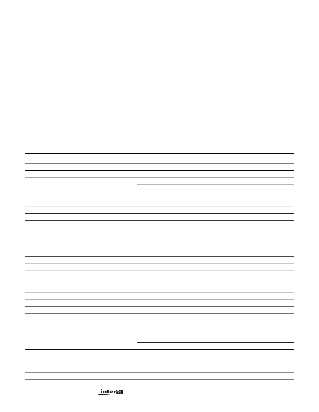
Electrical Specifications Recommended Operating Conditions, Unless Otherwise Noted
PARAMETER SYMBOL TEST CONDITIONS MIN TYP MAX UNITS
VCC SUPPLY CURRENT
Bias Supply Current I
Upper Gate Bias Current I
VCC
PVCC
POWER-ON RESET
VCC Rising Threshold 9.7 9.95 10.4 V
VCC Falling Threshold 7.3 7.6 8.0 V
PWM INPUT
Input Current I
PWM
PWM Rising Threshold -3.6- V
PWM Falling Threshold -1.45- V
UGATE Rise Time t
LGATE Rise Time t
UGATE Fall Time t
LGATE Fall Time t
UGATE Turn-Off Propagation Delay t
LGATE Turn-Off Propagation Delay t
RUGATEVPVCC
RLGATEVPVCC
FUGATEVPVCC
FLGATEVPVCC
PDLUGATEVPVCC
PDLLGATEVPVCC
Shutdown Window 1.4 - 3.6 V
Shutdown Holdoff Time - 230 - ns
OUTPUT
Upper Drive Source Impedance R
Upper Drive Sink Impedance R
Lower Drive Source Current
Equivalent Drive Source Impedance
Lower Drive Sink Impedance R
UGATEVPVCC
UGATEVPVCC
I
LGATE
R
LGATE
LGATEVPVCC
HIP6601B, f
HIP6603B, f
HIP6601B, f
HIP6603B, f
V
= 0V or 5V (See Block Diagram) - 500 - µA
PWM
PWM
PWM
PWM
PWM
= 1MHz, V
= 1MHz, V
= 1MHz, V
= 1MHz, V
= 12V - 4.4 6.2 mA
PVCC
= 12V - 2.5 3.6 mA
PVCC
= 12V - 200 430 µA
PVCC
= 12V - 1.8 3.3 mA
PVCC
= 12V, 3nF Load - 20 - ns
= 12V, 3nF Load - 50 - ns
= 12V, 3nF Load - 20 - ns
= 12V, 3nF Load - 20 - ns
= 12V, 3nF Load - 30 - ns
= 12V, 3nF Load - 20 - ns
= 5V - 1.7 3.0 Ω
V
= 12V - 3.0 5.0 Ω
PVCC
= 5V - 2.3 4.0 Ω
V
= 12V - 1.1 2.0 Ω
PVCC
V
= 5V 400 580 - mA
PVCC
= 12V 500 730 - mA
V
PVCC
V
= 5V - 9 - Ω
PVCC
= 5V or 12V - 1.6 4.0 Ω
4
FN9072.7
July 20, 2005
 Loading...