

Page 1
HIP6502
Data Sheet December 1999 File Number 4775.1
Multiple Linear Power Controller with
ACPI Control Interface
The HIP6502 complements either an HIP6020 or an
HIP6021 in ACPI-compliant designs for microprocessor and
computer applications. The IC integrates four linear
controllers/regulators, switching, monitoring and control
functions into a 20-pin SOIC package. One linear controller
generates the 3.3V
/3.3VSBvoltage plane from the ATX
DUAL
supply’s 5VSB output, powering the south bridge and the
PCI slots through an external pass transistor during sleep
states (S3, S4/S5). A second transistor is used to switch in
the ATX 3.3V output for operation during S0 and S1/S2
(active) operating states. Two linear controllers/regulators
supply a choice of either or both of the computer system’s
2.5V or 3.3V memory power through external pass
transistors in active states. During sleep states, integrated
pass transistors supply the sleep power. Another controller
powers up the 5V
plane by switching in the ATX 5V
DUAL
output in active states, and the ATX 5VSB in sleep states.
One internal regulator outputs a dedicated, noise-free 2.5V
clock chip supply. The HIP6502’s operating mode (active
outputs or sleep outputs) is selectable through two digital
control pins,
5V
DUAL
state, the 3.3V
S3 and S5. Enabling sleep state support on the
output is offered through the EN5VDL pin. In active
DUAL
and 3.3V
linear regulators use
MEM
external N-channel pass MOSFETs to connect the outputs
directly to the 3.3V input supplied by an ATX (or equivalent)
power supply, for minimal losses. In sleep state, power
delivery on both outputs is transferred to NPN transistors external to the controller on the 3.3V
3.3V
. Active state regulation on the 2.5V
MEM
, internal on the
DUAL
MEM
output is
performed through an external NPN transistor. In sleep
state, conduction on this output is transferred to an internal
pass transistor. The 5V
output is powered through two
DUAL
external MOS transistors. In sleep states, a PMOS (or PNP)
transistor conducts the current from the ATX 5VSB output;
while in active state, current flow is transferred to an NMOS
transistor connected to the ATX 5V output. The operation of
the 5V
output is dictated not only by the status of the
DUAL
S3 and S5 pins, but that of the EN5VDL pin as well. The
3.3V
5VSB voltage is applied to the chip. The 2.5V
/3.3VSB output is active for as long as the ATX
DUAL
CLK
output is
only active during S0 and S1/S2, and uses the 3V3 pin as
input source for its internal pass element.
Ordering Information
Features
• Provides 5 ACPI-Controlled Voltages
-5V
- 3.3V
- 2.5V
- 3.3V
- 2.5V
USB/Keyboard/Mouse (Active/Sleep)
DUAL
/3.3VSB PCI/Auxiliary/LAN (Active/Sleep)
DUAL
RDRAM (Active/Sleep)
MEM
SDRAM (Active/Sleep)
MEM
Clock/Processor Terminations (Active Only)
CLK
• Excellent Output Voltage Regulation
- 3.3V
/3.3VSB Output: ±2.0% Over Temperature;
DUAL
Sleep State Only
- 2.5V
Temperature; Both Operational States (3.3V
MEM
and 3.3V
Output: ±2.0% Over
MEM
MEM
in
sleep only)
- 2.5V
Output: ±2.0% Over Temperature
CLK
• Small Size
- Very Low External Component Count
• Dual Memory Voltage Support Via MSEL Pin
- 2.5V for RDRAM Memory
- 3.3V for SDRAM Memory
- Both 2.5V and 3.3V for Flexible Systems
• Under-Voltage Monitoring of All Outputs with Centralized
FAULT Reporting and Temperature Shutdown
Applications
•
Motherboard Power Regulation for ACPI-Compliant
Computers
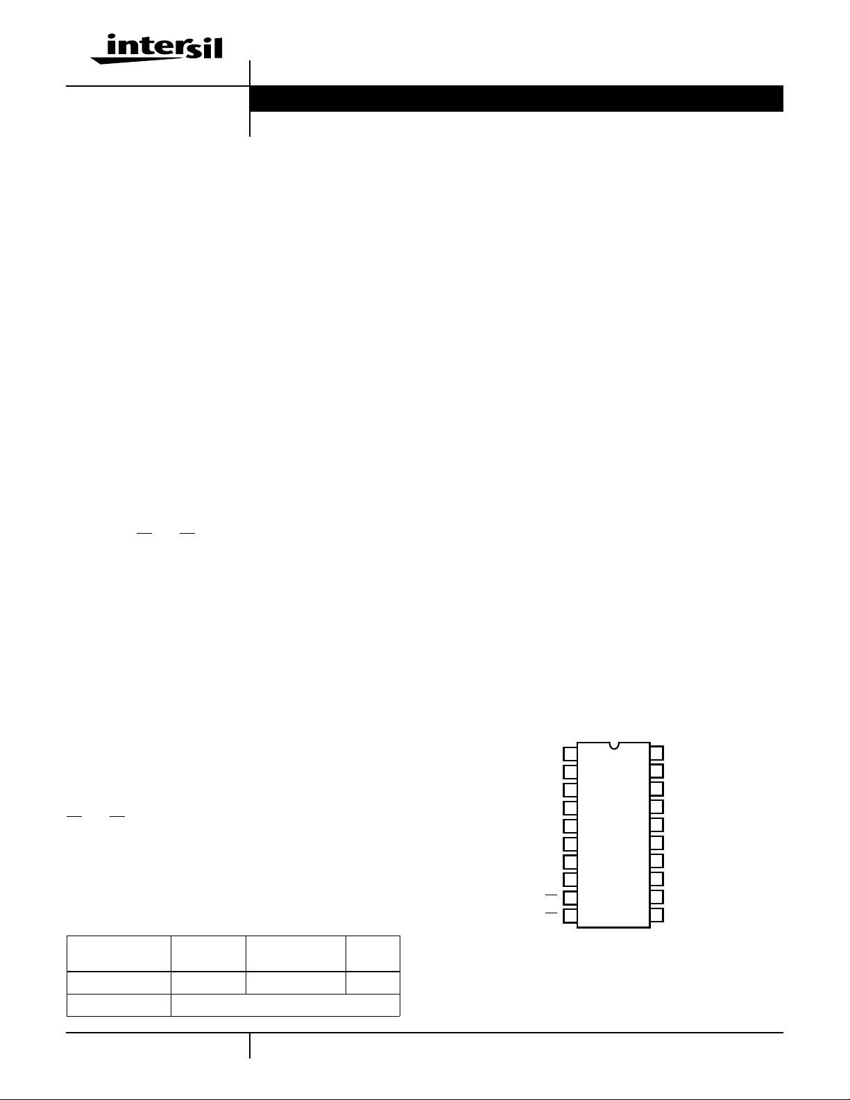
Pinout
HIP6502
(SOIC)
TOP VIEW
VSEN2
5VSB
VSEN1
3V3DLSB
3V3DL
VCLK
3V3
EN5VDL
S3
S5
1
2
3
4
5
6
7
8
9
10
20
19
18
17
16
15
14
13
12
11
MSEL
DRV2
5V
12V
SS
5VDL
5VDLSB
DLA
FAULT
GND
TEMP.
PART NUMBER
HIP6502CB 0 to 70 20 Ld SOIC M20.3
HIP6502EVAL1 Evaluation Board
RANGE (oC) PACKAGE
1
PKG.
NO.
CAUTION: These devices are sensitive to electrostatic discharge; follow proper IC Handling Procedures.
1-888-INTERSIL or 321-724-7143
| Copyright © Intersil Corporation 1999
Page 2
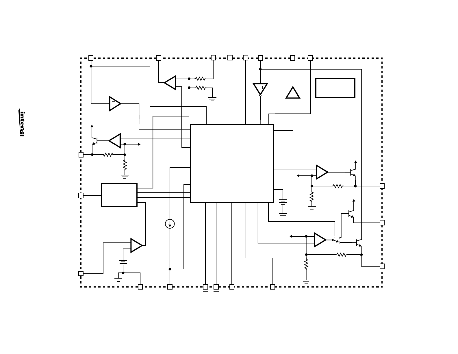
Block Diagram
12V
2
TO 5VSB
12V MONITOR
EA3
10.2V/9.2V
+
3V3DLSB
EA4
-
+
3V3DL
5V
3V3
5VSB
5VSB POR
4.5V/4.0V
5VDLSB
DLA
TEMPERATURE
MONITOR
(TMON)
-
TO UV
VSEN1
FAULT
UV DETECTOR
DETECTOR
MONITOR AND CONTROL
TO
UV DETECTOR
+
1.265V
-
TO 3V3
EA3
+
HIP6502
-
VCLK
TO 5V
5VDL
3.75V
-
+
UV COMPARATOR
+
-
GND
SS
10µA
S3
S5
EN5VDL
FIGURE 1.
MSEL
TO UV
DETECTOR
DRV2
EA2
-
+
VSEN2
Page 3

Simplified Power System Diagram
+5V
IN
+12V
IN
+5V
SB
+3.3V
IN
Q6
3.3V
MEM
3.3V
Q2
3.3V
DUAL
FAULT
MSEL
SHUTDOWN
SX
EN5VDL
/3.3V
3.3V
SB
Q3
2
Typical Application
HIP6502
LINEAR
REGULATOR
LINEAR
CONTROLLER
HIP6502
FIGURE 2.
LINEAR
CONTROLLER
LINEAR
REGULATOR
CONTROL
LOGIC
Q1
V
2.5V
V
2.5V
MEM
CLK
Q5
Q4
5V
DUAL
5V
+5V
IN
+12V
IN
+5V
SB
+3.3V
IN
V
OUT1
3.3V
3.3V
FAULT
SLP_S3
SLP_S5
EN5VDL
MSEL
SHUTDOWN
MEM
V
OUT3
DUAL
/3.3V
Q2
SB
Q6
C
OUT1
C
Q3
OUT3
VSEN1
5V
3V3DLSB
3V3DL
FAULT
S3
S5
EN5VDL
MSEL
SS
C
SS
12V
3V3
HIP6502
GND
5VSB
DRV2
VSEN2
C
OUT2
VCLK
5VDLSB
DLA
5VDL
C
OUT4
Q1
C
OUT5
Q5
Q4
V
2.5V
2.5V
V
5V
OUT2
V
OUT4
OUT5
DUAL
MEM
CLK
FIGURE 3.
3
Page 4

HIP6502
Absolute Maximum Ratings Thermal Information
Supply Voltage, V
12V. . . . . . . . . . . . . . . . . . . . . . . . . . . . . . . . . GND - 0.3V to +14.5V
DLA, DRV2. . . . . . . . . . . . . . . . . . . . . . . .GND - 0.3V to V
All Other Pins. . . . . . . . . . . . . . . . . . . . .GND - 0.3V to 5VSB + 0.3V
ESD Classification . . . . . . . . . . . . . . . . . . . . . . . . . . . . . . . . .Class 3
Recommended Operating Conditions
Supply Voltage, V
Digital Inputs, VSX,V
Ambient Temperature Range. . . . . . . . . . . . . . . . . . . . .0oC to 70oC
Junction Temperature Range. . . . . . . . . . . . . . . . . . . . 0oC to 125oC
CAUTION: Stresses above those listed in “Absolute Maximum Ratings” may cause permanent damage to the device. This is a stress only rating and operation of the
device at these or any other conditions above those indicated in the operational sections of this specification is not implied.
NOTE:
1. θJA is measured with the component mounted on an evaluation PC board in free air.
Electrical Specifications Recommended Operating Conditions, Unless Otherwise Noted Refer to Figures 1, 2 and 3
VCC SUPPLY CURRENT
Nominal Supply Current I
Shutdown Supply Current I
POWER-ON RESET, SOFT-START, AND VOLTAGE MONITORS
Rising 5VSB POR Threshold - - 4.5 V
5VSB POR Hysteresis - 0.2 - V
Rising 12V Threshold - - 10.2 V
12V Hysteresis - 1.0 - V
Rising 3V3 and 5V Thresholds -90- %
3V3 and 5V Hysteresis -5- %
Soft-Start Current I
Shutdown Voltage Threshold V
3.3V
Regulation - - 2.0 %
VSEN1 Nominal Voltage Level V
VSEN1 Undervoltage Rising Threshold - 2.77 - V
VSEN1 Undervoltage Hysteresis - 110 - mV
VSEN1 Output Current I
2.5V
Regulation - - 2.0 %
VSEN2 Nominal Voltage Level V
VSEN2 Undervoltage Rising Threshold - 2.075 - V
VSEN2 Output Current I
DRV2 Output Drive Current I
3.3V
Sleep State Regulation - - 2.0 %
3V3DL Nominal Voltage Level V
LINEAR REGULATOR (V
MEM
LINEAR REGULATOR (V
MEM
/3.3VSB LINEAR REGULATOR (V
DUAL
. . . . . . . . . . . . . . . . . . . . . . . . . . . . . . +7.0V
5VSB
Thermal Resistance (Typical, Note 1) θJA (oC/W)
SOIC Package. . . . . . . . . . . . . . . . . . . . . . . . . . . . . 85
+0.3V
12V
Maximum Junction Temperature (Plastic Package) . . . . . . . .150oC
Maximum Storage Temperature Range. . . . . . . . . . -65oC to 150oC
Maximum Lead Temperature (Soldering 10s) . . . . . . . . . . . . .300oC
(SOIC - Lead Tips Only)
. . . . . . . . . . . . . . . . . . . . . . . . . . . +5V ±5%
5VSB
EN5VDL
, V
. . . . . . . . . . . . . . 0 to +5.25V
MSEL
PARAMETER SYMBOL TEST CONDITIONS MIN TYP MAX UNITS
-30- mA
-10- µA
- - 0.8 V
- 3.3 - V
OUT1
OUT2
5VSB
5VSB(OFF)VSS
)
VSEN1
VSEN1
)
VSEN2
VSEN2
DRV2
)
OUT3
3V3DL
= 0.8V - 14 - mA
SS
SD
MSEL > 1.8V - 3.3 - V
5VSB = 5V 250 300 - mA
MSEL < 2.0V - 2.5 - V
5VSB = 5V 250 300 - mA
5VSB = 5V 220 - - mA
4
Page 5

HIP6502
Electrical Specifications Recommended Operating Conditions, Unless Otherwise Noted Refer to Figures 1, 2 and 3 (Continued)
PARAMETER SYMBOL TEST CONDITIONS MIN TYP MAX UNITS
3V3DL Undervoltage Rising Threshold - 2.77 - V
3V3DL Undervoltage Hysteresis - 110 - mV
3V3DLSB Output Drive Current I
3V3DLSB
DLA Output Impedance -90- Ω
2.5V
LINEAR REGULATOR (V
CLK
OUT4
)
Regulation - - 2.0 %
VCLK Nominal Voltage Level V
VCLK
VCLK Undervoltage Rising Threshold - 2.10 - V
VCLK Undervoltage Hysteresis -80- mV
VCLK Output Current (Note 2) I
5V
SWITCH CONTROLLER (V
DUAL
OUT5
VCLK
)
5VDL Undervoltage Rising Threshold - 4.22 - V
5VDL Undervoltage Hysteresis - 170 - mV
5VDLSB Output Drive Current I
5VDLSB
5VDLSB Pull-Up Impedance to 5VSB - 350 - Ω
TIMING INTERVALS
Active State Assessment Past Input UV
Thresholds (Note 3)
Active-to-Sleep Control Input Delay - 200 - µs
CONTROL I/O (S3, S5, EN5VDL, MSEL, FAULT)
High Level Input Threshold - - 2.2 V
Low Level Input Threshold 0.8 - - V
S3, S5 Internal Pull-up Impedance to 5VSB - 70 - kΩ
FAULT Output Impedance FAULT = high - 100 - Ω
TEMPERATURE MONITOR
Fault-Level Threshold (Note 4) 140 - Shutdown-Level Threshold (Note 4) - 155 -
NOTES:
2. At Ambient Temperatures Less Than 50oC.
3. Guaranteed by Correlation.
4. Guaranteed by Design.
5VSB = 5V 5 8.5 - mA
- 2.5 - V
V
= 3.3V 500 800 - mA
3V3
5VDLSB = 4V, 5VSB = 5V -20 - -40 mA
20 25 30 ms
o
o
C
C
5
Page 6

HIP6502
Functional Pin Description
3V3 (Pin 7)
Connect this pin to the ATX 3.3V output. This pin provides
the output current for the 2V5CLK pin, and is monitored for
power quality.
5VSB (Pin 2)
Provide a very well de-coupled 5V bias supply for the IC to
this pin by connecting it to the ATX 5VSB output. This pin
provides the output current for the VSEN1 and VSEN2 pins,
as well as the base current for Q2. The voltage at this pin is
monitored for power-on reset (POR) purposes.
5V (Pin 18)
Connect this pin to the ATX 5V output. This pin provides the
base bias current for Q1, and is monitored for power quality.
12V (Pin 17)
Connect this pin to the ATX 12V output. This pin provides the
gate bias voltage for Q3, Q5 and Q6, and is monitored for
power quality.
GND (Pin 11)
Signal ground for the IC. All voltage levels are measured with
respect to this pin.
S3 and S5 (Pins 9 and 10)
These pins switch the IC’s operating state from active (S0,
S1/S2) to S3 and S4/S5 sleep states. These are digital
inputs featuring internal 50kΩ (typical) resistor pull-ups to
5VSB. Internal circuitry de-glitches these pins for
disturbances lasting as long as 2µs (typically). Additional
circuitry blocks any illegal state transitions (such as S3 to
S4/S5 or vice versa). Respectively, connect
computer system’s
SLP_S3 and SLP_S5 signals.
MSEL (Pin 20)
Unconnected, this pin is held at approximately 1.9V by an
internal resistor divider. Pulling this pin below 0.9V enables
the 2.5V
above 2.9V enables the 3.3V
levels) and disables 2.5V output. Leaving the pin open
enables both memory regulators.
output and disables 3.3V
MEM
output (typical voltage
MEM
EN5VDL (Pin 8)
This pin enables or disables sleep state support on the
5V
is a digital input pin whose status can only be changed
during active state operation or during chip shutdown (SS
pin grounded by external open-drain device or chip bias
below POR level). The input information is latched-in when
entering a sleep state, as well as following 5VSB POR
release or exit from shutdown. EN5VDL is internally pulled
high through a 40µA current source.
output in response to S3 and S4/S5 requests. This
DUAL
S3 and S5 to the
output. Pulling it
MEM
FAULT (Pin 12)
In case of an undervoltage on any of the outputs or on any of
the monitored ATX outputs, or in case of an overtemperature
event, this pin is used to report the fault condition by being
pulled to 5VSB.
SS (Pin 16)
Connect this pin to a small ceramic capacitor (no less than
5nF; 0.1µF recommended). The internal soft-start (SS)
current source along with the external capacitor creates a
voltage ramp used to control the ramp-up of the output
voltages.Pulling this pin low with an open-drain device shuts
down all the outputs as well as forces the FAULTpin low.The
C
capacitor is also used to provide a controlled voltage
SS
slew rate during active-to-sleep transitions on the 3.3V
and V
MEM
outputs.
DUAL
VSEN2 (Pin 1)
Connect this pin to the 2.5V memory output (V
sleep states, this pin is regulated to 2.5V through an internal
pass transistor capable of delivering 300mA (typically). The
active-state voltage at this pin is regulated through an
external NPN transistor connected at the DRV2 pin. During
all operating states, the voltage at this pin is monitored for
under-voltage events.
OUT2
). In
DRV2 (Pin 19)
Connect this pin to the base of a suitable NPN transistor.
This pass transistor regulates the 2.5V output from the ATX
3.3V during active states operation.
3V3DL (Pin 5)
Connect this pin to the 3.3V dual/stand-by output (V
In sleep states, the voltage at this pin is regulated to 3.3V;in
active states, ATX 3.3V output is delivered to this node
through a fully on N-MOS transistor. During all operating
states, this pin is monitored for under-voltage events.
OUT3
).
3V3DLSB (Pin 4)
Connect this pin to the base of a suitable NPN transistor. In
sleep state, this transistor is used to regulate the voltage at
the 3V3DL pin to 3.3V.
DLA (Pin 13)
Connect this pin to the gates of suitable N-MOSFETs, which
in active state, switch in the ATX 3.3V and 5V outputs into
the 3.3V
respectively.
MEM
, 3.3V
/3.3VSB and 5V
DUAL
DUAL
outputs,
5VDL (Pin 15)
Connect this pin to the 5V
operating state, the voltage at this pin is provided through a
fully on MOS transistor. This pin is also monitored for undervoltage events.
DUAL
output (V
OUT5
). In either
,
6
Page 7

HIP6502
5VDLSB (Pin 14)
Connect this pin to the gate of a suitable P-MOSFET or
bipolar PNP. In sleep state, this transistor is switched on,
connecting the ATX 5VSB output to the 5V
DUAL
regulator
output.
VSEN1 (Pin 3)
Connect this pin to the 3.3V memory output (V
sleep states, this pin is regulated to 3.3V through an internal
pass transistor capable of delivering 300mA (typically). The
active-state voltage at this pin is provided from the ATX3.3V
through a fully on external N-MOS transistor. During all
operating states, the voltage at this pin is monitored for
under-voltage events.
OUT1
). In
VCLK (Pin 6)
This pin is the output of the internal 2.5V clock chip regulator
(V
). This internal regulator operates only in active
OUT4
states (S0, S1/S2) and is shut off during any sleep state,
regardless of the configuration of the chip. This pin is
monitored for under-voltage events.
Description
Operation
The HIP6502 controls 5 output voltages (Refer to Figures 1,
2, and 3). It is designed for microprocessor computer
applications with 3.3V, 5V, 5VSB, and 12V bias input from an
ATX power supply. The IC is composed of three linear
controllers/regulators supplying the computer system’s
3.3V
and PCI slots’ 3.3V
SB
RDRAM and 3.3V SDRAM memory power (V
an integrated regulator dedicated to 2.5V clock chip
(V
voltage (V
), a dual switch controller supplying the 5V
OUT4
), as well as all the control and monitoring
OUT5
functions necessary for complete ACPI implementation.
Initialization
The HIP6502 automatically initializes upon receipt of input
power. The Power-On Reset (POR) function continually
monitors the 5VSB input supply voltage, initiating 3.3V
soft-start operation after exceeding POR threshold. At 3ms
(typically) after 3.3V
status is latched in and the chip proceeds to ramp up the
remainder of the voltages, as required.
finishes its ramp-up, the EN5VDL
SB
AUX
power (V
), the 2.5V
OUT3
OUT2,VOUT1
DUAL
SB
Additionally, the internal circuitry does not allow the
transition from an S3 (suspend to RAM) state to an S4/S5
(suspend to disk/soft off) state or vice versa. The only ‘legal’
transitions are from an active state (S0, S1) to a sleep state
(S3, S5) and vice versa.
TABLE 1. 5V
EN5VDL S5 S3 5VDL COMMENTS
0 1 1 5V S0, S1 States (Active)
0100VS3
0 0 1 Note Maintains Previous State
0 0 0 0V S4/S5
1 1 1 5V S0, S1 States (Active)
1105VS3
1 0 1 Note Maintains Previous State
1 0 0 5V S4/S5
NOTE: Combination Not Allowed.
DUAL
OUTPUT (V
) TRUTH TABLE
OUT5
Functional Timing Diagrams
Figures 4 through 6 are timing diagrams, detailing the power
up/down sequences of all three outputs in response to the
status of the enable (EN5VDL) and sleep-state pins (
S5), as well as the status of the ATX supply.
5VSB
S3
),
S5
3.3V,
5V, 12V
3V3DLSB
DLA
3V3DL
5VDLSB
5VDL
FIGURE 4. 5V
3.3V
TIMING DIAGRAM FOR EN5VDL = 1;
DUAL
/3.3V
DUAL
SB
S3,
Operational Truth Table
The EN5VDL pin offers the choice of supporting or disabling
5VDUAL output in S3 and S4/S5 sleep states. Table 1
describes the truth combinations pertaining to this output.
Not shown in any of the tables are the 3.3V
the 2.5V
outputs. The 3.3V
CLK
/3.3VSB output powers
DUAL
up as soon as the 5VSB ATX output is available. The
2.5V
output operation is restricted by the chip’s POR and
CLK
is only available in active state (S0, S1). For additional
information, see the soft-start sequence diagrams.
7
DUAL
/3.3VSBand
The status of the EN5VDL pin can only be changed while in
active (S0, S1) states, when the bias supply (5VSB pin) is
below POR level, or during chip shutdown (SS pin shorted to
GND or within 3ms of 5VSB POR); a status change of this
pin while in a sleep state is ignored.
Page 8

5VSB
S3
S5
3.3V,
5V, 12V
3V3DLSB
DLA
3V3DL
HIP6502
proportional to the SS (soft-start) pin voltage. As the SS pin
voltage slews from about 1.25V to 2.5V, the input clamp
allows a rapid and controlled output voltage rise.
5VSB
(1V/DIV)
SOFT-START
(1V/DIV)
5VDLSB
5VDL
FIGURE 5. 5V
3V
TIMING DIAGRAM FOR EN5VDL = 0;
DUAL
/3V
DUAL
SB
Not shown in these diagrams is the deglitching feature used
to protect against false sleep state tripping. Both
S3 and S5
pins are protected against noise by a 2µs filter (typically 1 4µs). This feature is useful in noisy computer environments if
the control signals have to travel over significant distances.
Additionally, the
transitioning to sleep states. Once the
S3 pin features a 200µs delay in
S3 pin goes low, an
internal timer is activated. At the end of the 200µs interval, if
the
S5 pin is low, the HIP6502 switches into S5 sleep state; if
the
S5 pin is high, the HIP6502 goes into S3 sleep state.
5VSB
S3
S5
3.3V,
5V, 12V
INTERNAL
VSEN1, 2
DEVICES
DRV2
VSEN2
DLA
VSEN1
VCLK
FIGURE 6. 2.5V
MEM
, 3.3V
MEM
, AND 2.5V
CLK
TIMING
DIAGRAM; MSEL FLOATING (NOT CONNECTED)
Soft-Start Circuit
SOFT-START INTO SLEEP STATES (S3, S4/S5)
The 5VSB POR function initiates the soft-start sequence. An
internal 10µA current source charges an external capacitor.
The error amplifiers reference inputs are clamped to a level
0V
V
0V
OUTPUT
VOLTAGES
(1V/DIV)
T1 T2
T0
V
OUT3
(3.3V
T3
DUAL
/3.3VSB)
TIME
T5T4
OUT5
V
OUT1
V
(2.5V
(5V
OUT2
MEM
DUAL
(3.3V
)
MEM
V
(2.5V
)
)
OUT4
CLK
)
FIGURE 7. SOFT-START INTERVAL IN A SLEEP STATE
(ALL OUTPUTS ENABLED)
Figure 7 shows the soft-start sequence for the typical
application start-up in sleep state with all output voltages
enabled. At time T0 5VSB (bias) is applied to the circuit. At
time T1 the 5VSB surpasses POR level. An internal fast
charge circuit quickly raises the SS capacitor voltage to
approximately 1V, then the 10µA current source continues
the charging. The soft-start capacitor voltage reaches
approximately 1.25V at time T2, at which point the
3.3V
/3.3VSB error amplifier’s reference input starts its
DUAL
transition, causing the output voltage to ramp up
proportionally.The ramp-up continues until time T3 when the
3.3V
/3.3VSB voltage reaches the set value. After this
DUAL
output reached its set value, as the soft-start capacitor
voltage reaches approximately 2.75V, the under-voltage
monitoring circuit of this output is activated and the soft-start
capacitor is quickly discharged to approximately 1.25V.
Following the 3ms (typical) time-out between T3 and T4, the
MSEL and EN5VDL selections are latched in, and the softstart capacitor commences a second ramp-up designed to
smoothly bring up the remainder of the voltages required by
the system. At time T5 all voltages are within regulation
limits, and as the SS voltage reaches 2.75V, all the
remaining UV monitors are activated and the SS capacitor is
quickly discharged to 1.25V, where it remains until the next
transition.
8
Page 9

HIP6502
SOFT-START INTO ACTIVE STATES (S0, S1)
S3 and S5 are logic high at the time the 5VSB is
If both
applied, the HIP6502 will assume active state wake-up and
keep off the controlled external transistors and the VCLK
output until some time (typically 25ms) after the ATX’s main
outputs used by the application (3.3V, 5V, and 12V) exceed
the set thresholds. This time-out feature is necessary in
order to insure the main ATX outputs are stabilized. The
time-out also assures smooth transitions from sleep into
active when sleep states are being supported.
3.3V
/3.3VSB output, whose operation is only
DUAL
dependent on 5VSB presence, will come up right as bias
voltage reaches POR level.
+12V
+5VSB
0V
INPUT VOLTAGES
(2V/DIV)
+5V
+3.3V
OUTPUT
VOLTAGES
(1V/DIV)
IN
IN
IN
V
OUT5
DLA PIN
(2V/DIV)
SOFT-START
(5V
DUAL
(1V/DIV)
)
are ramped-up, reaching regulation limits at time T3.
Simultaneous with the beginning of the memory and clock
voltage ramp-up, at time T2, the DLA pin is pulled high,
turning on Q3, Q5, and Q6 in the process, and bringing the
3.3V
MEM
and 5V
outputs in regulation. Shortly after
DUAL
time T3, as the SS voltage reaches 2.75V, the soft-start
capacitor is quickly discharged down to approximately2.45V,
where it remains until a valid sleep state request is received
from the system.
It is important to note that in the typical application (as
pictured in Figure 3) the 3.3V memory output is powered up
during active state operation, regardless of the MSEL pin
status. Sleep state support on this output is, however,
dependent on the MSEL status.
Fault Protection
All the outputs are monitored against undervoltage events. A
severe overcurrent caused by a failed load on any of the
outputs, would, in turn, cause that specific output to
suddenly drop. If any of the output voltages drop below 80%
(typical) of their set value, such event is reported by having
the FAULT pin pulled to 5V. Additionally, exceeding the
maximum current rating of an integrated regulator (output
with pass regulator on chip) can lead to output voltage
drooping; if excessive, this droop can ultimately trip the
under-voltage detector and send a FAULT signal to the
computer system.
V
(
3.3V
OUT1
V
(3.3V
OUT3
0V
T1 T2
T0
FIGURE 8. SOFT-START INTERVALIN ACTIVE STATE
(2.5/3.3V
/3.3VSB)
DUAL
)
MEM
TIME
OUTPUT SHOWN IN 2.5V SETTING)
MEM
(2.5V
T3
V
OUT2, 4
MEM
, 2.5V
CLK
)
During sleep to active state transitions from conditions
where the outputs are initially 0V (such as S5 to S0 transition
on the 5V
sequence directly into active state), the 3.3V
5V
DUAL
output with EN5VDL = 0, or simple power-up
DUAL
MEM
and
outputs go through a quasi soft-start by being pulled
high through the body diodes of the N-Channel MOSFETs
connected between these outputs and the 3.3V and 5V ATX
outputs. Figure 8 shows this start-up.
5VSB is already present when the main ATX outputs are
turned on at time T0. As a result of +3.3V
ramping up, the 3.3V
MEM
and 5V
DUAL
and +5V
IN
IN
output capacitors
charge up through the body diodes of Q6 and Q5,
respectively (see Figure 3). At time T1, all main ATX outputs
exceed the HIP6502’s undervoltage thresholds, and the
internal 25ms (typical) timer is initiated. At T2 the time-out
initiates a soft-start, and the 2.5V memory and clock outputs
A FAULT condition occurring on an output when controlled
through an external pass transistor will only set off the
FAULT flag, and it will not shut off or latch off any part of the
circuit. A FAULT condition occurring on an output when
controlled through an internal pass transistor, will set off the
FAULT flag, and it will shut off the faulting regulator only. If
shutdown or latch off of the entire circuit is desired in case of
a fault, regardless of the cause, this can be achieved by
externally pulling or latching the SS pin low. Pulling the SS
pin low will also force the FAULT pin to go low and reset an
internally latched-off output.
Special consideration is given to the initial start-up
sequence. If, following a 5VSB POR event, the
3.3V
/3.3VSB output is ramped up and is subject to an
DUAL
undervoltage event before the remainder of the controlled
voltages have been brought up, then the FAULT output goes
high and the entire IC latches off. Latch-off condition can be
reset by cycling the bias power (5VSB). Undervoltage events
on the 3.3V
/3.3VSB output at any other times are
DUAL
handled according to the description found in the second
paragraph under the current heading.
Another condition that could set off the FAULT flag is chip
over-temperature. If the HIP6502 reaches an internal
temperature of 140
o
C (typical), the FAULT flag is set off, but
the chip continues to operate until the temperature reaches
o
155
C (typical), when unconditional shutdown of all outputs
takes place. Operation resumes at 140
o
C and the
9
Page 10

HIP6502
temperature cycling occurs until the fault-causing condition
is removed.
Output Voltages
The output voltages are internally set and do not require any
external components. Selection of the memory voltages is
done by means of the MSEL pin. Leaving the MSEL pin
floating enables support of both memory outputs. Pulling the
MSEL pin below 0.9V enables support only for the 2.5V
MEM
output. It is important to notice that in a typical application
(such as that presented in Figure 3), setting the MSEL low
will not prevent the 3.3V
state. Pulling the MSEL pin above 2.9V enables 3.3V
from being operational in active
MEM
MEM
output support, only. Following every 3.3VSB ramp-up, chip
reset (see Soft-Start Circuit), or at the exit from an S4/S5
sleep state, the MSEL setting is latched in. During active
state (S0/S1/S2) and S3 sleep state, any changes in MSEL
status are ignored.
Application Guidelines
Soft-Start Interval
The 5VSB output of a typical ATX supply is capable of
725mA. During power-up in a sleep state, it needs to provide
sufficient current to charge up all the output capacitors and
simultaneously provide some amount of current to the output
loads. Drawing excessive amounts of current from the 5VSB
output of the ATX can lead to voltage collapse and induce a
pattern of consecutive restarts with unknown effects on the
system’s behavior or health.
The built-in soft-start circuitry allows tight control of the slewup speed of the output voltages controlled by the HIP6502,
thus enabling power-ups free of supply drop-off events.
Since the outputs are ramped up in a linear fashion, the
current dedicated to charging the output capacitors can be
calculated with the following formula:
I
SS
I
COUT
I
SS
------------------------------
CSSVBG×
Σ C
OUTVOUT
×()×=
- soft-start current (typically 10µA)
CSS - soft-start capacitor
VBG - bandgap voltage (typically 1.26V)
Σ(C
OUT
x V
) - sum of the products between the
OUT
capacitance and the voltage of an output (total charge
delivered to all outputs)
Due to the various system timing events, it is recommended
that the soft-start interval not be set to exceed 30ms.
Shutdown
In case of a FAULT condition that might endanger the
computer system, or at any other time, all the HIP6502
outputs can be shut down by pulling the SS pin below the
specified shutdown level (typically 0.8V) with an open drain
or open collector device capable of sinking a minimum of
2mA. Pulling the SS pin low effectively shuts down all the
, where
pass elements. Upon release of the SS pin, the HIP6502
undergoes a new soft-start cycle and resumes normal
operation in accordance to the ATX supply and control pins
status.
Layout Considerations
The typical application employing a HIP6502 is a fairly
straight forward implementation. Like with any other linear
regulator, attention has to be paid to the few potentially
sensitive small signal components, such as those connected
to sensitive nodes or those supplying critical by-pass
current.
The power components (pass transistors) and the controller
IC should be placed first. The controller should be placed in
a central position on the motherboard, closer to the memory
load if possible, but not excessivelyfar from the clock chip or
the processor. Insure the VSEN1 and VSEN2 connections
are properly sized to carry 250mA without significant
resistive losses; similar guideline applies to the VCLK
output, which can deliver as much as 800mA (typical). As
the current for the VCLK output is provided from the ATX
3.3V, the connection from the 3V3 pin to the 3.3V plane
should be sized to carry the maximum clock output current
while exhibiting negligiblevoltage losses. Similarly,the 5VSB
pin and the 5V pin are carrying significant levels of current for best results, insure these pins are connected to their
respective sources through adequate traces. The pass
transistors should be placed on pads capable of heatsinking
matching the device’s power dissipation. Where applicable,
multiple via connections to a large internal plane can
significantly lower localized device temperature rise.
Placement of the decoupling and bulk capacitors should
follow a placement reflecting their purpose. As such, the
high-frequency decoupling capacitors should be placed as
close as possible to the load they are decoupling; the ones
decoupling the controller close to the controller pins, the
ones decoupling the load close to the load connector or the
load itself (if embedded). Even though bulk capacitance
(aluminum electrolytics or tantalum capacitors) placement is
not as critical as the high-frequency capacitor placement,
having these capacitors close to the load they serve is
preferable.
The only critical small signal component is the soft-start
capacitor,C
control IC and connect to ground through a via placed close
to the capacitor’s ground pad. Minimize any leakage current
paths from SS node, since the internal current source is only
10µA.
. Locate this component close to SS pin of the
SS
10
Page 11

HIP6502
+12V
IN
+5V
SB
C
BULK5
Q1
IN
V
C
V
OUT2
BULK2
OUT5
C
HF5
Q5
+5V
+3.3V
Q4
IN
C
HF2
LOAD
IN
C
LOAD
C
C
HF1
V
OUT1
LOAD
BULK4
HF4
Q3
C
V
LOAD
HF3
OUT3
C
Q2
5VSB
5VDLSB
5VDL
C
5VSB
BULK1
C
12V
12V
C
SS
SS
VSEN1
3V3DLSB
HIP6502
3V3DL
C
BULK3
VCLK
3V3
Q6
KEY
ISLAND ON POWER PLANE LAYER
ISLAND ON CIRCUIT/POWER PLANE LAYER
VIA CONNECTION TO GROUND PLANE
GND
DLA
5V
VSEN2
DRV2
C
FIGURE 9. PRINTED CIRCUIT BOARD ISLANDS
A multi-layer printed circuit board is recommended. Figure 9
shows the connections of most of the components in the
converter. Note that the individual capacitors shown each
could represent numerous physical capacitors. Dedicate one
solid layer for a ground plane and make all critical
component ground connections through vias placed as close
to the component terminal as possible. Dedicate another
solid layer as a power plane and break this plane into
smaller islands of common voltage levels. Ideally, the power
plane should support both the input power and output power
nodes. Use copper filled polygons on the top and bottom
circuit layers to create power islands connecting the filtering
components (output capacitors) and the loads. Use the
remaining printed circuit layers for small signal wiring.
Component Selection Guidelines
LOAD
transient load regulation, paying attention to their parasitic
components (ESR, ESL).
Also, during the transition between active and sleep states,
there is a short interval of time during which none of the
power pass elements are conducting - during this time the
output capacitors have to supply all the output current. The
output voltage drop during this brief period of time can be
easily approximated with the following formula:
V
∆ I
OUT
∆V
- output voltage drop
OUT
ESR
I
OUT
C
- output capacitor bank ESR
OUT
- output current during transition
- output capacitor bank capacitance
OUT
ESR
×=
OUT
OUT
--------------- -+
C
t
t
OUT
, where
tt - active-to-sleep or sleep-to-active transition time (10µs typ.)
The output voltage drop is heavily dependent on the ESR
(equivalent series resistance) of the output capacitor bank,
the choice of capacitors should be such as to maintain the
output voltage above the lowest allowable regulation level.
V
(V
CLK
The output capacitor for the V
) Output Capacitors Selection
OUT4
linear regulator provides
CLK
loop stability. Figure 10 outlines a capacitance vs. equivalent
series resistance envelope. For stable operation and
optimized performance, select a C
OUT4
capacitor or
combination of capacitors with characteristics within the
shown envelope.
10
1
ESR (Ω)
0.1
0.01
10
100
CAPACITANCE (µF)
1000
Output Capacitors Selection
The output capacitors for all outputs should be selected to
allow the output voltage to meet the dynamic regulation
requirements of active state operation (S0, S1). The load
transient for the various microprocessor system’s
components may require high quality capacitors to supply
the high slew rate (di/dt) current demands. Thus, it is
recommended that the output capacitors be selected for
11
FIGURE 10. C
OUTPUT CAPACITOR
OUT4
Input Capacitors Selection
The input capacitors for an HIP6502 application have to
have a sufficiently low ESR as to not allow the input voltage
to dip excessively when energy is transferred to the output
capacitors. If the ATX supply does not meet the
specifications, certain imbalances between the ATX’s
outputs and the HIP6502’s regulation levels could have as a
Page 12

HIP6502
result a brisk transfer of energy from the input capacitors to
the supplied outputs. At the transition between active and
sleep states, this phenomena could result in the 5VSB
voltage dropping below the POR level (typically 4.1V) and
temporarily disabling the HIP6502. The solution to a
potential problem such as this is using larger input
capacitors with a lower total combined ESR.
Transistor Selection/Considerations
The HIP6502 usually requires one P-Channel (or bipolar
PNP), three N-Channel MOSFETs and two bipolar NPN
transistors.
One important criteria for selection of transistors for all the
linear regulators/switching elements is package selection for
efficient removal of heat. The power dissipated in a linear
regulator/switching element is
P
LINEARIOVINVOUT
–()×=
Select a package and heatsink that maintains the junction
temperature below the rating with the maximum expected
ambient temperature.
Q1
The active element on the 2.5V
bipolar NPN capable of conducting the maximum active
memory current and exhibit a current gain (h
40 at this current and 0.7V V
output has to be a
MEM
.
CE
) of minimum
fe
Q2
The NPN transistor used as sleep state pass element (Q2)
on the 3.3V
of 100 at 1.5V V
operating temperature range.
output has to have a minimum current gain
DUAL
and 500mA ICE throughout the in-circuit
CE
Q3, 4, 6
The three N-Channel MOSFETs are used to switch the 3.3V
and 5V inputs provided by the ATXsupply into the 3.3V
3.3V
/3.3VSB, and 5V
DUAL
outputs, while in active (S0,
DUAL
MEM
S1) state. The main criteria for the selection of these
transistors is output voltage budgeting. The maximum
r
allowed at highest junction temperature can be
DS(ON)
expressed with the following equation:
r
DS ON()max
V
- minimum input voltage
INmin
V
OUTmin
I
OUTmax
-------------------------------------------------- -=
- minimum output voltage allowed
- maximum output current
INminVOUTmin
I
OUTmax
, where
V
–
The gate bias availablefor these MOSFETs is of the order of
8V.
Q5
If a P-Channel MOSFET is used to switch the 5VSB output
of the ATX supply into the 5V
states (as dictated by EN5VDL status), then the selection
criteria of this device is proper voltage budgeting. The
maximum r
4.5V of V
GS
, however, has to be achieved with only
DS(ON)
, so a logic level MOSFET needs to be selected.
If a PNP device is chosen to perform this function, it has to
have a low saturation voltage while providing the maximum
sleep current and have a current gain sufficiently high to be
saturated using the minimum drive current (typically 20mA).
output during S3 and S5
DUAL
,
12
Page 13

HIP6502 Application Circuit
Figure 11 shows an application circuit of an ACPIsanctioned power management system fora microprocessor
computer system. The power supply provides the
3.3V
voltage (V
(V
OUT2
5V
+12VDC ATX supply outputs. Q4 can also be a PNP, such as
/3.3VSB voltage (V
DUAL
OUT1
), the 2.5V
voltage (V
DUAL
+5V
+12V
+3.3V
+5V
), the RDRAM 2.5V
OUT3
clock voltage (V
CLK
) from +3.3V, +5VSB, +5V, and
OUT5
IN
IN
IN
SB
C1
1µF
), the SDRAM 3.3V
memory voltage
MEM
OUT4
), and the
C3
1µF
MEM
HIP6502
12V
3V3
an MMBT2907AL. For detailed information on the circuit,
including a Bill-of-Materials and circuit board description,
see Application Note AN9862.
Also see Intersil Corporation’s web page
(http://www.intersil.com) or Intersil’s AnswerFAX
(407-724-7800) for the latest information.
+
C2
220µF
5VSB
C4
1µF
V
OUT1
3.3V
MEM
2SD1802
V
OUT3
3.3V
DUAL
CONFIGURATION
HARDWARE
SLP_S3
SLP_S5
HUF76113SK8
Q2
/3.3V
SB
1µF
Q6
C17
1µF
1/2 HUF76113DK8
C9
+
Q3
+
220µF
C10
C5,16
2X150µF
5V
VSEN1
3V3DLSB
3V3DL
FAULT
EN5VDL
MSEL
S3
S5
SS
U1
HIP6502
DRV2
VSEN2
VCLK
5VDLSB
DLA
5VDL
2X150µF
C11
150µF
C6,7
+
+
+
C14
150µF
Q1
2SD1802
C8
1µF
C12
1µF
Q5
1/2 HUF76113DK8
C15
1µF
V
2.5V
V
2.5V
Q4
FDV304P
V
5V
OUT2
MEM
OUT4
CLK
OUT5
DUAL
SHUTDOWN
(FROM OPEN-DRAIN N-MOS)
13
C13
0.1µF
GND
FIGURE 11. TYPICAL HIP6502 APPLICATION DIAGRAM
Page 14

Small Outline Plastic Packages (SOIC)
HIP6502
N
INDEX
AREA
123
-A-
E
-B-
SEATING PLANE
D
A
-C-
0.25(0.010) BM M
H
L
h x 45
o
α
e
B
0.25(0.010) C AM BS
M
NOTES:
1. Symbols are defined in the “MO Series Symbol List” in Section 2.2 of
Publication Number 95.
2. Dimensioning and tolerancing per ANSI Y14.5M-1982.
3. Dimension “D” does not include mold flash, protrusions or gate burrs.
Mold flash, protrusion and gate burrs shall not exceed 0.15mm (0.006
inch) per side.
4. Dimension“E” doesnotincludeinterlead flash orprotrusions.Interlead
flash and protrusions shall not exceed 0.25mm (0.010 inch) per side.
5. The chamfer on the body is optional. If it is not present, a visual index
feature must be located within the crosshatched area.
6. “L” is the length of terminal for soldering to a substrate.
7. “N” is the number of terminal positions.
8. Terminal numbers are shown for reference only.
9. The lead width “B”, as measured 0.36mm (0.014 inch) or greater
above the seating plane, shall not exceed a maximum value of
0.61mm (0.024 inch)
10. Controllingdimension: MILLIMETER. Converted inch dimensions
are not necessarily exact.
A1
C
0.10(0.004)
M20.3 (JEDEC MS-013-AC ISSUE C)
20 LEAD WIDE BODY SMALL OUTLINE PLASTIC PACKAGE
INCHES MILLIMETERS
SYMBOL
A 0.0926 0.1043 2.35 2.65 -
A1 0.0040 0.0118 0.10 0.30 -
B 0.013 0.0200 0.33 0.51 9
C 0.0091 0.0125 0.23 0.32 D 0.4961 0.5118 12.60 13.00 3
E 0.2914 0.2992 7.40 7.60 4
e 0.050 BSC 1.27 BSC H 0.394 0.419 10.00 10.65 h 0.010 0.029 0.25 0.75 5
L 0.016 0.050 0.40 1.27 6
N20 207
o
α
0
o
8
o
0
o
8
Rev. 0 12/93
NOTESMIN MAX MIN MAX
-
All Intersil semiconductor products are manufactured, assembled and tested under ISO9000 quality systems certification.
Intersil semiconductor products are sold by description only. Intersil Corporation reserves the right to make changes in circuit design and/or specifications at any time without notice. Accordingly, the reader is cautioned to verify that data sheets are current before placing orders. Information furnished by Intersil is believed to be accurate and
reliable. However, no responsibility is assumed by Intersil or its subsidiaries for its use; nor for any infringements of patents or other rights of third parties which may result
from its use. No license is granted by implication or otherwise under any patent or patent rights of Intersil or its subsidiaries.
For information regarding Intersil Corporation and its products, see web site www.intersil.com
Sales Office Headquarters
NORTH AMERICA
Intersil Corporation
P. O. Box 883, Mail Stop 53-204
Melbourne, FL 32902
TEL: (321) 724-7000
FAX: (321) 724-7240
14
EUROPE
Intersil SA
Mercure Center
100, Rue de la Fusee
1130 Brussels, Belgium
TEL: (32) 2.724.2111
FAX: (32) 2.724.22.05
ASIA
Intersil (Taiwan) Ltd.
7F-6, No. 101 Fu Hsing North Road
Taipei, Taiwan
Republic of China
TEL: (886) 2 2716 9310
FAX: (886) 2 2715 3029
 Loading...