Intersil Corporation HIP6501A Datasheet
HIP6501A
Data Sheet February 2000
Triple Linear Power Controller with ACPI
Control Interface
The HIP6501A, paired with either the HIP6020 or HIP6021,
simplifies the implementation of ACPI-compliant designs in
microprocessor and computer applications. The IC
integrates two linear controllers and a low-current pass
transistor, as well as the monitoring and control functions
into a 16-pin SOIC package. One linear controller generates
the 3.3V
5VSB output during sleep states (S3, S4/S5), powering the
PCI slots through an external pass transistor, as instructed
by thestatusofthe 3.3V
transistor is used to switch in the ATX 3.3V output for PCI
operation during S0 and S1 (active) operatingstates. The
second linear controller supplies the computer system’s
2.5V/3.3V memory power through an external pass
transistor in active states. During S3 state, an integrated
pass transistor supplies the 2.5V/3.3V sleep-state power. A
third controller powers up a 5V
the ATX 5V output in active states, or the ATX5VSB in sleep
states.
The HIP6501A’s operating mode (active-state outputs or
sleep-state outputs) is selectable through two control pins:
S3 and S5. Further control of the logic governing activation
of different power modes is offered through two enabling
pins:
EN3VDL and EN5VDL. In active states, the 3.3V
linear regulator uses an external N-Channel pass MOSFET
to connect the output (V
supplied by an ATX (or equivalent) power supply, while
incurring minimal losses. In sleep state, the 3.3V
is supplied from the ATX 5VSB through an NPN transistor,
also external to the controller. Active state power delivery for
the 2.5/3.3V
transistor, or an NMOS switch for the 3.3V setting. In sleep
states, conduction on this output is transferred to an internal
pass transistor. The 5V
external MOS transistors. In sleep states, a PMOS (or PNP)
transistor conducts the current from the ATX 5VSB output,
while in active states, current flow is transferred to an NMOS
transistor connected to the ATX 5V output. Similar to the
3.3V
DUAL
dictated not only by the status of the
of the EN5VDL pin as well.
voltage plane from an ATX power supply’s
DUAL
enable pin. An additional pass
DUAL
plane by switching in
DUAL
) directly to the 3.3V input
OUT1
output is done through an external NPN
MEM
output is powered through two
DUAL
output, the operation of the 5V
DUAL
S3 and S5 pins, but that
output
DUAL
output is
DUAL
File Number 4749.2
Features
• Provides 3 ACPI-Controlled Voltages
- 5V Active/Sleep (5V
- 3.3V Active/Sleep (3.3V
- 2.5V/3.3V Active/Sleep (2.5V
DUAL
)
DUAL
)
MEM
)
• Simple Control Design - No Compensation Required
• Excellent Output Voltage Regulation
- 3.3V
Output: ±2.0% Over Temperature; Sleep
DUAL
States Only
- 2.5V/3.3V Output: ±2.0% Over Temperature; Both
Operational States (3.3V setting in sleep only)
• Fixed Output Voltages Require No Precision External
Resistors
• Small Size
- Small External Component Count
• Selectable 2.5V
Output Voltage Via FAULT/MSEL Pin
MEM
- 2.5V for RDRAM Memory
- 3.3V for SDRAM Memory
• Under-Voltage Monitoring of All Outputs with Centralized
FAULT Reporting
• Adjustable Soft-Start Function Eliminates 5VSB
Perturbations
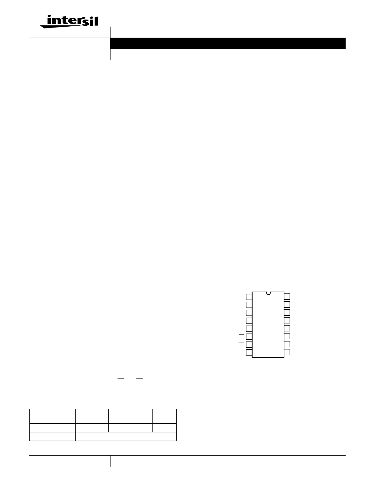
Pinout
HIP6501A (SOIC)
TOP VIEW
5VSB
EN3VDL
3V3DLSB
3V3DL
EN5VDL
S3
S5
GND
1
2
3
4
5
6
7
8
16
VSEN2
15
DRV2
14
12V
13
SS
12
5VDL
5VDLSB
11
DLA
10
9
FAULT/MSEL
Ordering Information
TEMP.
PART NUMBER
HIP6501ACB 0 to 70 16 Ld SOIC M16.15
HIP6501EVAL1 Evaluation Board
RANGE (oC) PACKAGE
1
PKG.
NO.
CAUTION: These devices are sensitive to electrostatic discharge; follow proper IC Handling Procedures.
1-888-INTERSIL or 321-724-7143 | Copyright © Intersil Corporation 2000
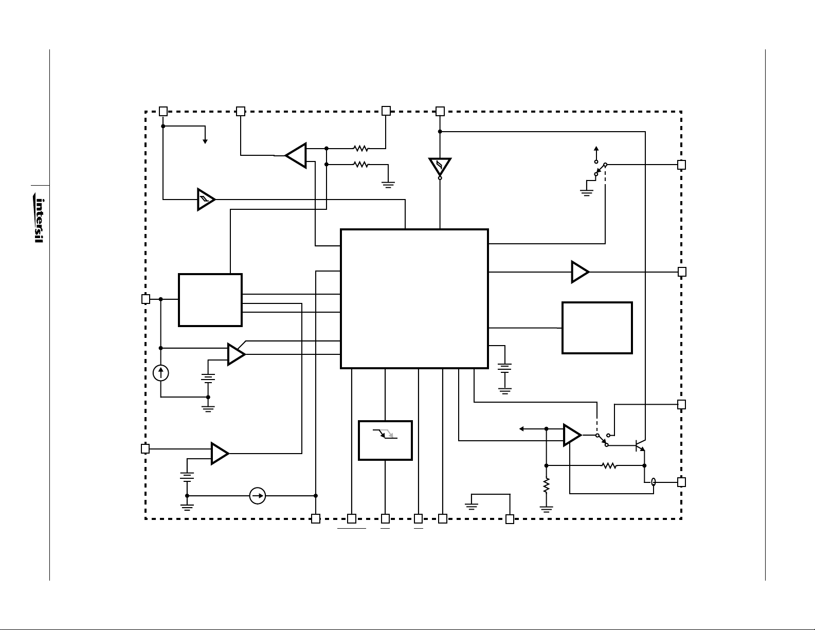
Block Diagram
12V
12V BIAS
2
12V MONITOR
10.8V/9.0V
3V3DLSB
EA4
+
3V3DL
5VSB
5VSB POR
4.5V/4.0V
TO 12V
DLA
5VDLSB
HIP6501A
FAULT/MSEL
UV DETECTOR
40µA
+
-
+
0.2V
MEM VOLTAGE
SELECT COMP
MONITOR AND CONTROL
TEMPERATURE
MONITOR
(TMON)
+
1.265V
-
5VDL
UV COMPARATOR
+
+
3.75V
-
10µA
SS
EN3VDL
DELAY
S3
FIGURE 1.
S5
EN5VDL
TO
UV DETECTOR
GND
EA2
DRV2
+
VSEN2
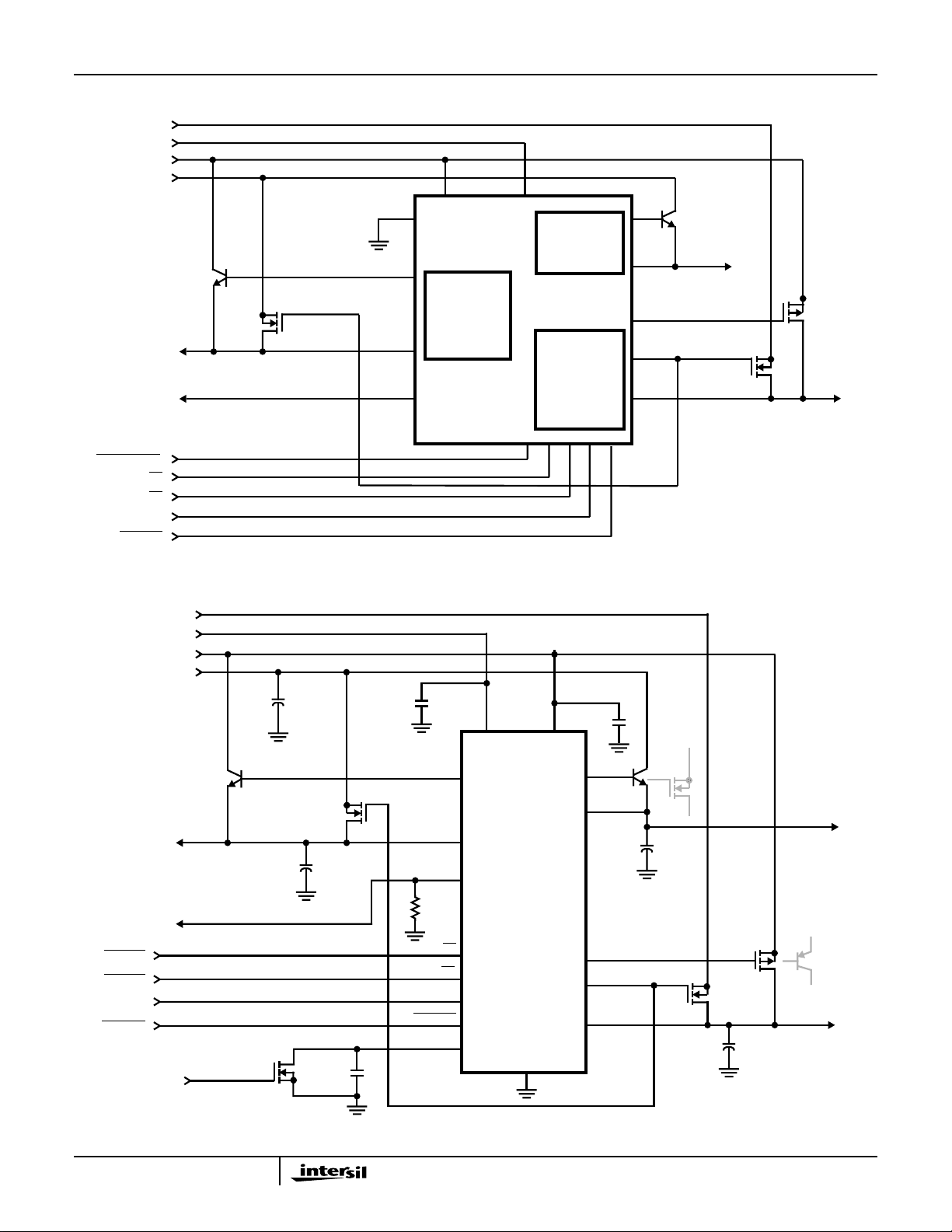
Simplified Power System Diagram
+5V
IN
+12V
IN
+5V
SB
+3.3V
IN
HIP6501A
Q2
3.3V
DUAL
FAULT
SHUTDOWN
S3
S5
EN5VDL
EN3VDL
Typical Application
+5V
IN
+12V
IN
+5V
SB
+3.3V
IN
Q3
LINEAR
CONTROLLER
FIGURE 2.
LINEAR
CONTROLLER
HIP6501A
CONTROL
LOGIC
Q1
2.5V
MEM
Q5
Q4
5V
DUAL
FAULT
SLP_S3
SLP_S5
EN5VDL
EN3VDL
SHUTDOWN
3.3V
V
OUT1
DUAL
Q2
Q3
C
C
OUT1
SS
3V3DLSB
3V3DL
FAULT/MSEL
R
SEL
S3
S5
EN5VDL
EN3VDL
SS
12V
HIP6501A
GND
5VSB
DRV2
VSEN2
C
OUT2
5VDLSB
DLA
5VDL
Q1
C
OUT3
Q5
2.5/3.3V
Q4
V
V
5V
OUT2
MEM
OUT3
DUAL
FIGURE 3.
3
HIP6501A
Absolute Maximum Ratings Thermal Information
Supply Voltage, V
12V. . . . . . . . . . . . . . . . . . . . . . . . . . . . . . . . . GND - 0.3V to +14.5V
DLA, DRV2. . . . . . . . . . . . . . . . . . . . . . . .GND - 0.3V to V
All Other Pins. . . . . . . . . . . . . . . . . . . . .GND - 0.3V to 5VSB + 0.3V
ESD Classification . . . . . . . . . . . . . . . . . . . . . . . . . . . . Class 3 [5kV]
Recommended Operating Conditions
Supply Voltage, V
Secondary Bias Voltage, V
Digital Inputs, V
Ambient Temperature Range. . . . . . . . . . . . . . . . . . . . .0oC to 70oC
Junction Temperature Range. . . . . . . . . . . . . . . . . . . . 0oC to 125oC
CAUTION: Stresses above those listed in “Absolute Maximum Ratings” may cause permanent damage to the device. This is a stress only rating and operation of the
device at these or any other conditions above those indicated in the operational sections of this specification is not implied.
NOTE:
1. θJA is measured with the component mounted on an evaluation PC board in free air.
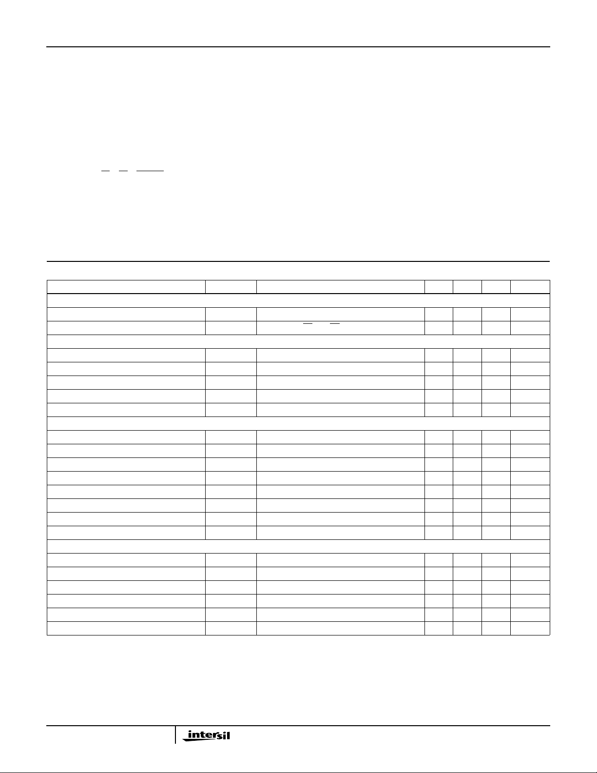
Electrical Specifications Recommended Operating Conditions, Unless Otherwise Noted. Refer to Figures 1, 2 and 3
VCC SUPPLY CURRENT
Operating Supply Current I
Shutdown Supply Current I
POWER-ON RESET, SOFT-START, AND 12V MONITOR
Rising 5VSB POR Threshold - - 4.5 V
5VSB POR Hysteresis - 0.2 - V
Rising 12V Threshold - - 10.8 V
Soft-Start Current -10- µA
Shutdown Soft-Start Voltage - - 0.8 V
2.5V/3.3V LINEAR REGULATOR (V
Regulation - - 2.0 %
VSEN2 Nominal Voltage Level V
VSEN2 Nominal Voltage Level V
VSEN2 Under-voltage Rising Threshold -75- %
VSEN2 Under-voltage Hysteresis -6- %
VSEN2 Output Current I
DRV2 Output Drive Current I
DRV2 Output Impedance R
3.3VDUAL LINEAR REGULATOR (V
Sleep-Mode Regulation - - 2.0 %
3V3DL Nominal Voltage Level V
3V3DL Under-voltage Rising Threshold - 2.450 - V
3V3DL Under-voltage Hysteresis - 200 - mV
3V3DLSB Output Drive Current I
DLA Output Impedance -90- Ω
. . . . . . . . . . . . . . . . . . . . . . . . . . . . . . +7.0V
5VSB
Thermal Resistance (Typical, Note 1) θJA (oC/W)
SOIC Package. . . . . . . . . . . . . . . . . . . . . . . . . . . . . 100
+0.3V
12V
Maximum Junction Temperature . . . . . . . . . . . . . . . . . . . . . . .150oC
Maximum Storage Temperature Range. . . . . . . . . . -65oC to 150oC
Maximum Lead Temperature (Soldering 10s) . . . . . . . . . . . . .300oC
(SOIC - Lead Tips Only)
. . . . . . . . . . . . . . . . . . . . . . . . . . . +5V ±5%
5VSB
S3,VS5,VEN3VDL,VEN5VDL
. . . . . . . . . . . . . . . . . . . . +12V ±10%
12V
. . . . . . . . . 0 to +5.5V
PARAMETER SYMBOL TEST CONDITIONS MIN TYP MAX UNITS
-20- mA
- 3.3 - V
OUT2
OUT1
5VSB
5VSB(OFF)VSS
)
VSEN2RSEL
VSEN2RSEL
VSEN2
DRV2
)
3V3DL
3V3DLSB
= 0.8V, S3 = 0, S5 = 0 - 10 - mA
= 1kΩ - 2.5 - V
= 10kΩ - 3.3 - V
5VSB = 5V 250 300 - mA
5VSB = 5V, R
= 10kΩ - 200 - Ω
SEL
= 1kΩ 20 30 - mA
SEL
5VSB = 5V 5.0 8.5 - mA
4
HIP6501A
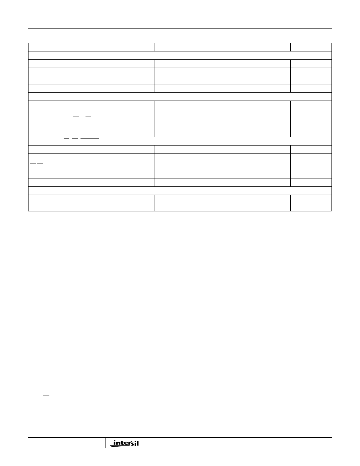
Electrical Specifications Recommended Operating Conditions, Unless Otherwise Noted. Refer to Figures 1, 2 and 3 (Continued)
PARAMETER SYMBOL TEST CONDITIONS MIN TYP MAX UNITS
5VDUAL SWITCH CONTROLLER (V
5VDL Under-Voltage Rising Threshold - 3.750 - V
5VDL Under-Voltage Hysteresis - 260 - mV
5VDLSB Output Drive Current I
5VDLSB Pull-up Impedance to 5VSB - 350 - Ω
TIMING INTERVALS
Active State Assessment Past 12V
Threshold
Maximum Allowable S3 to S5 Skew - 200 - µs
5VSB POR Extension Past Threshold
Voltage
CONTROL I/O (S3, S5, EN3VDL, EN5VDL, FAULT)
High Level Threshold - - 2.2 V
Low Level Threshold 0.8 - - V
S3,S5 Internal Pull-up Impedance to 5VSB - 70 - kΩ
FAULT Output Impedance FAULT = high - 100 - Ω
FAULT Under-Voltage Reporting Delay -10- µs
TEMPERATURE MONITOR
Fault-Level Threshold Note 3 125 - Shutdown-Level Threshold Note 3 - 150 -
NOTES:
2. Guaranteed by Correlation.
3. Guaranteed by Design.
OUT3
)
5VDLSB
5VDLSB = 4V -20 - -40 mA
Note 2 40 50 60 ms
- 3.3 - ms
o
C
o
C
Functional Pin Description
5VSB (Pin 1)
Provide a 5V bias supply for the IC to this pin by connecting
it to the ATX 5VSB output. This pin also provides the base
bias current for all the external NPN transistors controlled by
the IC. The voltage at this pin is monitored for power-on
reset (POR) purposes.
GND (Pin 8)
Signal ground forthe IC.All voltage levelsare measured with
respect to this pin.
S3 and S5 (Pins 6 and 7)
These pins switch the IC’s operating state from active (S0,
S1) to S3 and S4/S5 sleep states. Connect
and
S5 to SLP_S5. These are digital inputs featuring internal
70kΩ (typical) resistor pull-ups to 5VSB. Internal circuitry deglitches the S3 pin for disturbances. Additional circuitry
blocks any illegal state transitions (such as S3 to S4/S5 or
vice versa). When entering an S4/S5 sleep state, the
signal is allowed to go low as far as 200µs (typically) ahead
of the
S5 signal.
S3 to SLP_S3
S3
EN3VDL and EN5VDL (Pins 2 and 5)
These pins control the logic governing the output behavior in
response to S3 and S4/S5 requests. These are digital inputs
whose status can only be changed during active states
operation or during chip shutdown (SS pin grounded by
external open-drain device). The input information is latchedin when entering a sleep state, as well as following 5VSB
POR release or exit from shutdown.
FAULT/MSEL (Pin 9)
This is a multiplexed function pin allowing the setting of the
memory output voltageto either 2.5V or 3.3V (for RDRAM or
SDRAM memory systems). The memory voltage setting is
latched-in 3ms (typically) after 5VSB POR release. In case
of an under-voltage on any of the outputs or an overtemperature event, this pin is used to report the fault
condition by being pulled to 5VSB.
SS (Pin 13)
Connect a small ceramic capacitor (allowable range: 5nF-
0.22µF; 0.1µF recommended) from this pin to GND. The
internal Soft-Start (SS) current source along with the
external capacitor creates a voltage ramp used to control the
ramp-up of the output voltages. Pulling this pin low with an
open-drain device shuts down all the outputs as well as
5
 Loading...