

Page 1
TM
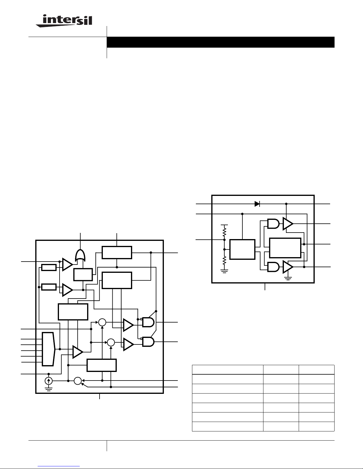
FIGURE 2. HIP6601A BLOCK DIAGRAM
PVCC 7 2 BOOT
VCC 6
CONTROL
LOGIC
SHOOT
THROUGH
PROTECTION
+5V
PWM 3
10k
UGATE
PHASE
LGATE
1
8
5
4
GND
10k
HIP6302EVAL1 - Multiphase Power Conversion
for AMD Athlon Processors up to 35A
Application Note February 2002
Introduction
Each generation of computer microprocessor brings
performance advances in computing power. Performance
improvements are made possible by advances in fabrication
technology that enable greater device density. Newer
processors are operating at lower voltages and higher clock
speeds both of which contribute to greater demands on the
microprocessor core voltage supply in terms of higher peak
currents and higher current-slew rates.
Intersil’s family of multi-phase DC-DC converter solutions
provide the ideal solution to supply the core-voltage needs of
present and future high-performance microprocessors.
Intersil HIP6302 and HIP6601
The HIP6302 controller IC works with two HIP6601A or
HIP6603A single-channel driver ICs or a single HIP6602A
dual-channel driver IC [3] to form a highly integrated solution
for high-current, high slew-rate applications. The HIP6302
regulates output voltage, balances load currents and
provides protective functions for two synchronous-rectified
buck-converter channels.
AN9888.1
Author: Matt Harris
provides feedback for droop compensation and over-current
protection. A five-bit DAC provides a digital interface to
program the 1% accurate reference and a window
comparator toggles PGOOD if the output voltage is out of
range and acts to protect the load in case of over voltage.
For more detailed descriptions of the HIP6302 functionality,
refer to the HIP6302 Data Sheet [1].
The HIP6601A is a driver IC capable of delivering up to 2A of
gate-charging current for rapidly switching both MOSFETs in
a synchronous-rectified bridge. The HIP6601A accepts a
single logic input to control both upper and lower MOSFETs.
Adaptive shoot-through protection is provided on both
switching edges to provide optimal dead time, and bootstrap
circuitry permits greater enhancement of the upper
MOSFET. For a more detailed description of the HIP6601A,
refer to the HIP6601A Data Sheet [2].
PGOOD VCC
15
VSEN
10
x 0.9
x 1.15
COMP
6
1VID4
2VID3
3VID2
DAC
4VID1
5VID0
7FB
The integrated high-bandwidth error amplifier provides
voltage regulation, while current-sense circuitry maintains
UV
+
OV
LATCH
S
OVP
+
-
SOFT START
AND FAULT
LOGIC
+
-
∑
FIGURE 1. HIP6302 BLOCK DIAGRAM
+
-
E/A
CURRENT
DETECTION
+
+
9
phase-current balance between the two power channels and
16
POWER-ON
RESET (POR)
THREE STATE
CLOCK AND
SAWTOOTH
GENERATOR
∑
+
∑
-
GND
PWM
+
-
PWM
+
-
8
FS/DIS
13
PWM1
12
PWM2
1411ISEN1
ISEN2
The HIP6302EVAL1 Board and Reference
Design
With the VID jumpers set to 1.7V (00110), the evaluation
board meets the output voltage and current specifications
indicated in Table 1.
TABLE 1. HIP6302EVAL1 OUTPUT PARAMETERS
MIN MAX
Static Regulation 1.65V 1.75V
Transient Regulation 1.60V 1.85V
Over-Voltage Protection 1.90V 2.00V
Continuous Load Current - 35A
Over-Current Trip Level 41A 57A
Load-Current Transient - 35A/µs
1
CAUTION: These devices are sensitive to electrostatic discharge; follow proper IC Handling Procedures.
1-888-INTERSIL or 321-724-7143
|
Intersil (and design) is a trademark of Intersil Americas Inc.
Copyright © Intersil Americas Inc. 2002. All Rights Reserved
Page 2
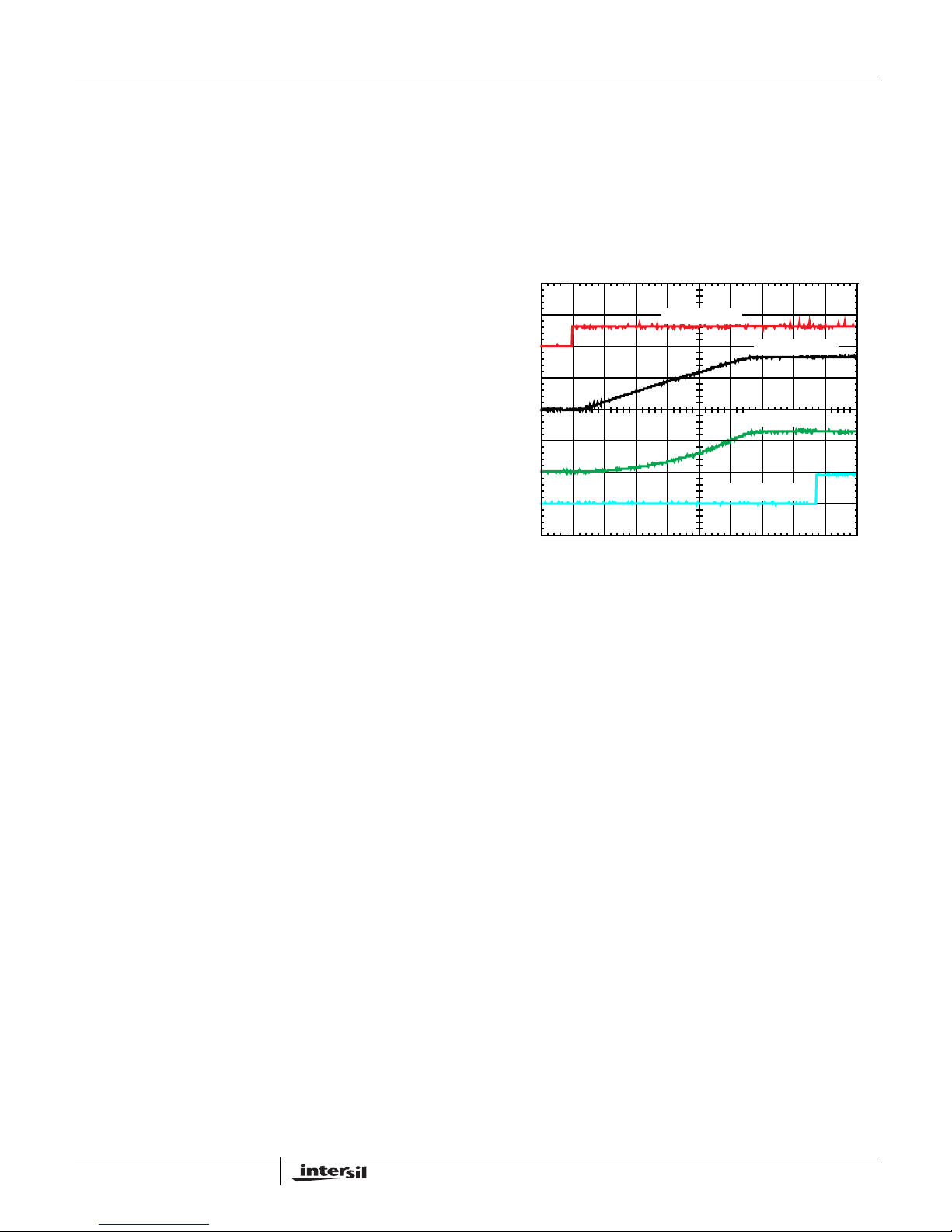
PGOOD, 5V/DIV
1ms/DIV
0A
0V
0V
0V
ICC5, 10A/DIV
VCORE, 1V/DIV
FS/EN, 5V/DIV
FIGURE 3. HIP6302EVAL1 START-UP WAVEFORMS
Application Note AN9888
The HIP6302EVAL1 evaluation board incorporates a
reference design intended to meet the core-voltage
requirements for AMD Athlon
microprocessors up to 35A.
Additional circuitry is provided to facilitate circuit evaluation
including input and output power connectors, VID jumpers,
numerous probe points, an LED power-good indicator, and a
load-transient generator.
Powering the HIP6302EVAL1
For convenience, the HIP6302EVAL1 provides two methods
of making input power connections. The 20-pin header, J1,
interfaces with a standard ATX power supply and may be the
most convenient method of powering the board.
J2, J3, and J4 are standard banana-jack connectors that can
be used to supply power using bench-top power supplies.
These inputs provide greater versatility in testing and design
validation by allowing the 12V and 5V power-input voltage
levels to be varied independently. In this way power-on level
and power-sequencing issues can be easily examined.
To start the evaluation board, insert the 20-pin connector
from an ATX supply into J1. If using bench-top supplies,
connect a 12V supply to J2 and a 5V supply to J3. Connect
the grounds from both supplies to J4.
Start Up
The waveforms in Figure 3 demonstrate the normal start-up
sequence with the HIP6302EVAL1 connected to a 55m
load. After FS/EN is released, VCORE exhibits a linear ramp
until reaching its 1.7V set point. The gradual increase of
VCORE over approximately 5ms limits the current required
from the input supply, ICC5, to a level that does not strain the
supply. The HIP6302 asserts PGOOD once VCORE is within
regulation limits.
Ω
Important
There are two things to consider when using bench-top
supplies. If the 5V supply is applied prior to the 12V supply,
the HIP6302 will begin operating before the HIP6601As. This
allows the HIP6302 to complete its soft-start cycle before the
drivers are capable of switching power to the output. When
the 12V power input is then applied, there is a large transient
as the controller tries to instantly bring the output to its fullvoltage level. This can result in an overcurrent protection
cycle and an abnormal start-up waveform. It can be avoided
by applying 5V supply after or at the same time as the 12V
supply or by using an ATX power supply.
The second problem can occur when operating the transient
load generator. Not all bench-top and ATX power supplies
are capable of responding to load transients, and they may
allow a momentary voltage dip on VCC5. This can activate
the power-on-reset function in the HIP6302 and cause the
output power to cycle. It can be remedied by connecting a
5600
µ F or larger capacitor between VCC5 and ground. The
capacitor, if necessary, simulates the distributed capacitance
that exists on the computer motherboard.
Transient Response
The HIP6302EVAL1 is equipped with a load-transient
generator that applies a 0–36A transient load current with
rise and fall rates of approximately 35A/
the transient is between 100
µ
s and 200 µ
rate is kept low in order to limit power dissipation in the load
MOSFETs and resistors. Removal of the HI/LO jumper (JP2)
causes the current to decrease from about 36A to about
31A. The load-transient generator operates when the
HIP6302EVAL1 is properly connected to a 12V power
source and SW1 is in the ON position. Operation ceases
when SW1 is moved into the OFF position or 12V is
removed from the board.
The HIP6302EVAL1 achieves the specified transient
performance while maintaining a favorable balance between
low cost, high efficiency and small profile. When the duty
cycle changes rapidly in response to a transient load current,
the inductor current immediately begins to change in order to
meet the demand. During the time the inductor current is
increasing, the output-filter capacitors are supplying the
load. It follows that the amount of required capacitance
decreases as the capability of the inductors to rapidly
assume the load current increases.
µ
s. The duration of
s, and the repetition
2
Athlon™ is a trademark of Advanced Micro Devices, Inc.
Page 3
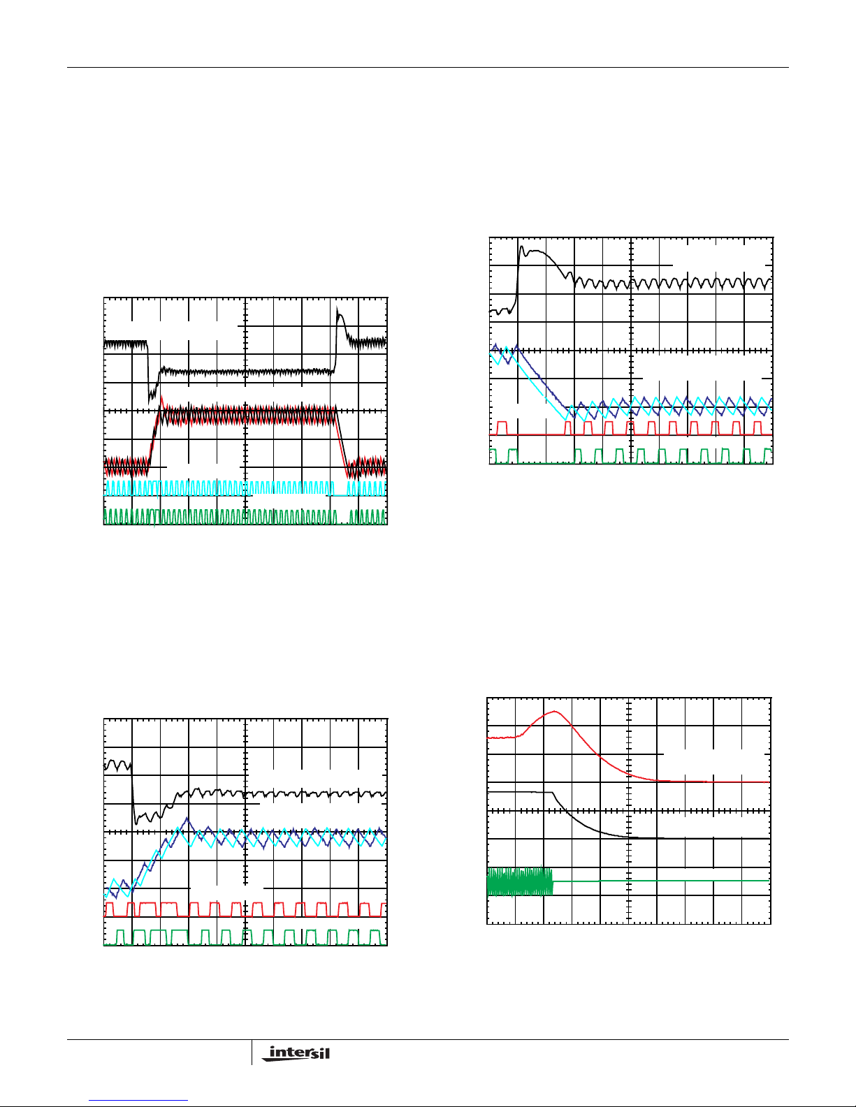
3
5µs/DIV
0V
0A
1.7V
0V
PWM2, 10V/DIV
CORE VOLTAGE,
FIGURE 6. TRANSIENT-RESPONSE TRAILING EDGE
PWM1, 10V/DIV
INDUCTOR CURRENTS,
10A/DIV
50mV/DIV
FIGURE 7. OVERCURRENT BEHAVIOR
50µs/DIV
0A
0V
0V
CORE VOLTAGE,
OUTPUT CURRENT,
PWM1, 5V/DIV
20A/DIV
500mV/DIV
Application Note AN9888
Figure 4 shows the core voltage, inductor current, and PWM
signals changing in response to the transient load current.
The upper waveform shows the core voltage deviating from
its no-load setting of 1.72V to a minimum of about 1.62V
upon the application of current. The voltage then settles to its
1.67V full-load setting. On load removal, the core voltage
peaks at a level of 1.78V before settling again to its 1.72V
no-load setting. Although the specified operating range
allows deviations as low as 1.60V and as high as 1.85V, a
minimum of 20mV is reserved to allow for the reference
tolerance and the tolerances of other components that
contribute to the overall system accuracy.
CORE VOLTAGE, 50mV/DIV
1.7V
INDUCTOR CURRENTS, 10A/DIV
0A
0V
0V
FIGURE 4. HIP6302EVAL1 TRANSIENT RESPONSE
PWM1, 10V/DIV
PWM2, 10V/DIV
20µs/DIV
Figure 5 is a close-up showing the core-voltage, inductorcurrent and PWM signals responding at the leading edge of
the transient load
current. The PWM signals increase to their
maximum duty cycle of 75% on the first pulse following the
start of the transient. The inductor currents begin to increase
immediately and are carrying all of the load within 10
µ s. The
very fast transient response is due to the precision 18MHz
error amplifier and optimal compensation of the control loop.
The close up in Figure 6 shows the core-voltage, inductorcurrent and PWM signals changing in response to the
trailing edge of the transient load current. Again, the duty
cycles immediately decrease to zero, and the inductors
begin shedding load current at the maximum rate. Note that
the inductor currents briefly go negative as the transient
settles. The capacitors are slightly over charged at the end of
the transient, and the discharge path is in the reverse
direction through the inductors.
Overcurrent Protection
µ
When the current out of either ISEN pin exceeds 82
HIP6302 detects an overcurrent condition and responds by
placing the PWM outputs into a high-impedance state. This
signals the HIP6601 to turn off both upper and lower
MOSFETs in order to remedy the overcurrent condition.This
behavior is seen in Figure 7 where PWM1 goes immediately to
2.5VDC when the output current reaches approximately 50A.
The output voltage then quickly falls to zero.
A, the
1.7V
CORE VOLTAGE, 50mV/DIV
INDUCTOR CURRENTS,
10A/DIV
0A
0V
0V
FIGURE 5. TRANSIENT-RESPONSE LEADING EDGE
PWM1, 10V/DIV
5µs/DIV
PWM2, 10V/DIV
Page 4
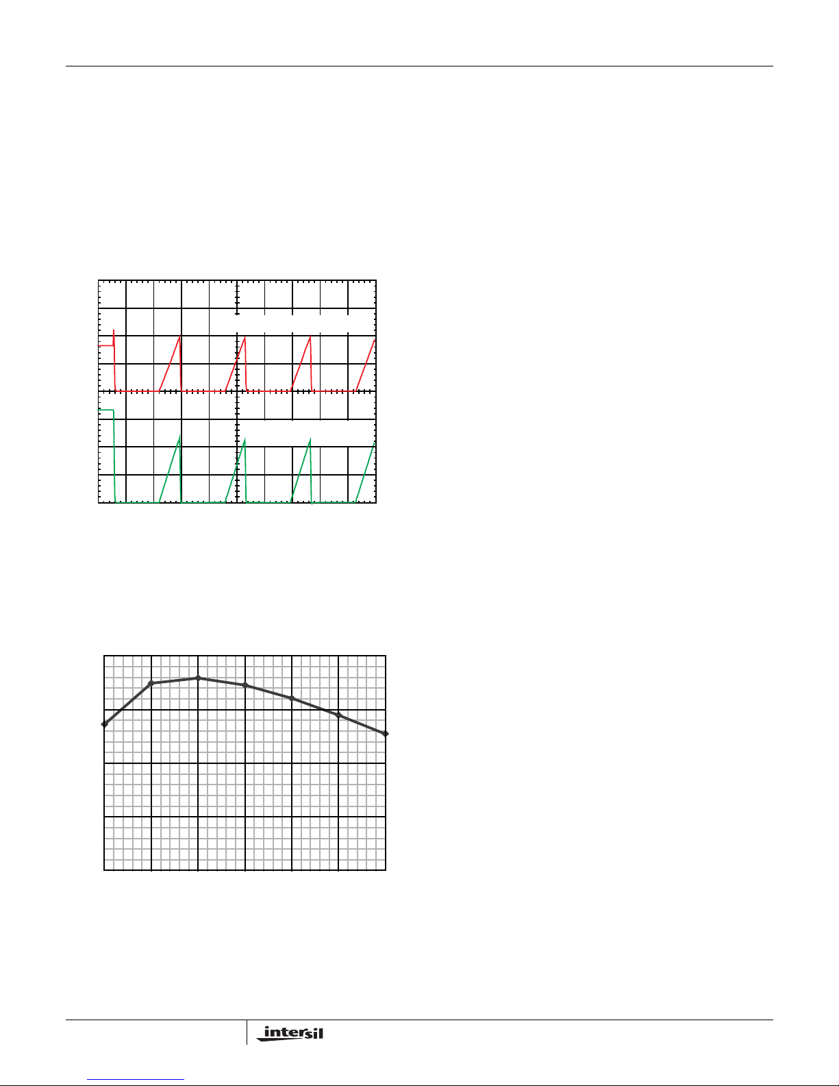
4
Application Note AN9888
After the initial over-current trip, the HIP6302 waits for a
period of time equal to 2048/f
SW
(f
is the switching
SW
frequency) before initiating a soft-start cycle. If the over-load
condition remains, another over-current trip will occur before
the end of the soft-start sequence. This repetitive overcurrent cycling is illustrated in Figure 8, and will continue
indefinitely unless the fault is cleared or power to the
converter is removed. Because of the wait period, the worst
case power delivered during overcurrent cycling is equal to
45% of the power delivered during normal operation at full
load. Therefore, indefinite over-current cycling does not
create a thermal problem for the circuit.
OUTPUT CURRENT, 20A/DIV
0A
CORE VOLTAGE,
500mV/DIV
0V
FIGURE 8. OVERCURRENT BEHAVIOR
5ms/DIV
Efficiency
Figure 9 shows the efficiency versus current plot for the
HIP6302EVAL1 for 5A through 35A. The measurements
were made at room temperature with natural convection
cooling only..
90
Summary
The HIP6302EVAL1 is intended to provide a convenient
platform to evaluate the performance of the HIP6302 HIP6601A chip set in the specific implementation indicated
in Table 1. The design demonstrates a favorable trade off
between low cost, high efficiency, and small footprint. The
following pages include schematic, bill of materials, and
layout drawings to facilitate implementation of this solution.
The evaluation board is simple and convenient to operate,
and test points are available to evaluate the most commonly
tested parameters. Example waveforms are given for
reference.
The HIP6302 and HIP6601A provide a versatile 2-phase
power solution for low-voltage applications from 25A to
approximately 40A, and together they result in the most
effective solution available.
References
For Intersil documents available on the internet, see web site
http://www.intersil.com/
Intersil Technical Support 1 (888) INTERSIL
[1] HIP6302 Data Sheet, Intersil Corporation, Power
Management Products Division, 2000.
(http://www.intersil.com/).
[2]
HIP6601A, HIP6603A Data Sheet,
Power Management Products Division, 2000.
[3]
HIP6602A Data Sheet,
Intersil Corporation, Power
Management Products Division, 2000.
Intersil Corporation,
85
80
EFFICIENCY (%)
75
70
5101520253035
CURRENT (AMPERES)
FIGURE 9. EFFICIENCY vs CURRENT
Page 5

Schematic
Application Note AN9888
5VIN
12VIN
C7
0.1µF
JP1
R3
107kΩ
16
VCC
9
GND
1
VID4
2
VID3
3
VID2
4
VID1
5
VID0
HIP6302
15
PGOOD
FS/DIS
COMP
6710
TP7
FB
R4
14.0kΩR51.00kΩ
C11
2.2nF
R6
45.3kΩ
PWM1
ISEN1
PWM2
ISEN2
VSEN
1µF
13 3
TP3
14
C12
1µF
12
TP4
11
C6
6
VCC
HIP6601
R1
2.15kΩ
672
VCC
3
PWM
HIP6601
R2
2.15kΩ
72
BOOT
UGATE
PVCC
PHASEPWM
LGATE
GND
4U1
BOOT
UGATE
PVCC
PHASE
LGATE
GND
4U3
L1
1µF
C4
C3
0.1µF
1
8
5
TP2
C8
0.1µF
1
8
5
Q1
HUF76139
Q2
HUF76139
TP1
Q3
HUF76139
Q4
HUF76139
TP6
TP5
C13-C17
1µF
L2
450nH
C9
1µF
L3
450nH
22µF
C5
100µFC11000µF
C10
100µFC21000µF
C18-C21
560µF
R8
10kΩR71kΩR91kΩ
RED GREEN
CR1
Q5
2N7002
POWER GOOD INDICATOR
D1
BAV99
R15
0.200Ω
HUF76129
Q6
HUF76129
Q7
R14, R16
0.100Ω
R10
1.50kΩ
R11
619Ω
C48
1µF
TP11
R17
46.4kΩ
TRANSIENT GENERATOR
12 6
4
HS
7
VSS
Q8
2N7002
D2
BAV99
HB
VDD
U4
HIP2100
R18
400Ω
HO
LO
HI
JP2
LI
3
8
SW1
ON
C49
10µF
R12
1.50kΩ
R13
619Ω
OFF
5
Page 6

Application Note AN9888
Bill of Materials
QTY REFERENCE DESCRIPTION PACKAGE VENDOR PART NO.
1 CR1 RED/GREEN LED SMT Lumex SSL-LXA3025IGC
2 C1, C2 1000
3 C3, C7, C8 0.1
5 C4, C6, C9, C12, C48 1.0
2 C5, C10 100
1 C11 2.2nF, 50V, X7R, Ceramic Capacitor 0603 Various
5 C13-C17, C49 10
4 C19, C20, C22, C23 560
2 C18, C21 Spare Radial
24 C24-C47 Spare 1206
2 D1, D2 Dual Diode SOT23 Various BAV99
1 JP1 5-Position Jumper Header 100mil Centers Berg 68000-236
5 Jumpers Berg 71363-102
1 JP2 1-Position Header 100mil Centers Berg 68000-236
1 Jumper Berg 71363-102
1J1 ATX Power Header Berg 39-29-9203
2 J2, J3 Female Banana Connector, Red Johnson
1J4 Female Banana Connector, Black Johnson
2 J5, J6 Terminal Connector Burndy KPA8CTP
1L1 1uH, T30-26, 6T AWG18 400x300mil Falco TTIG0803-127
2 L2, L3 450nH, T60-8/90, 5T AWG14 700x500mil Falco TTIB1506-478
4 Q1, Q2, Q3, Q4 Power MOSFETs TO-263AB Intersil HUF76139S3S
2 Q5, Q8 General Purpose MOSFET SOT23 Various 2N7002
2 Q6, Q7 Power MOSFET TO-252AA Intersil HUF76129D3S
2 R1, R2 Resistor, 2.15k
1R3 Resistor, 107k
1R4 Resistor, 14.0k
1R5 Resistor, 1.00k
1R6 Resistor, 45.3k
2 R7, R9 Resistor, 1.0k
1R8 Resistor, 10k
2 R10, R12 Resistor, 1.50k
2 R11, R13 Resistor, 619
2 R14, R16 Resistor, 0.100
1 R15 Resistor, 0.200
1 R17 Resistor, 46.4k
1 R18 Resistor, 400
1 SW1 Switch, SPDT SMT C&K Components GT11MSCKE
6 TP1, TP3, TP4, TP5, TP7, TP8 Small Test Point Jolo SPCJ-123-01
3 TP2, TP6, TP10 Large Test Point Keystone 1514-2
2 TP9, TP11 Probe Socket Tektronics 1314353-00
2 U1, U3 Synchronous Buck Driver IC 8-Lead SOIC Intersil HIP6601ACB
1U2 Multiphase Buck Controller IC 16-Lead SOIC Intersil HIP6302CB
1U4 MOSFET Driver IC 8-Lead SOIC Intersil HIP2100IB
µ F, 10V, Aluminum Capacitor Radial Panasonic EEUFC1A102L
µ
F, 25V, Y5V, Ceramic Capacitor 0603 Various
µ F, 25V, Y5V, Ceramic Capacitor 0805 Various
µ
F, 16V, OS-CON Capacitor Radial Sanyo 16SPS100M
µ
F, 10V, X7R, Ceramic Capacitor 1206 Various
µ F, 4V, OS-CON Capacitor Radial Sanyo 4SP560M
111-0702-001
Components
111-0703-001
Components
Ω
, 1%, 1/10W 0603 Various
Ω , 1%, 1/10W 0603 Various
Ω
, 1%, 1/10W 0603 Various
Ω , 1%,1/10W 0603 Various
Ω
, 1%, 1/10W 0603 Various
Ω , 5%, 1/8W 0805 Various
Ω , 5%, 1/10W 0603 Various
Ω , 1%, 1/8W 0805 Various
Ω , 1%, 1/8W 0805 Various
Ω , 1%, 1W 2512 Vishay WSL2512R100FB43
Ω
, 1%, 1W 2512 Vishay WSL2512R200FB43
Ω , 1%,1/8W 0805 Various
Ω , 1%, 1/8W 0805 Various
6
Page 7

Layout Drawing - Components
Application Note AN9888
7
Page 8

Layout Drawing - Top Copper
Application Note AN9888
8
Page 9

Layout Drawing - Ground Plane
Application Note AN9888
9
Page 10

Layout Drawing - Power Plane
Application Note AN9888
10
Page 11

Layout Drawing - Bottom Copper
Application Note AN9888
11
All Intersil U.S. products are manufactured, assembled and tested utilizing ISO9000 quality systems.
Intersil Corporation’s quality certifications can be viewed at www.intersil.com/design/quality
Intersil products are sold by description only. Intersil Corporation reserves the right to make changes in circuit design, software and/or specifications at any time without
notice. Accordingly, the reader is cautioned to verify that data sheets are current before placing orders. Information furnished by Intersil is believed to be accurate and
reliable. However, no responsibility is assumed by Intersil or its subsidiaries for its use; nor for any infringements of patents or other rights of third parties which may result
from its use. No license is granted by implication or otherwise under any patent or patent rights of Intersil or its subsidiaries.
For information regarding Intersil Corporation and its products, see www.intersil.com
Page 12

Mouser Electronics
Authorized Distributor
Click to View Pricing, Inventory, Delivery & Lifecycle Information:
Intersil:
HIP6302EVAL1
 Loading...