

Intersil Corporation HIP6201, HIP6200 Datasheet

HIP6200, HIP6201
Data Sheet February 1998
Transient Voltage Regulator
DeCAPitator™
The Intersil DeCAPitator helps to stabilize a power system
voltage during severe transients. It accomplishes this by
supplying current when the voltage is more than 1% low or
sinking current when the voltage is higher than 1.5% from
the average load voltage. The fast transient response of the
DeCAPitator can make up for the slow response time of
many switching DC-DC converters.
Although the HIP6200 serves as a simple replacement for
large output capacitors for any dynamic load, it is especially
useful in stabilizing the CPU core voltage in portable
computer applications, where size and efficiency are major
concerns. The DeCAPitator enables power supply designs
for more powerful microprocessors without increasing
converter size or decreasing converter efficiency.
The DeCAPitator acts independently of the PWM control
circuitry. This simplifies converter layout because the
DeCAPitator and the load may be located separately from
the DC-DC converter. The DeCAPitator should be located
near the load for optimum performance.
File Number
4423.2
Features
• Saves Power System Size and Cost
- Replaces Expensive Bulk Capacitors
- Small 8 Lead SOIC Package
• Linear Regulator Response
- Greater than 5MHz Bandwidth
• Very Low Static Power Dissipation
- Shutdown Current. . . . . . . . . . . . . . . . . . . . . . . . . < 5µA
- Power Dissipated Only During Load Transients
• Over Temperature Shutdown/Signal
• Simplifies Power Supply Layout
- Allows for Remotely Located CPU DC-DC Converter
Applications
• Notebook Computers
• Pentium®, Pentium Pro, and Pentium II Power Supplies
Ordering Information
TEMP.
PART NUMBER
HIP6200CB 0 to 70 8 Ld SOIC M8.15
HIP6201CB 0 to 70 8 Ld SOIC M8.15
RANGE (oC) PACKAGE
PKG.
NO.
Pinouts
PV
CC
PGND
GND
V
CC
HIP6200 (SOIC)
TOP VIEW
1
2
3
4
2-441
8
7
6
5
EN/OT
OUT
SNS
CAP
HIP6201 (SOIC)
TOP VIEW
PV
1
CC
PGND
2
GND
3
4
V
CC
Pentium® is a registered trademark of Intel Corporation.
DeCAPitator™ is a trademark of Intersil Corporation.
CAUTION: These devices are sensitive to electrostatic discharge; follow proper IC Handling Procedures.
http://www.intersil.com or 407-727-9207
| Copyright © Intersil Corporation 1999
EN
8
OUT
7
SNS
6
5
CAP
HIP6200, HIP6201
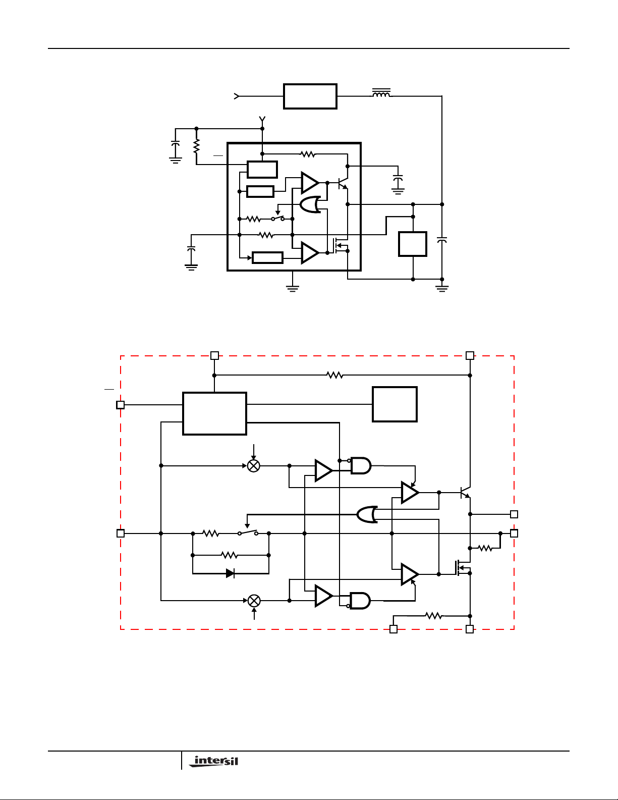
Typical Application - Portable CPU Dynamic Regulator
Block Diagram
EN/OT
(HIP6200)
EN
(HIP6201)
BATTERY
POWER
EN/OT
CAP
V
CC
POWER-ON
RESET (POR)
PWM
CONTROLLER
+5V
V
CC
4
8
POR
X 0.99
R
5
X 1.015
20R
GND
HIP6200
+
-
+
-
3
PGND
R
VCC
PV
1
CC
OUT
7
SNS
6
2
LOAD
THERMAL
MONITOR
(TMON)
CPU
P
VCC
CAP
99%
R
T1
R
T2
101.5%
UPPER
COMPARATOR
+
-
+
-
LOWER
COMPARATOR
ENABLE
+
LOWER
AMPLIFIER
+
ENABLE
UPPER
AMPLIFIER
-
-
R
GND
OUT
SNS
R
OUT
PGNDGND
2-442

HIP6200, HIP6201
Functional Pin Description
P
(Pin 1)
VCC
P
is the power source for the npn transistor output
VCC
device. P
resistor.Bulkcapacitance should be placed between this pin
and PGND to minimize voltage deviations.
PGND (Pin 2)
PGND is power ground for the N-Channel MOSFET output
device. Tie this pin to the ground plane of the circuit board.
GND (Pin 3)
GND is signal ground for the IC. Tie this pin to the ground
plane of the circuit board.
VCC (Pin 4)
VCC provides bias power to the chip. It should be tied to
system 5V. Provide local decoupling to this pin.
CAP (Pin 5)
Connect a capacitor to GND to set the internal amplifiers’
on-time response to a rapid voltage change at the SNS pin.
is connected internally to VCC through a
VCC
SNS (Pin 6)
SNS is the remote sense of the output voltage to be
regulated. If the output voltage increases rapidly by greater
than 1.5%, the lower amplifier responds by turning on the NChannel MOSFET to sink current through the OUT pin to
PGND. If the output voltage decreases rapidly by greater
than 1%, the upper amplifier responds by turning on the npn
transistor to source current from P
VCC
to OUT.
OUT (Pin 7)
This pin is the output pin of the IC. Tie this pin directly to the
voltage to be regulated.
EN/OT or EN (Pin 8)
This pin is the only differentiation between the HIP6200 and
the HIP6201.
On the HIP6200, this pin is multiplexed.It is chip enable and
also an overtemperature indicator. When this pin is low, the
chip is disabled.Ifanovertemperature occurs, this pin will be
pulled low internally. Tie EN/
drive with an open collector signal.
On the HIP6201, this pin is chip enable only. Pulling it low
disables the IC. EN should be driven with a logic signal.
OT to a pull-up resistor and
2-443
 Loading...