

HIP6021A
Data Sheet November 1999
Advanced PWM and Triple Linear Power
Controller
The HIP6021A provides the power control and protection for
four output voltages in high-performance, graphics intensive
microprocessor and computer applications. The IC
integrates a voltage-mode PWM controller and three linear
controllers, as well as the monitoring and protection
functions into a 28 lead SOIC package.
The synchronous-rectified buck converter includes an Intelcompatible, TTL 5-input digital-to-analog converter (DAC)
that adjusts the core PWM output voltage from 1.3V
2.05V
in 0.05V steps and from 2.1VDCto 3.5VDCin 0.1V
DC
DC
to
increments. The precision reference and voltage-mode
control provide ±1% static regulation. A TTL-compatible
signal applied to the SELECT pin dictates which method of
control is used for the AGP bus power: a low state results in
linear control of the AGP bus to 1.5V, while a high state
transitions theoutputthrough a linearly controlled softstart to
3.3V, followed by full enhancement of the external MOSFET
to pass the input voltage. The other two linear regulators
provide fixed output voltages of 1.5V GTL bus power and
1.8V power for the North/South Bridge core and/or cache
memory. These levels are user-adjustable by means of an
external resistor divider and pulling the FIX pin low. All linear
controllers can employ either N-Channel MOSFETs or
bipolar NPNs for the pass transistor.
The HIP6021A monitors all the output voltages. A single
Power Good signal is issued when the core is within ±10% of
the DAC setting and all other outputs are above their undervoltage levels. Additional built-in over-voltage protection for
the core output uses the lower MOSFET to prevent output
voltages above 115% of the DAC setting. The PWM
controller’s over-current function monitors the output current
by using the voltage drop across the upper MOSFET’s
r
DS(ON)
.
Ordering Information
TEMP.
PART NUMBER
HIP6021ACB 0 to 70 28 Ld SOIC M28.3
HIP6021EVAL1 Evaluation Board
RANGE (oC) PACKAGE
PKG.
NO.
File Number 4793
Features
• Provides 4 Regulated Voltages
- Microprocessor Core, AGP Bus, Memory, and GTL Bus
Power
• Drives N-Channel MOSFETs
• Linear Regulator Drives Compatible with both MOSFET
and Bipolar Series Pass Transistors
• Fixed or Externally Resistor-Adjustable Linear Outputs
• Simple Single-Loop Control Design
- Voltage-Mode PWM Control
• Fast PWM Converter Transient Response
- High-Bandwidth Error Amplifier
- Full 0% to 100% Duty Ratio
• Excellent Output Voltage Regulation
- Core PWM Output: ±1% Over Temperature
- Other Outputs: ±3% Over Temperature
• TTL-Compatible 5-Bit DAC Core Output Voltage Selection
- Shutdown Feature Removed When All Inputs High
- Wide Range 1.3VDC to 3.5V
DC
• Power-Good Output Voltage Monitor
• Over-Voltage and Over-Current Fault Monitors
- Switching Regulator Does Not Require Extra Current
Sensing Element, Uses Upper MOSFET’s r
DS(ON)
• Small Converter Size
- Constant Frequency Operation
- 200kHz Free-Running Oscillator; Programmable From
50kHz to Over 1MHz
- Small External Component Count
Applications
•
Motherboard Power Regulation for Computers
Pinout
DRIVE2
PGOOD
VSEN2
SELECT
FAULT/RT
VSEN4
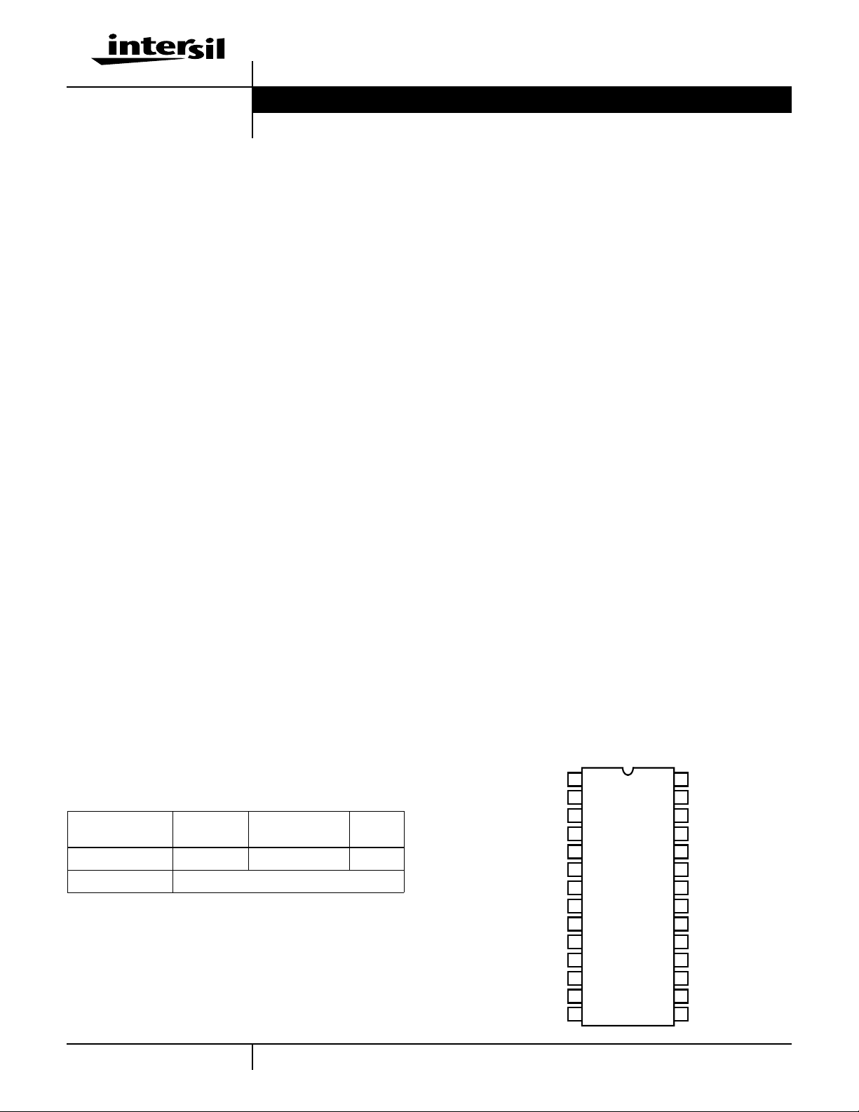
HIP6021A (SOIC)
1
2
FIX
3
VID4
4
VID3
5
VID2
6
VID1
7
VID0
8
9
SD
10
11
SS
12
13
14
TOP VIEW
28
27
26
25
24
23
22
21
20
19
18
17
16
15
VCC
UGATE
PHASE
LGATE
PGND
OCSET
VSEN1
FB
COMP
VSEN3
DRIVE3
GND
VAUX
DRIVE4
1
CAUTION: These devices are sensitive to electrostatic discharge; follow proper IC Handling Procedures.
1-888-INTERSIL or 407-727-9207
| Copyright © Intersil Corporation 1999
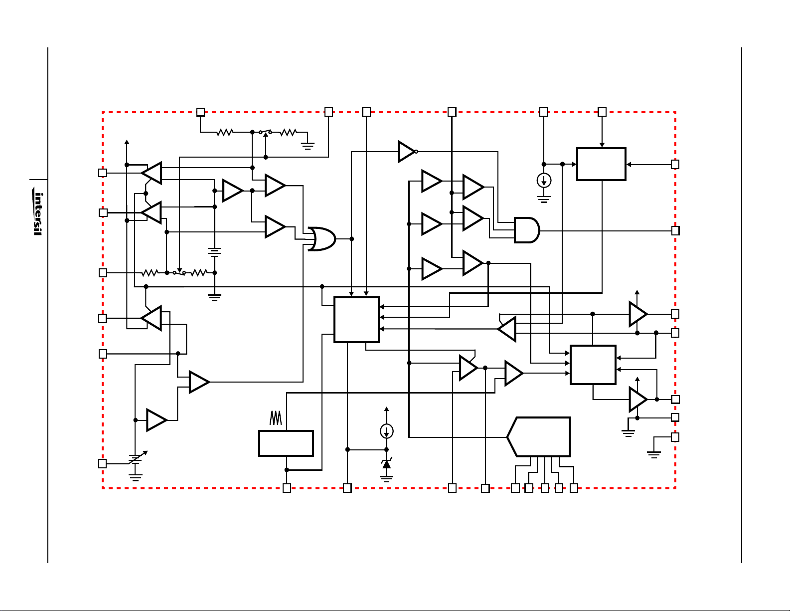
Block Diagram
OCSET
200µA
+
-
+
PWM
COMP1
TTL D/A
CONVERTER
(DAC)
PWM1
x 1.10
x 0.90
x 1.15
ERROR
AMP1
DACOUT
VSEN1
+
-
+
-
+
-
OC1
+
-
VSEN3
VAUX
2
DRIVE3
DRIVE4
VSEN4
DRIVE2
VSEN2
SELECT
-
+
+
-
+
-
+
-
x 0.75
+
1.5V
OR
-
3.3V
IN
x 0.75
+
1.26V
-
+
+
-
OSCILLATOR
FIX
LUV
LINEAR
UNDER-
VOLTAGE
INHIBIT
FAULT
SD
SOFT-
START
AND FAULT
LOGIC
28µA
OV
VCC
4.5V
VCC
POWER-ON
RESET (POR)
DRIVE1
GATE
CONTROL
SYNCH
DRIVE
VAUX
PGOOD
HIP6021A
VCC
UGATE
PHASE
VCC
LGATE
PGND
GND
FAULT / RT
SS
FB
COMP
VID0
VID1
VID2
VID4
VID3
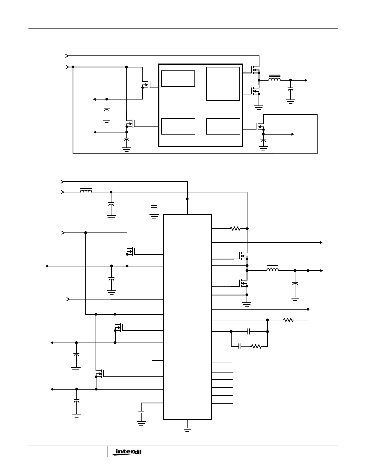
Simplified Power System Diagram
+5V
IN
+3.3V
IN
Q3
V
OUT2
HIP6021A
LINEAR
CONTROLLER
HIP6021A
PWM
CONTROLLER
Q1
Q2
V
OUT1
V
Typical Application
+12V
IN
+5V
IN
+3.3V
IN
V
OUT2
1.5V OR 3.3V
TYPEDET
V
OUT3
1.5V
IN
L
IN
OUT3
Q4
C
IN
Q4
C
Q3
OUT2
DRIVE2
VSEN2
SELECT
VAUX
DRIVE3
VSEN3
LINEAR
CONTROLLER
HIP6021A
VCC
LINEAR
CONTROLLER
OCSET
PGOOD
UGATE
PHASE
LGATE
PGND
VSEN1
FB
COMP
Q2
Q1
Q5
L
OUT1
C
OUT1
V
OUT4
POWERGOOD
1.3V TO 3.5V
V
OUT1
V
OUT4
1.8V
C
C
OUT3
OUT4
Q5
FIX
DRIVE4
VSEN4
SS
C
SS
GND
FAULT / RT
VID0
VID1
VID2
VID3
VID4
3
HIP6021A
Absolute Maximum Ratings Thermal Information
Supply Voltage, VCC . . . . . . . . . . . . . . . . . . . . . . . . . . . . . . . . +15V
PGOOD, RT/FAULT, DRIVE, PHASE,
and GATE Voltage . . . . . . . . . . . . . . . GND - 0.3V to VCC + 0.3V
Input, Output or I/O Voltage. . . . . . . . . . . . . . . . . . GND -0.3V to 7V
ESD Classification . . . . . . . . . . . . . . . . . . . . . . . . . . . . . . . . Class 1
Operating Conditions
Supply Voltage, VCC . . . . . . . . . . . . . . . . . . . . . . . . . . . +12V ±10%
Ambient Temperature Range. . . . . . . . . . . . . . . . . . . . 0oC to 70oC
Junction Temperature Range. . . . . . . . . . . . . . . . . . . 0oC to 125oC
CAUTION: Stresses above those listed in “Absolute Maximum Ratings” may cause permanent damage to the device. This is a stress only rating and operation of the
device at these or any other conditions above those indicated in the operational sections of this specification is not implied.
NOTE:
1. θJA is measured with the component mounted on an evaluation PC board in free air.
Electrical Specifications Recommended Operating Conditions, Unless Otherwise Noted. Refer to Block and Simplified Power System
Diagrams, and Typical Application Schematic
PARAMETER SYMBOL TEST CONDITIONS MIN TYP MAX UNITS
VCC SUPPLY CURRENT
Nominal Supply Current I
CC
POWER-ON RESET
Rising VCC Threshold V
Falling VCC Threshold V
Rising VAUX Threshold V
VAUX Threshold Hysteresis V
Rising V
Threshold - 1.26 - V
OCSET
OSCILLATOR
Free Running Frequency F
OSC
Total Variation 6kΩ < RT to GND < 200kΩ -15 - +15 %
Ramp Amplitude ∆V
OSC
DAC AND BANDGAP REFERENCE
DAC(VID0-VID4) Input Low Voltage - - 0.8 V
DAC(VID0-VID4) Input High Voltage 2.0 - - V
DACOUT Voltage Accuracy -1.0 - +1.0 %
Bandgap Reference Voltage V
BG
Bandgap Reference Tolerance -2.5 - +2.5 %
LINEAR REGULATORS (OUT2, OUT3, AND OUT4)
Regulation (All Linears) Except OUT2 when SELECT > 2.0V - 3 - %
VSEN2 Regulation Voltage VREG2SELECT < 0.8V - 1.5 - V
VSEN3 Regulation Voltage VREG
VSEN4 Regulation Voltage VREG
Under-Voltage Level (VSEN/VREG) VSEN
Under-Voltage Hysteresis (VSEN/VREG) VSEN Falling - 7 - %
Output Drive Current (All Linears) VAUX-V
UGATE, LGATE, DRIVE2, DRIVE3, and
DRIVE4 Open
OCSET
OCSET
OCSET
OCSET
RT = OPEN 185 200 215 kHz
RT = Open - 1.9 - V
3
4
VSEN Rising - 75 - %
UV
Thermal Resistance (Typical, Note 1) θJA (oC/W)
SOIC Package. . . . . . . . . . . . . . . . . . . . . . . . . . . . . 70
Maximum Junction Temperature (Plastic Package) . . . . . . . 150oC
Maximum Storage Temperature Range. . . . . . . . . . -65oC to 150oC
Maximum Lead Temperature (Soldering 10s) . . . . . . . . . . . . 300oC
(SOIC - Lead Tips Only)
-9- mA
= 4.5V - - 10.4 V
= 4.5V 8.2 - - V
= 4.5V - 2.5 - V
= 4.5V - 0.5 - V
- 1.265 - V
- 1.5 - V
- 1.8 - V
> 0.6V 20 40 - mA
DRIVE
P-P
4
HIP6021A
Electrical Specifications Recommended Operating Conditions, Unless Otherwise Noted. Refer to Block and Simplified Power System
Diagrams, and Typical Application Schematic (Continued)
PARAMETER SYMBOL TEST CONDITIONS MIN TYP MAX UNITS
SYNCHRONOUS PWM CONTROLLER ERROR AMPLIFIER
DC Gain -88- dB
Gain-Bandwidth Product GBWP - 15 - MHz
Slew Rate SR COMP = 10pF - 6 - V/µs
PWM CONTROLLER GATE DRIVER
UGATE Source I
UGATE Sink R
LGATE Source I
LGATE Sink R
UGATE
UGATEVGATE-PHASE
LGATE
LGATE
PROTECTION
VSEN1 Over-Voltage (VSEN1/DACOUT) VSEN1 Rising - 115 120 %
FAULT Sourcing Current I
OCSET1 Current Source I
Soft-Start Current I
OVP
OCSET
SS
POWER GOOD
VSEN1 Upper Threshold
(VSEN1/DACOUT)
VSEN1 Under-Voltage
(VSEN1/DACOUT)
VSEN1 Hysteresis (VSEN1/DACOUT) Upper/Lower Threshold - 2 - %
PGOOD Voltage Low V
PGOODIPGOOD
VCC = 12V, V
= 6V - 1 - A
UGATE
= 1V - 1.7 3.5 Ω
VCC = 12V, V
V
= 1V - 1.4 3.0 Ω
LGATE
V
FAULT/RT
V
OCSET
= 2.0V - 8.5 - mA
= 4.5V
= 1V - 1 - A
LGATE
DC
170 200 230 µA
-28- µA
VSEN1 Rising 108 - 110 %
VSEN1 Rising 92 - 94 %
= -4mA - - 0.8 V
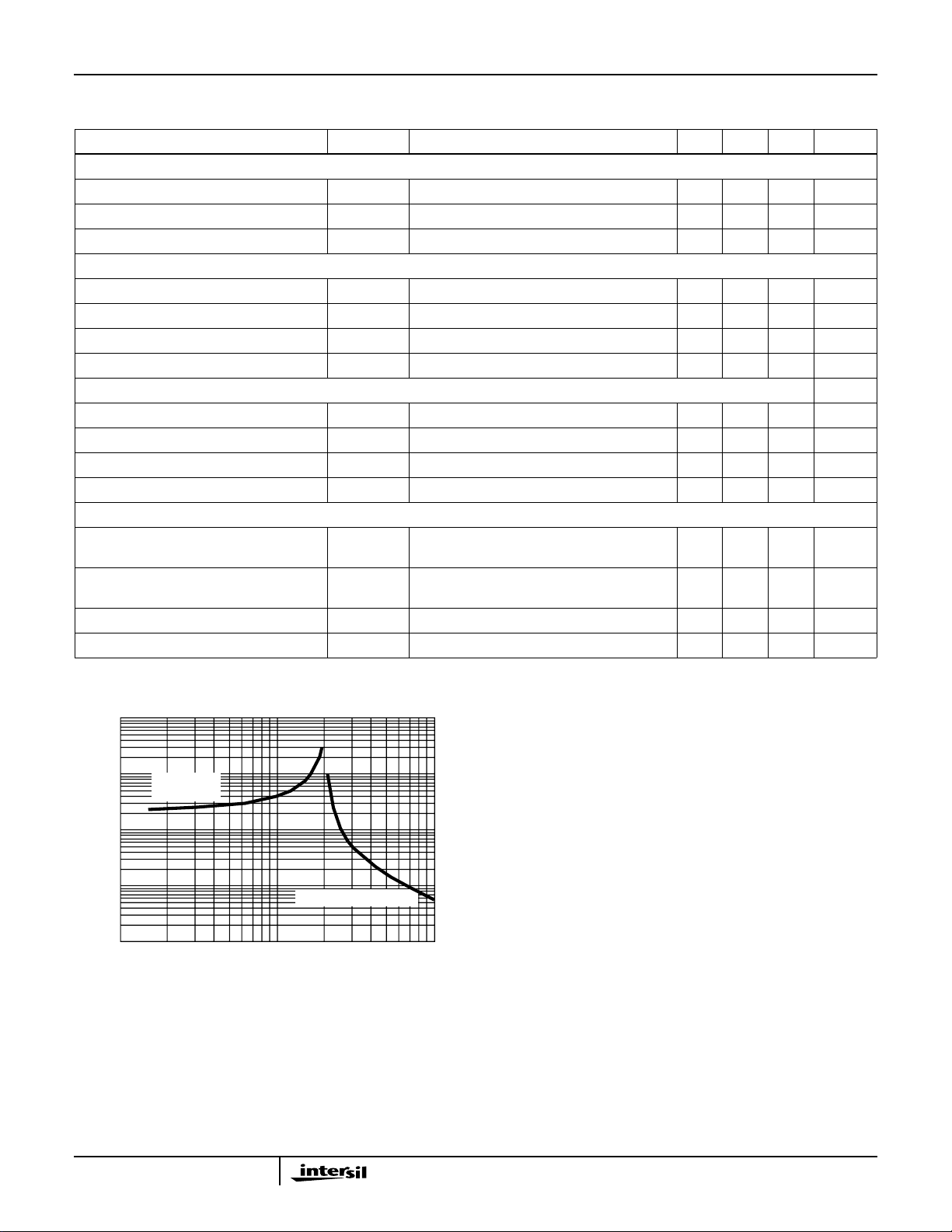
Typical Performance Curve
1000
100
RESISTANCE (kΩ)
10
RT PULLUP
TO +12V
RT PULLDOWN TO V
10 100 1000
SWITCHING FREQUENCY (kHz)
FIGURE 1. RT RESISTANCE vs FREQUENCY
SS
5

HIP6021A
Functional Pin Descriptions
VCC (Pin 28)
Provide a 12V bias supply for the IC to this pin. This pin also
provides the gate bias charge for all the MOSFETs
controlled by the IC. The voltage at this pin is monitored for
Power-On Reset (POR) purposes.
GND (Pin 17)
Signal ground for theIC. All voltage levelsare measured with
respect to this pin.
PGND (Pin 24)
This is the power ground connection. Tie the synchronous
PWM converter’s lower MOSFET source to this pin.
VAUX (Pin 16)
This pin provides boost current for the linear regulators’
output drives in the event bipolar NPN transistors (instead
of N-Channel MOSFETs) are employed as pass elements.
The voltage at this pin is monitored for power-on reset
(POR) purposes.
SS (Pin 12)
Connect a capacitor from this pin to ground. This capacitor,
along with an internal 28µA current source, sets the softstart
interval of the converter.
FAULT / RT (Pin 13)
This pin provides oscillator switching frequency adjustment.
By placing a resistor (R
200kHz switching frequency is increased according to the
following equation:
510
Fs 200kHz
×
-------------------- -+≈
RTkΩ()
Conversely, connecting a resistor from this pin to VCC
reduces the switching frequency according to the following
equation:
410
Fs 200kHz
×
-------------------- -–≈
RTkΩ()
Nominally, the voltage at this pin is 1.26V. In the event of an
over-voltage or over-current condition, this pin is internally
pulled to VCC.
PGOOD (Pin 8)
PGOOD is an open collector output used to indicate the
status of the output voltages. This pin is pulled low when the
synchronous regulator output is not within ±10% of the
DACOUT referencevoltage or when any of the other outputs
are below their under-voltage thresholds.
The PGOOD output is open for ‘11111’ VID code.
SD (Pin 9)
This pin shuts down all the outputs. A TTL-compatible, logic
level high signal applied at this pin immediately discharges
) from this pin to GND, the nominal
T
6
(RT to GND)
7
(R
to 12V)
T
the soft-start capacitor, disabling all the outputs. Dedicated
internal circuitry insures the core output voltage does not go
negative during this process. When re-enabled, the IC
undergoes a new soft-start cycle. Left open, this pin is pulled
low by an internal pull-down resistor, enabling operation.
FIX (Pin 2)
Grounding this pin bypasses the internal resistor dividers
that set the output voltage of the 1.5V and 1.8V linear
regulators. This way, the output voltage of the two regulators
can be adjusted from 1.26V up to the input voltage (+3.3V or
+5V) by way of an external resistor divider connected at the
corresponding VSEN pin. The new output voltage set by the
external resistor divider can be determined using the
following formula:
R
1.265V 1
V
OUT
where R
×=
is the resistor connected from VSEN to the
OUT
output of the regulator, and R
OUT
---------------- -+
R
GND
is the resistor connected
GND
from VSEN to ground. Left open, the FIX pin is pulled high,
enabling fixed output voltage operation.
VID0, VID1, VID2, VID3, VID4 (Pins 7, 6, 5, 4 and 3)
VID0-4 are the TTL-compatible input pins to the 5-bit DAC.
The logic states of these five pins program the internal
voltage reference (DACOUT).The level of DACOUT sets the
microprocessor core converter output voltage, as well as the
corresponding PGOOD and OVP thresholds.
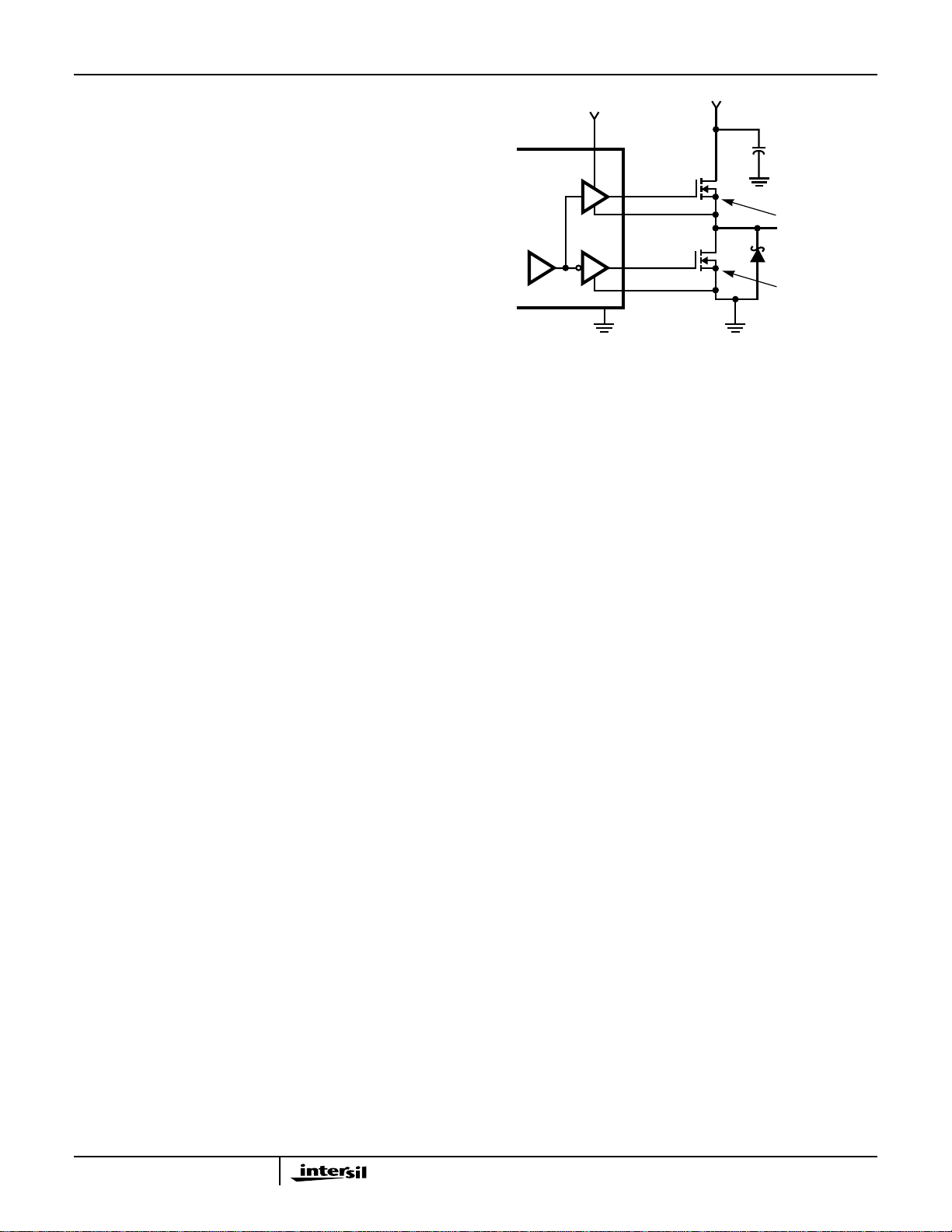
OCSET (Pin 23)
Connect a resistor from this pin to the drain of the respective
upper MOSFET. This resistor, an internal 200µA current
source, and the upper MOSFET’s on-resistance set the
converter over-current trip point. An over-current trip cycles
the soft-start function.
The voltage at this pin is monitored for power-on reset (POR)
purposes and pulling this pin low with an open drain device
will shutdown the IC.
PHASE (Pin 26)
Connect the PHASE pin to the PWM converter’s upper
MOSFET source. This pin represents the gate drive return
current path and is used to monitor the voltage drop across
the upper MOSFET for over-current protection.
UGATE (Pin 27)
Connect UGATEpin to the PWM converter’supper MOSFET
gate. This pin provides the gate drive for the upper MOSFET.
LGATE (Pin 25)
Connect LGATE to the PWM converter’s lower MOSFET
gate. This pin provides the gate drive for the lower MOSFET.
COMP and FB (Pin 20 and 21)
COMP and FB are the available external pins of the PWM
converter error amplifier. The FB pin is the inverting input of the
6

HIP6021A
error amplifier. Similarly, the COMP pin is the error amplifier
output. These pins are used to compensate the voltage-mode
control feedback loop of the synchronous PWM conv erter .
VSEN1 (Pin 22)
This pin is connected to the PWM converter’s output voltage.
The PGOOD and OVP comparator circuits use this signal to
report output voltage status and for over-voltage protection.
DRIVE2 (Pin 1)
Connect this pin to the gate of an external MOSFET. This pin
provides the drive for the AGP regulator’s pass transistor.
VSEN2 (Pin 10)
Connect this pin to the output of the AGP linear regulator.
The voltage at this pin is regulated to the level
predetermined by the logic-level status of the SELECT pin.
This pin is also monitored for under-voltage events.
SELECT (Pin 11)
This pin determines the output voltageof the AGP bus linear
regulator. A low TTL input sets the output voltage to 1.5V
and the linear controller regulates this voltage to within ±3%.
A TTL high input turns Q3 on continuously, providing a DC
current path from the input (+3.3V
of the AGP controller.
) to the output (V
IN
OUT2
DRIVE3 (Pin 18)
Connect this pin to the gate of an external MOSFET. This pin
provides the drive for the 1.5V regulator’s pass transistor.
VSEN3 (Pin 19)
Connect this pin to the output of the 1.5V linear regulator.
This pin is monitored for under-voltage events.
DRIVE4 (Pin 15)
Connect this pin to the gate of an external MOSFET. This pin
provides the drive for the 1.8V regulator’s pass transistor.
VSEN4 (Pin 14)
Connect this pin to the output of the linear 1.8V regulator.
This pin is monitored for under voltage events.
Description
Operation
The HIP6021A monitors and precisely controls 4 output
voltage levels (Refer to Block and Simplified Power System
Diagrams,and Typical ApplicationSchematic). It is designed
for microprocessor computer applications with 3.3V, 5V,
and 12V bias input from an ATX power supply. The
microprocessor core voltage (V
synchronous-rectified buck converter configuration. The
PWM controller regulates the microprocessor core voltage
to a level programmed by the 5-bit digital-to-analog
converter (DAC).
) is controlled in a
OUT1
The AGPbus voltage(VOUT2) is set using the SELECT pin
to either a 1.5V linear regulated output or to the 3.3V
through a pass device. Selection of either output voltage is
set depending on the logic level of the SELECT pin.
The two remaining linear controllers supply the 1.5V GTL
bus power (V
These output voltages are user adjustable. All linear
controllers are designed to employ an external pass
transistor.
) and the 1.8V memory power (V
OUT3
IN
OUT4
).
Initialization
The HIP6021A automatically initializes upon receipt of input
power. Special sequencing of the input supplies is not
necessary. The Power-On Reset (POR) function continually
monitors the input supply voltages. The POR monitors the
bias voltage (+12V
(+5V
) on the OCSET pin, and the 3.3V input voltage
IN
(+3.3V
equal to +5V
protection). The POR function initiates soft-start operation
after all supply voltages exceed their POR thresholds.
) at the VAUX pin. The normal level on OCSET is
IN
IN
) at the VCC pin, the 5V input voltage
IN
less a fixed voltage drop (see over-current
Soft-Start
)
The POR function initiates the soft-start sequence. Initially,
the voltage on the SS pin rapidly increases to approximately
1V (this minimizes the softstart interval). Then an internal
28µA current source charges an external capacitor (C
the SS pin to 4.5V. The PWM error amplifier reference input
(+ terminal) and output (COMP pin) are clamped to a level
proportional to the SS pin voltage. As the SS pin voltage
slews from 1V to 4V, the output clamp allows generation of
PHASE pulses of increasing width that charge the output
capacitor(s). After the output voltage increases to
approximately 70% of the set value, the reference input
clamp slows the output voltage rate-of-rise and provides a
smooth transition to the final set voltage. Additionally, all
linear regulators’ reference inputs are clamped to a voltage
proportional to the SS pin voltage. This method provides a
rapid and controlled output voltage rise.
Figure 2 shows the soft-start sequence for the typical
application. At T0 the SS voltage rapidly increases to
approximately 1V. At T1, the SS pin and error amplifier
output voltage reach the valley of the oscillator’s triangle
wave. The oscillator’s triangular waveform is compared to
the clamped error amplifier output voltage. As the SS pin
voltage increases, the pulse width on the PHASE pin
increases. The interval of increasing pulse width continues
until each output reaches sufficient voltage to transfer
control to the input reference clamp. If we consider the 2.5V
core output (V
During the interval between T2 and T3, the error amplifier
reference ramps to the final value and the converter
regulates the output a voltage proportional to the SS pin
voltage. At T3 the input clamp voltage exceeds the
reference voltage and the output voltage is in regulation.
) in Figure 2, this time occurs at T2.
OUT1
SS
)on
7

0V
0V
VOLTAGES
0V
PGOOD
SOFT-START
(1V/DIV)
V
OUT2
V
OUT1
V
OUT4
OUTPUT
(0.5V/DIV)
T1 T2 T3T0 T4
FIGURE 2. SOFT-START INTERVAL
TIME
V
OUT3
(= 3.3VIN)
(DAC = 2.5V)
(= 1.8V)
(= 1.5V)
The remaining outputs are also programmed to follow the
SS pin voltage. The PGOOD signal toggles ‘high’ when all
output voltage levels have exceeded their under-voltage
levels.The waveform for V
represents the case where
OUT2
SELECT is held ‘high’. The AGPbus voltage is controlled in
the same manner as the other linear regulators during the
softstart sequence. Once the softstart sequence is
complete (T4), the gate of the external pass device is fully
enhanced and V
tracks the 3.3VIN voltage. See the
OUT2
Soft-Start Interval sectionunder Applications Guidelines for
a procedure to determine the soft-start interval.
HIP6021A
Over-Voltage Protection
During operation,a short on the upper MOSFET of the PWM
regulator (Q1) causes V
exceedsthe over-voltagethreshold of 115% of DACOUT, the
over-voltage comparator trips to set the fault latch and turns
Q2 on. This blows the input fuse and reduces V
fault latch raises the FAULT/RT pin to VCC.
A separate over-voltage circuit provides protection during
the initial application of power. For voltages on the VCC pin
below the power-on reset (and above ~4V), the output level
is monitored for voltages above1.3V. Should VSEN1 exceed
this level, the lower MOSFET, Q2 is driven on.
Over-Current Protection
All outputs are protected against excessive over-currents.
The PWM controller uses the upper MOSFET’s
on-resistance, r
against shorted output. All linear controllers monitor their
respective VSEN pins for under-voltage events to protect
against excessive currents.
LUV
OVER-
CURRENT
LATCH
OC1
0.15V
+
-
SS
OV
+
-
4V
FIGURE 3. FAULT LOGIC - SIMPLIFIED SCHEMATIC
SRQ
COUNTER
R
UP
POR
to increase. When the output
OUT1
to monitor the current for protection
DS(ON)
INHIBIT
FAULT
LATCH
SRQ
OUT1
VCC
FAULT
. The
Fault Protection
All four outputs aremonitored and protected against extreme
overload. A sustained overload on any output or an overvoltage on V
drives the FAULT/RT pin to VCC.
Figure 3 shows a simplified schematic of the fault logic. An
over-voltage detected on VSEN1 immediately sets the fault
latch. A sequence of three over-current fault signals also
sets the fault latch. The over-current latch is set dependent
upon the states of the over-current (OC), linear undervoltage (LUV) and the soft-start signals. A window
comparator monitors the SS pin and indicates when C
fully charged to 4V (UP signal). An under-voltage on either
linear output (VSEN2, VSEN3, or VSEN4) is ignored until
after the soft-start interval (T4 in Figure 2). This allows
V
OUT2,VOUT3
up.Cycling the bias input voltage (+12V
then on) resets the counter and the fault latch.
output (VSEN1) disables all outputs and
OUT1
, and V
to increase without fault at start-
OUT4
on theVCC pin off
IN
8
SS
is
Figure 4 illustrates the over-current protection with an
overload on OUT1. The overload is applied at T0 and the
current increases through the inductor (L
). At time T1,
OUT1
the OVER-CURRENT comparator trips when the voltage
across Q1 (i
D•rDS(ON)
) exceeds the level programmed by
ROCSET. This inhibits all outputs, discharges the soft-start
capacitor (C
the counter. C
) with a 10mA current sink, and increments
SS
recharges at T2 and initiates a soft-start
SS
cycle with the error amplifiers clamped by soft-start. With
OUT1 still overloaded, the inductor current increases to trip
the over-current comparator. Again, this inhibits all outputs,
but the soft-start voltage continues increasing to 4V before
discharging. The counter increments to 2. The soft-start
cycle repeats at T3 and trips the over-current comparator.
The SS pin voltage increases to 4V at T4 and the counter
increments to 3. This sets the fault latch to disable the
converter. The fault is reported on the FAULT/RT pin.
The linear controllers operate in the same way as the PWM
in response to over-current faults. The differentiating factor

HIP6021A
for the linear controllers is that they monitor the VSEN pins
for under-voltage events. Should excessive currents cause
the voltage at the VSEN pins to fall below the linear undervoltage threshold, the LUV signal sets the over-current
latch if C
the C
is fully charged. Blanking the LUV signal during
SS
charge interval allows the linear outputs to build
SS
abovethe under-voltagethreshold during normal operation.
Cycling the bias input power off then on resets the counter
and the fault latch.
FAULT
10V
0V
FAULT/RT
4V
2V
0V
0A
INDUCTOR CURRENT SOFT-START
FIGURE 4. OVER-CURRENT OPERATION
A resistor (R
COUNT
= 1
OVERLOAD
APPLIED
T1 T2 T3T0 T4
) programs the over-current trip levelfor
OCSET
REPORTED
COUNT
= 2
TIME
COUNT
= 3
the PWM converter. As shown in Figure 5, the internal
200µA current sink, I
R
OCSET(VSET
) that is referenced to VIN. The DRIVE
develops a voltage across
OCSET
signal enables the over-current comparator (OVERCURRENT). When the voltage across the upper MOSFET
(V
) exceeds V
DS
set the over-current latch. Both V
referenced to V
helps V
OCSET
, the over-current comparator trips to
SET
and a small capacitor across R
IN
and VDS are
SET
OCSET
track the variations of VIN due to MOSFET
switching. The over-current function will trip at a peak
inductor current (I
I
OCSETROCSET
I
PEAK
--------------------------------------------------- -
=
r
DS ON()
×
determined by:
PEAK)
OVER-CURRENT TRIP:
VDSV
>
× I
iDr
DS ON()
OVER-
CURRENT
OC
PWM
SET
×>
OCSETROCSET
R
OCSET
I
OCSET
200µA
DRIVE
+
-
GATE
CONTROL
FIGURE 5. OVER-CURRENT DETECTION
OCSET
V
VCC
UGATE
PHASE
V
PHASEVINVDS
V
OCSETVINVSET
The OC trip point varies with MOSFET’s r
SET
VIN = +5V
i
+
DS(ON)
D
+
V
DS
–=
–=
temperature variations.Toavoid over-currenttripping in the
normal operating load range, determine the R
OCSET
resistor from the equation above with:
1. The maximum r
2. The minimum I
3. Determine I
PEAK
DS(ON)
OCSET
at the highest junction temperature.
from the specification table.
for I
PEAK>IOUT(MAX)
+(∆I)/2, where
∆I is the output inductor ripple current.
For an equation for the ripple current see the section under
component guidelines titled ‘PWM Output Inductor
Selection’.
OUT1 Voltage Program
The output voltage of the PWM converter is programmed to
discrete levels between 1.3V
(OUT1) is designed to supply the core voltage of Intel’s
advanced microprocessors. The voltage identification (VID)
pins programan internal voltage reference(DACOUT) with a
TTL-compatible 5-bit digital-to-analog converter. The level of
DACOUT also sets the PGOOD and OVP thresholds.
Table 1 specifies the DACOUT voltage for the different
combinations of connections on the VID pins. The VID pins
can be left open for a logic 1 input, because they are
internally pulled up to an internal voltage of about 5V by a
10µA current source. Changing the VID inputs during
operation is not recommended and could toggle the PGOOD
signal and exercise the over-voltage protection.
and 3.5VDC. This output
DC
9

HIP6021A
TABLE 1. OUT1 VOLTAGE PROGRAM
PIN NAME NOMINAL
DACOUT
VOLTAGEVID4 VID3 VID2 VID1 VID0
011111.30
011101.35
011011.40
011001.45
010111.50
010101.55
010011.60
010001.65
001111.70
001101.75
001011.80
001001.85
000111.90
000101.95
000012.00
000002.05
111112.00
111102.1
111012.2
111002.3
110112.4
110102.5
110012.6
110002.7
101112.8
101102.9
101013.0
101003.1
100113.2
100103.3
100013.4
100003.5
NOTE: 0 = connected to GND,1 = open or connected to 5V through
pull-up resistors.
OUT2 Voltage Selection
The AGP output voltage is internally set to one of two levels,
based on the status of the SELECT pin. Grounding the
SELECT pin enables the internal 1.5V regulator control
circuitry.Left open, the SELECT pin is internally pulled ‘high’
and the AGPvoltage is regulated to 3.3V during the softstart
sequence. Once complete, the gate drive is increased and
the regulator becomes a simple pass circuit for the 3.3V
input voltage.
OUT3 and OUT4 Voltage Adjustability
The GTL bus voltage (1.5V, OUT3) and the chip set and/or
cache memory voltage (1.8V, OUT4) are internally set for
simple, low-cost implementation in typical Intel motherboard
architectures. However, if different voltage settings are
desired for these two outputs, the FIX pin provides the
necessary adaptability. Left open (NC), this pin sets the fixed
output voltages described above. Grounding this pin allows
both output voltages to be set by means of external resistor
dividers as shown in Figure 6.
R
R
--------+
R
P3
S
P
VAUX
DRIVE3
VSEN3
HIP6021A
DRIVE4
VSEN4
FIX
+3.3V
IN
Q4
V
OUT3
R
C
OUT3
Q5
V
OUT4
C
OUT4
V
OUTVBG
FIGURE 6. ADJUSTING THE OUTPUT VOLTAGE OF
OUTPUTS 3 AND 4
S3
R
S4
R
P4
1
×=
Application Guidelines
Soft-Start Interval
Initially, the soft-start function clamps the error amplifier’s
output of the PWM converter. This generatesPHASE pulses
of increasing width that charge the output capacitor(s). After
the output voltage increases to approximately70% of the set
value, the reference input of the error amplifier is clamped to
a voltage proportional to the SS pin voltage. The resulting
output voltages start-up as shown in Figure 2.
The soft-start function controls the output voltage rate of rise
to limitthe current surge atstart-up. The soft-start interval and
the surge current are programmed by the soft-start capacitor,
C
. Programming a faster soft-start interval increases the
SS
peak surge current. The peak surge current occurs during the
initial output voltage rise to 70% of the set value.
10

HIP6021A
Shutdown
The HIP6021A features a dedicated shutdown pin (SD). A
TTL-compatible, logic high signal applied to this pin shuts
down (disables) all four outputs and discharges the soft-start
capacitor. Following a shutdown, a logic low signal
re-enables the outputs through initiation of a new soft-start
cycle. Left open this pin willasses a logic lowstate, due to its
internal pull-down resistor, thus enabling normal operation of
all outputs.
The PWM output does not switch until the soft-start voltage
(V
) exceeds the oscillator’s valley voltage. The references
SS
on each linear’s error amplifier are clamped to the soft-start
voltage. Holding the SS pin low (with an open drain or
collector signal) turns off all four regulators.
The ‘11111’ VID code also shuts down the IC.
Layout Considerations
MOSFETs switch very fast and efficiently. The speed with
which the current transitions from one device to another
causes voltage spikes across the interconnecting
impedances and parasitic circuit elements. The voltage
spikes can degrade efficiency, radiate noise into the circuit,
and lead to device over-voltage stress. Careful component
layout and printed circuit design minimizes the voltage
spikes in the converter. Consider, as an example, the turnoff transition of the upper PWM MOSFET. Prior to turn-off,
the upper MOSFET was carrying the full load current.
During the turn-off, current stops flowing in the upper
MOSFET and is picked up by the lower MOSFET or
Schottky diode. Any inductance in the switched current
path generates a large voltage spike during the switching
interval. Careful component selection, tight layout of the
critical components, and short, wide circuit traces minimize
the magnitude of voltage spikes. See Application Note
AN9836 for evaluation board drawings of the component
placement and the printed circuit board layout of a typical
application.
There are two sets of critical components in a DC-DC
converter using a HIP6021A controller. The switching power
components are the most critical because they switch large
amounts of energy, and as such, they tend to generate
equally large amounts of noise. The critical small signal
components are those connected to sensitive nodes or
those supplying critical bypass current.
The power components and the controller IC should be
placed first. Locate the input capacitors, especially the highfrequency ceramicdecoupling capacitors, closeto the power
switches. Locate the output inductor and output capacitors
between the MOSFETs and the load. Locate the PWM
controller close to the MOSFETs.
The critical small signal components include the bypass
capacitor for VCC and the soft-start capacitor, C
these components close to their connecting pins on the
. Locate
SS
control IC. Minimize any leakage current paths from SS
node, since the internal current source is only 28µA.
A multi-layer printed circuit board is recommended.
Figure 7 shows the connections of the critical components
in the converter. Note that the capacitors C
and C
IN
OUT
each represent numerous physical capacitors. Dedicate
one solid layer for a ground plane and make all critical
component ground connections with vias to this layer.
Dedicate another solid layer as a power plane and break
this plane into smaller islands of common voltage levels.
The power plane should support the input power and
output power nodes. Use copper filled polygons on the top
and bottom circuit layers for the PHASE nodes, but do not
unnecessarily oversize these particular islands. Since the
PHASE nodes are subjected to very high dV/dt voltages,
the stray capacitor formed between these islands and the
surrounding circuitry will tend to couple switching noise.
Use the remaining printed circuit layers for small signal
wiring. The wiring traces from the control IC to the
MOSFET gate and source should be sized to carry 2A
peak currents.
PWM Controller Feedback Compensation
The PWM controller uses voltage-mode control for output
regulation. This section highlights the design consideration
for a PWM voltage-mode controller. Apply the methods and
considerations only to the PWM controller.
Figure 8 highlights the voltage-mode control loop for a
synchronous-rectified buck converter. The output voltage
(V
) is regulated to the Reference voltage level. The
OUT
referencevoltage levelis the DACoutput voltage(DACOUT).
The error amplifier (Error Amp) output (V
) is compared
E/A
with the oscillator (OSC) triangular wave to provide a pulsewidth modulated (PWM) wave with an amplitude of V
IN
at
the PHASE node. The PWM waveis smoothed bythe output
filter (L
and CO).
O
The modulator transfer function is the small-signal transfer
function of V
OUT/VE/A
Gain, given by V
with a double pole break frequency at F
at F
ESR
.
. This function is dominated by a DC
IN/VOSC
, and shaped by the output filter,
and a zero
LC
Modulator Break Frequency Equations
--------------------------------------- -=
2π L
1
××
OCO
F
ESR
F
LC
The compensation network consists of the error amplifier
(internal to the HIP6021A) and the impedance networks Z
and ZFB. Thegoal of the compensation network is to provide
a closed loop transfer function with high 0dB crossing
frequency (f
) and adequate phase margin. Phase margin
0dB
is the difference between the closed loop phase at f
180 degrees. The equations below relate the compensation
network’spoles, zeros and gain to the components (R1, R2,
-----------------------------------------=
2π ESR CO××
1
and
0dB
IN
11

HIP6021A
R3, C1, C2, and C3) in Figure 7. Use these guidelines for
locating the poles and zeros of the compensation network:
1. Pick Gain (R2/R1) for desired converter bandwidth
ST
2. Place 1
3. Place 2
4. Place 1
5. Place 2
Zero Below Filter’s Double Pole (~75% FLC)
ND
Zero at Filter’s Double Pole
ST
Pole at the ESR Zero
ND
Pole at Half the Switching Frequency
6. Check Gain against Error Amplifier’s Open-Loop Gain
7. Estimate Phase Margin - Repeat if Necessary
L
IN
IN
OUT2
LOAD
OUT3
LOAD
+3.3V
IN
C
C
IN
C
IN
OUT2
OUT3
Q3
C
Q4
SS
+12V
C
VCC
GNDVCC
OCSET1
DRIVE2
UGATE1
PHASE1
LGATE1
SS
HIP6021A
DRIVE4
DRIVE3
PGND
KEY
ISLAND ON POWER PLANE LAYER
ISLAND ON CIRCUIT PLANE LAYER
VIA CONNECTION TO GROUND PLANE
C
OCSET1
Q2
Q5
R
OCSET1
Q1
L
OUT1
C
OUT1
CR1
C
OUT4
V
V
OUT1
OUT4
LOAD
+5V
+3.3V
V
V
FIGURE 7. PRINTED CIRCUIT BOARDPOWER PLANES AND
ISLANDS
Figure 9 shows an asymptotic plot of the DC-DC converter’s
gain vs frequency. The actual Modulator Gain has a high gain
peak dependent on the quality factor (Q) of the output filter ,
which is not shown in Figure 8. Using the above guidelines
should yield a Compensation Gain similar to the curve plotted.
The gain. Check the compensation gain at F
with the
P2
capabilities of the error amplifier. The Closed Loop Gain is
constructed on the log-log graph of Figure 9 by adding the
Modulator Gain (in dB) to the Compensation Gain (in dB). This
isequivalent tomultiplying themodulator transferfunctionto the
compensation transfer function and plotting the gain.
The compensation gain uses external impedance networks
Z
and ZINto providea stable,high bandwidth (BW) overall
FB
loop. A stable control loop has a gain crossing with
-20dB/decade slope and a phase margin greater than 45
degrees. Include worst case component variations when
determining phase margin.
LOAD
V
FB
Z
FB
IN
L
O
PHASE
(PARASITIC)
Z
IN
C3
R1
C
ESR
R3
V
OUT
O
V
OUT
∆V
OSC
OSC
PWM
COMP
-
+
Z
FB
V
E/A
-
+
ERROR
AMP
DETAILED COMPENSATION COMPONENTS
COMP
DRIVER
DRIVER
REFERENCE
C2
C1
R2
Z
IN
-
+
HIP6021A
DACOUT
FIGURE 8. VOLTAGE-MODEBUCK CONVERTER
COMPENSATION DESIGN
Compensation Break Frequency Equations
F
Z1
F
Z2
100
80
60
40
20
GAIN (dB)
0
-20
-40
-60
1
-----------------------------------=
2π R× 2C1×
------------------------------------------------------ -=
2π R1 R3+()C3××
F
R2
20
log
------- -
R1
MODULATOR
GAIN
1
Z1
F
Z2
FLCF
ESR
FREQUENCY (Hz)
F
F
F
P1
P2
P1
-------------------------------------------------------=
2π R
-----------------------------------=
2π R× 3C3×
F
P2
FIGURE 9. ASYMPTOTIC BODE PLOT OF CONVERTER GAIN
1
C1 C2×
----------------------
××
2
C1 C2+
1
OPEN LOOP
ERROR AMP GAIN
V
20
log
------------
V
COMPENSATION
GAIN
CLOSED LOOP
GAIN
10M1M100K10K1K10010
IN
PP
12

HIP6021A
Component Selection Guidelines
Output Capacitors
The output capacitors for each output have unique
requirements. In general, the output capacitors should be
selected to meet the dynamic regulation requirements.
Additionally,the PWM convertersrequire an output capacitor
to filter the current ripple. The load transient for the
microprocessor core requires high quality capacitors to
supply the high slew rate (di/dt) current demands.
PWM Output
Modern microprocessors produce transientload rates above
1A/ns. High frequency capacitors initially supply the
transient current and slow the load rate-of-change seen by
the bulk capacitors. The bulk filter capacitor values are
generally determined by the ESR (effective series
resistance) and voltage rating requirements rather than
actual capacitance requirements.
High frequency decoupling capacitors should be placed as
close to the power pins of the load as physically possible. Be
careful not to add inductance in the circuit board wiring that
could cancel the usefulness of these low inductance
components. Consult with the manufacturer of the load on
specific decoupling requirements.
Use only specialized low-ESR capacitors intended for
switching-regulator applications for the b ulk capacitors. The
bulk capacitor’s ESR determines the output ripple voltage and
the initial voltage drop following a high slew-rate transient’ s
edge. An aluminum electrolytic capacitor’ s ESR value is
related to the case size with lower ESR available in larger
case sizes. However , the equivalent series inductance (ESL)
of these capacitors increases with case size and can reduce
the usefulness of the capacitor to high slew-rate transient
loading. Unfortunately,ESL is not a specifiedparameter.Work
with your capacitor supplier and measure the capacitor’s
impedance with frequency to select a suitable component. In
most cases, multiple electrolytic capacitors of small case size
perform better than a single large case capacitor.
Linear Output Capacitors
The output capacitors for the linear regulators provide
dynamic load current. The linear controllers use dominant
pole compensation integrated into the error amplifier and are
insensitive to output capacitor selection. Output capacitors
should be selected for transient load regulation.
PWM Output Inductor
The PWM converter requires an output inductor. The output
inductor is selected to meet the output voltage ripple
requirements and sets the converter’s response time to a
load transient. The inductor value determines the converter’s
ripple current and the ripple voltage is a function of the ripple
current. The ripple voltage and current are approximated by
the following equations:
∆I
VINV
–
------------------------------- -
F
S
OUT
L×
V
--------------- -
×=
OUT
V
IN
∆ I∆ ESR×=
V
OUT
Increasing thevalue of inductance reduces the ripple current
and voltage. However, the large inductance values increase
the converter’s response time to a load transient.
One of the parameters limiting the converter’s response to a
load transient is the time required to change the inductor
current. Given a sufficiently fast control loop design, the
HIP6021A will provide either 0% or 100% duty cycle in
response to a load transient. The response time is the time
interval required to slew the inductor current from an initial
current value to the post-transient current level. During this
interval the difference between the inductor current and the
transient current level must be supplied by the output
capacitor(s). Minimizing the response time can minimize the
output capacitance required.
The response time to a transient is different for the
application of load and the removal of load. The following
equations give the approximate response time interval for
application and removal of a transient load:
LOI
×
TRAN
t
RISE
where: I
------------------------------- -=
–
V
INVOUT
is the transient load current step, t
TRAN
t
FALL
response time to the application of load, and t
LOI
×
------------------------------ -=
V
TRAN
OUT
RISE
FALL
is the
is the
response time to the removal of load. Be sure to check both
of these equations at the minimum and maximum output
levels for the worst case response time.
Input Capacitors
The important parameters for the bulk input capacitors are
the voltage rating and the RMS current rating. For reliable
operation, select bulk input capacitors with voltage and
current ratingsabove the maximum input voltage and largest
RMS current required by the circuit. The capacitor voltage
rating should be at least 1.25 times greater than the
maximum input voltage and a voltage rating of 1.5 times is a
conservative guideline. The RMS current rating requirement
for the input capacitor of a buck regulator is approximately
1/2 of the summation of the DC load current.
Use a mix of input bypass capacitors to control the voltage
overshoot across the MOSFETs. Use ceramic capacitance
for the high frequency decoupling and bulk capacitors to
supply the RMS current. Small ceramic capacitors can be
placed very close to the upper MOSFET to suppress the
voltage induced in the parasitic circuit impedances.
For a through-hole design, sev er al electrolytic capacitors
(PanasonicHFQ series or NichiconPL series or SanyoMV-GX
or equivalent) maybe needed. Forsurface mount designs, solid
tantalum capacitors can be used, but caution must be
exercised with regard to the capacitor surge current rating.
These capacitors must be capable of handling the surgecurrent at power-up. The TPS series av ailab le from AVX, and
the 593D series from Sprague are both surge current tested.
13
HIP6021A
MOSFET Considerations
The HIP6021A requires 5 external transistors. TwoN-Channel
MOSFETs are used in the synchronous-rectified buck
topology of PWM1 converter. It is recommended that the
AGP linear regulator pass element be a N-Channel
MOSFET as well. The GTL and memory linear controllers
can also each drive a MOSFET or a NPN bipolar as a pass
transistor. All these transistors should be selected based
upon r
DS(ON)
, current gain, saturation voltages, gate supply
requirements, and thermal management considerations.
PWM MOSFETs
In high-current PWM applications, the MOSFET power
dissipation, package selection and heatsink are the
dominant design factors.The power dissipation includes two
loss components; conduction loss and switching loss. These
losses are distributed between the upper and lower
MOSFETs according to duty factor (see the equations
below). The conduction losses are the main component of
power dissipation for the lower MOSFETs. Only the upper
MOSFET has significant switching losses, since the lower
device turns on and off into near zero voltage.
The equations below assume linear voltage-current
transitions and do not model power loss due to the reverserecovery of the lower MOSFET’s body diode. The gatecharge losses are dissipated by the HIP6021A and don't
heat the MOSFETs. However, large gate-charge increases
the switching time, t
switchinglosses. Ensure thatboth MOSFETs are withintheir
maximum junction temperature at high ambient temperature
by calculating the temperature rise according to package
thermal-resistance specifications. A separate heatsink may
be necessary depending upon MOSFET power, package
type, ambient temperature and air flow.
2
I
× V
P
UPPER
P
LOWER
The r
O
------------------------------------------------------------
2
I
× VINV
O
-------------------------------------------------------------------------------- -=
is different for the two equations above even if
DS(ON)
the same device is used for both. This is because the gate
drive applied to the upper MOSFET is different than the
lower MOSFET. Figure 10 shows the gate drive where the
upper MOSFET’s gate-to-source voltage is approximately
VCC less the input supply. For +5Vmain power and +12VDC
for the bias, the gate-to-source voltage of Q1 is 7V. The
lowergate drive voltageis +12VDC.A logic-levelMOSFET is
a good choice for Q1 and a logic-levelMOSFET can be used
for Q2 if its absolute gate-to-source voltage rating exceeds
the maximum voltage applied to VCC.
which increases the upper MOSFET
SW
r
r
×
DS ON()
V
IN
DS ON()
V
IN
OUT
× tSW× FS×
I
OVIN
----------------------------------------------------+=
–()×
OUT
2
+12V
VCC
+5V OR LESS
HIP6021A
UGATE
PHASE
-
+
IGURE 10. UPPER GATE DRIVE - DIRECT VCC DRIVE OPTION
LGATE
PGND
GND
Q1
Q2
CR1
NOTE:
V
GS
NOTE:
V
GS
≈ V
≈ V
CC
CC
-5V
Rectifier CR1 is a clamp that catches the negative inductor
swing during the dead time between the turn off of the lower
MOSFET and the turn on of the upper MOSFET. The diode
must be a Schottky type to prevent the lossy parasitic
MOSFET body diode from conducting. It is acceptable to
omit the diode and let the body diode of the lower MOSFET
clamp the negative inductor swing, but efficiency could drop
one or two percent as a result. The diode's rated reverse
breakdown voltage must be greater than the maximum input
voltage.
Linear Controller Transistors
The main criteria for selection of transistors for the linear
regulators is package selection for efficient removal of heat.
The power dissipated in a linear regulator is:
P
LINEARIOVINVOUT
Select a package and heatsink that maintains the junction
temperature below the rating with a the maximum expected
ambient temperature.
When selecting bipolar NPN transistors for use with the
linear controllers, insure the current gain at the given
operating VCE is sufficiently large to provide the desired
output load current when the base is fed with the minimum
driver output current.
–()×=
14

HIP6021A
HIP6021A DC-DC Converter Application Circuit
Figure 11 shows an application circuit of a power supply for a
microprocessor computer system. The power supply provides
the microprocessor core voltage (VOUT1), the AGP bus
voltage (VOUT2), the GTL b us v oltage (VOUT3), and the
memory voltage (VOUT4) from +3.3V, +5VDC, and +12VDC.
+12V
IN
L1
+5V
GND
+3.3V
IN
IN
1µH
C1-6
6x1000µF
FAULT/RT
+
VAUX
VCC
28
13
16
For detailed information on the circuit, including a Bill-ofMaterials and circuit board description, see Application Note
AN9836. Also see Intersil’s web page (http://www.intersil.com)
or Intersil AnswerF AX(407-724-7800) Document No. 99836 for
the latest information.
C7
1µF
23
8
OCSET
PGOOD
C8
1000pF
R1
1.0K
C9
1µF
POWERGOOD
V
OUT2
(3.3VIN OR 1.5V)
TYPEDET
HUF76107D3S
V
OUT3
(1.5V)
V
OUT4
(1.8V)
+
C10, 11
2x1000µF
Q4
+
C23, 24
2x1000µF
HUF76107D3S
+
C25, 26
2x1000µF
Q5
Q3
HUF76121D3S
DRIVE2
VSEN2
SELECT
DRIVE3
VSEN3
DRIVE4
VSEN4
SD
FIX
1
10
11
18
19
15
14
9
2
U1
HIP6021A
17
GND
27
26
25
24
22
21
20
12
7
6
5
4
3
UGATE
PHASE
LGATE
PGND
VSEN1
FB
COMP
VID0
VID1
VID2
VID3
VID4
SS
C21
10pF
C22
2.7nF
C27
0.1µF
Q1, 2
2xHUF76143S3S
R3
1.62K
R4
150K
499K
8x1000µF
R2
10.2K
R5
L2
4.2µH
C12-19
0.22µF
C20
V
OUT1
(1.3V-3.5V)
+
FIGURE 11. POWER SUPPLY APPLICATION CIRCUIT FOR A MICROPROCESSOR COMPUTER SYSTEM
15

Small Outline Plastic Packages (SOIC)
HIP6021A
N
INDEX
AREA
123
-A-
E
-B-
SEATING PLANE
D
A
-C-
0.25(0.010) BM M
H
L
h x 45
o
α
e
B
0.25(0.010) C AM BS
M
NOTES:
1. Symbolsaredefined in the “MO SeriesSymbolList” in Section 2.2
of Publication Number 95.
2. Dimensioning and tolerancing per ANSI Y14.5M-1982.
3. Dimension “D” does not include mold flash, protrusions or gate
burrs. Mold flash, protrusion and gate burrs shall not exceed
0.15mm (0.006 inch) per side.
4. Dimension “E” does not include interlead flash or protrusions. Interlead flash and protrusions shall not exceed 0.25mm (0.010
inch) per side.
5. The chamfer on the body is optional. If it is not present, a visual
index feature must be located within the crosshatched area.
6. “L” is the length of terminal for soldering to a substrate.
7. “N” is the number of terminal positions.
8. Terminal numbers are shown for reference only.
9. The lead width “B”, as measured 0.36mm (0.014 inch) or greater
above the seating plane, shall not exceed a maximum value of
0.61mm (0.024 inch)
10. Controlling dimension: MILLIMETER. Converted inch dimensions are not necessarily exact.
A1
0.10(0.004)
M28.3 (JEDEC MS-013-AE ISSUE C)
28 LEAD WIDE BODY SMALL OUTLINE PLASTIC PACKAGE
INCHES MILLIMETERS
SYMBOL
A 0.0926 0.1043 2.35 2.65 -
A1 0.0040 0.0118 0.10 0.30 -
B 0.013 0.0200 0.33 0.51 9
C 0.0091 0.0125 0.23 0.32 D 0.6969 0.7125 17.70 18.10 3
E 0.2914 0.2992 7.40 7.60 4
e 0.05 BSC 1.27 BSC H 0.394 0.419 10.00 10.65 -
C
h 0.01 0.029 0.25 0.75 5
L 0.016 0.050 0.40 1.27 6
N28 287
o
α
0
o
8
o
0
o
8
Rev. 0 12/93
NOTESMIN MAX MIN MAX
-
All Intersil semiconductor products are manufactured, assembled and tested under ISO9000 quality systems certification.
Intersil semiconductor products are sold by description only.Intersil Corporation reserves the right to make changes in circuit design and/or specifications at any time without notice. Accordingly, the reader is cautioned to verify that data sheets are current before placing orders. Information furnished by Intersil is believed to be accurate and
reliable. However, no responsibility is assumed by Intersil or its subsidiaries for its use; nor for any infringements of patents or other rights of third parties which may result
from its use. No license is granted by implication or otherwise under any patent or patent rights of Intersil or its subsidiaries.
For information regarding Intersil Corporation and its products, see web site www.intersil.com
Sales Office Headquarters
NORTH AMERICA
Intersil Corporation
P. O. Box 883, Mail Stop 53-204
Melbourne, FL 32902
TEL: (407) 724-7000
FAX: (407) 724-7240
16
EUROPE
Intersil SA
Mercure Center
100, Rue de la Fusee
1130 Brussels, Belgium
TEL: (32) 2.724.2111
FAX: (32) 2.724.22.05
ASIA
Intersil (Taiwan) Ltd.
7F-6, No. 101 Fu Hsing North Road
Taipei, Taiwan
Republic of China
TEL: (886) 2 2716 9310
FAX: (886) 2 2715 3029
 Loading...