Intersil Corporation HIP6012 Datasheet

HIP6012
Data Sheet June 1997 File Number
Buck and Synchronous-Rectifier
Pulse-Width Modulator (PWM) Controller
The HIP6012 provides complete control and protection for a
DC-DC converter optimized for high-performance
microprocessor applications. It is designed to drive two
N-Channel MOSFETs in a synchronous-rectified buck
topology. The HIP6012 integrates all of the control, output
adjustment, monitoring andprotectionfunctions into a single
package.
The output voltage of the converter can be precisely
regulated to as low as 1.27V, with a maximum tolerance of
±1.5% over temperature and line voltage variations.
The HIP60012 provides simple, single feedback loop,
voltage-modecontrol with fast transient response. It includes
a 200kHz free-running triangle-wave oscillator that is
adjustable from below 50kHz to over 1MHz. The error
amplifier features a 15MHz gain-bandwidth product and
6V/µs slew rate which enables high converter bandwidth for
fast transient performance. The resulting PWM duty ratio
ranges from 0% to 100%.
The HIP6012 protects against over-current conditions by
inhibiting PWM operation. The HIP6012 monitors the current
by using the r
DS(ON)
of the upper MOSFET which eliminates
the need for a current sensing resistor.
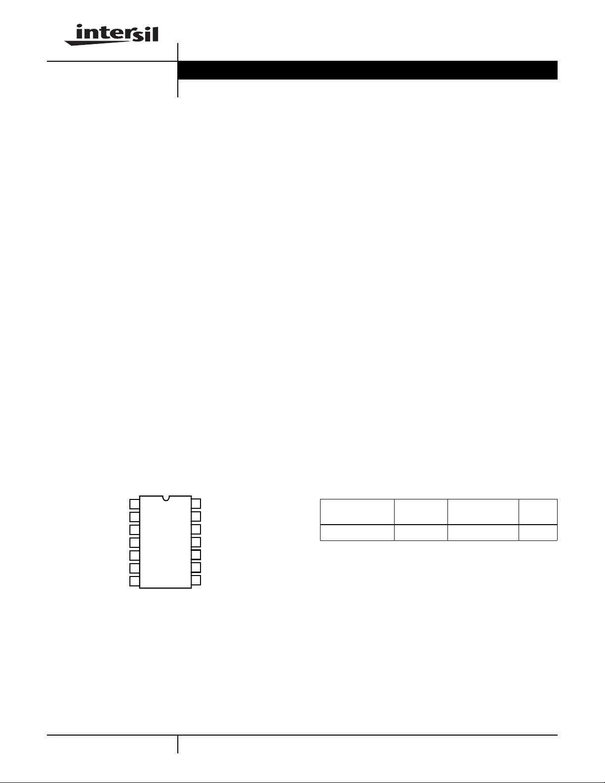
Pinout
HIP6012
(SOIC)
TOP VIEW
4324
Features
• Drives Two N-Channel MOSFETs
• Operates From +5V or +12V Input
• Simple Single-Loop Control Design
- Voltage-Mode PWM Control
• Fast Transient Response
- High-Bandwidth Error Amplifier
- Full 0% to 100% Duty Ratio
• Excellent Output Voltage Regulation
- 1.27V Internal Reference
- ±1.5% Over Line Voltage and Temperature
• Over-Current Fault Monitor
- Does Not Require Extra Current Sensing Element
- Uses MOSFETs r
DS(ON)
• Small Converter Size
- Constant Frequency Operation
- 200kHz Free-Running Oscillator Programmable from
50kHz to Over 1MHz
• 14 Pin, SOIC Package
Applications
• Power Supply for Pentium®, Pentium Pro, PowerPC™ and
Alpha™ Microprocessors
• High-Power 5V to 3.xV DC-DC Regulators
• Low-Voltage Distributed Power Supplies
RT
OCSET
SS
COMP
FB
EN
GND
1
2
3
4
5
6
7
2-152
14
13
12
11
10
9
8
VCC
PVCC
LGATE
PGND
BOOT
UGATE
PHASE
Ordering Information
TEMP.
PART NUMBER
HIP6012CB 0 to 70 14 Ld SOIC M14.15
CAUTION: These devices are sensitive to electrostatic discharge; follow proper IC Handling Procedures.
http://www.intersil.com or 407-727-9207
RANGE (oC) PACKAGE
PowerPC™ is a trademark of IBM.
Alpha™ is a trademark of Digital Equipment Corporation.
Pentium® is a registered trademark of Intel Corporation.
| Copyright © Intersil Corporation 1999
PKG.
NO.

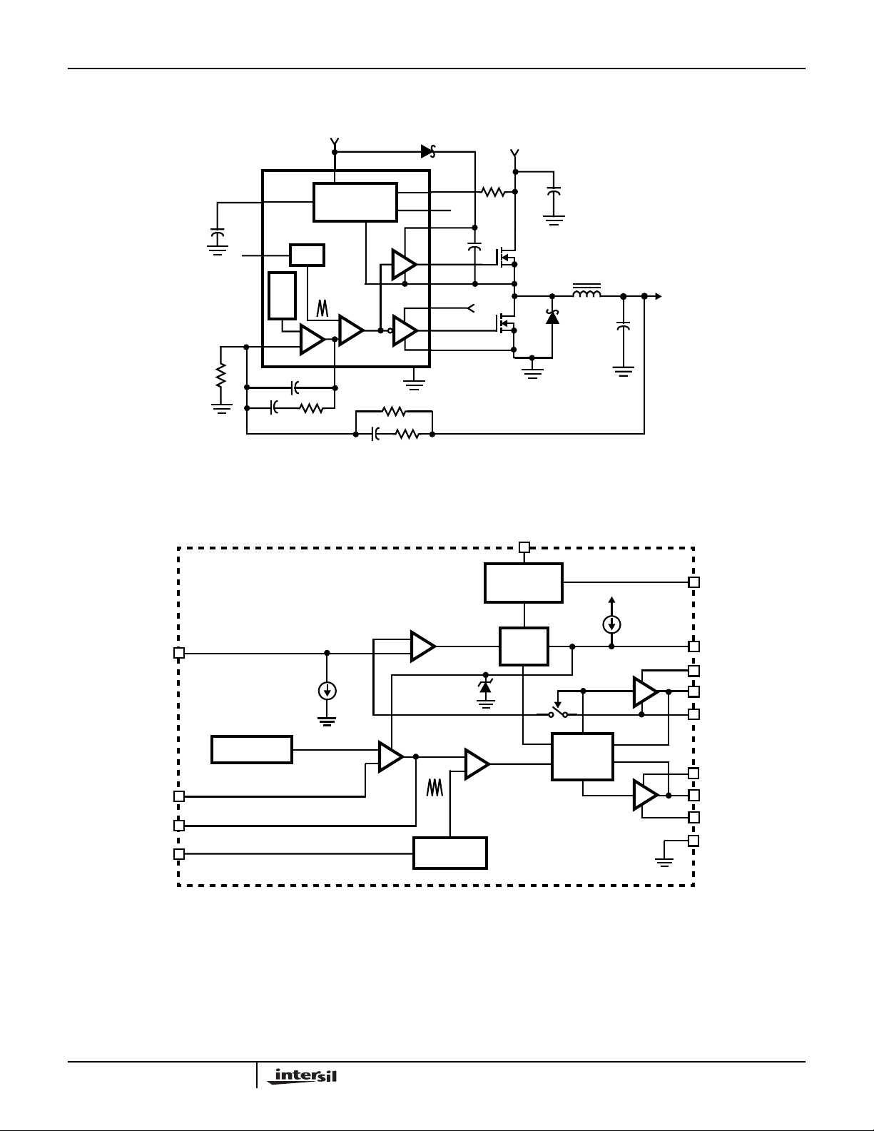
Typical Application
12V
VCC
HIP6012
+5V OR +12V
Block Diagram
SS
RT
FB
REF
MONITOR AND
PROTECTION
OSC
HIP6012
+
-
COMP
OCSET
EN
BOOT
UGATE
PHASE
+12V
PVCC
-
+
LGATE
PGND
GND
VCC
POWER-ON
RESET (POR)
+V
O
EN
OCSET
FB
COMP
RT
REFERENCE
200µA
1.27 VREF
+
-
ERROR
AMP
+
-
OVER-
CURRENT
4V
PWM
COMPARATOR
OSCILLATOR
10µA
SOFT-
START
+
-
INHIBIT
PWM
GATE
CONTROL
LOGIC
SS
BOOT
UGATE
PHASE
PVCC
LGATE
PGND
GND
2-153

HIP6012
Absolute Maximum Ratings Thermal Information
Supply Voltage, VCC . . . . . . . . . . . . . . . . . . . . . . . . . . . . . . . +15.0V
Boot Voltage, V
BOOT
- V
. . . . . . . . . . . . . . . . . . . . . . . +15.0V
PHASE
Input, Output or I/O Voltage. . . . . . . . . . . .GND -0.3V to VCC +0.3V
ESD Classification . . . . . . . . . . . . . . . . . . . . . . . . . . . . . . . . .Class 2
Operating Conditions
Supply Voltage, VCC . . . . . . . . . . . . . . . . . . . . . . . . . . . +12V ±10%
Ambient Temperature Range. . . . . . . . . . . . . . . . . . . . .0oC to 70oC
Junction Temperature Range. . . . . . . . . . . . . . . . . . . .0oC to 125oC
CAUTION: Stresses above those listed in “Absolute Maximum Ratings” may cause permanent damage to the device. This is a stress only rating and operationofthe
device at these or any other conditions above those indicated in the operational sections of this specification is not implied.
NOTE:
1. θJA is measured with the component mounted on an evaluation PC board in free air.
Electrical Specifications Recommended Operating Conditions, Unless Otherwise Noted
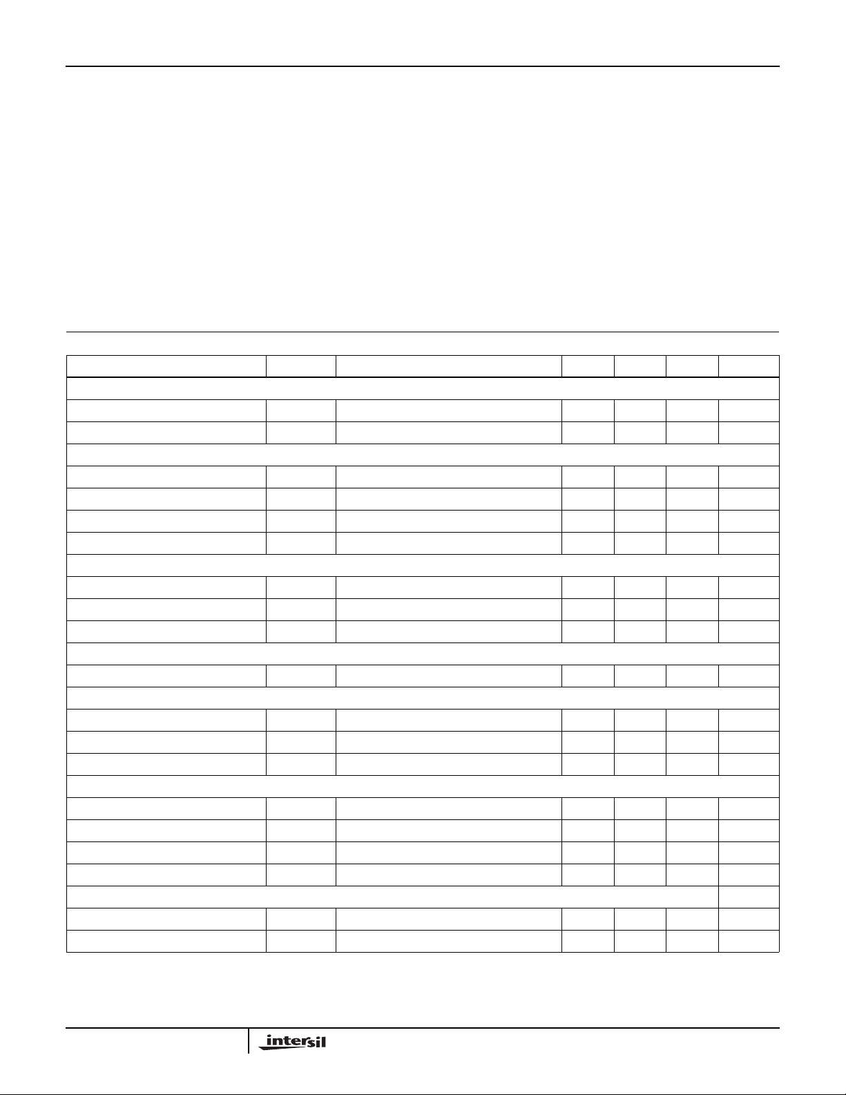
PARAMETER SYMBOL TEST CONDITIONS MIN TYP MAX UNITS
VCC SUPPLY CURRENT
Nominal Supply I
CC
Shutdown Supply EN = 0V - 50 100 µA
POWER-ON RESET
Rising VCC Threshold V
Falling VCC Threshold V
Enable - Input threshold Voltage V
Rising V
Threshold - 1.27 - V
OCSET
OSCILLATOR
Free Running Frequency RT = OPEN, VCC = 12 180 200 220 kHz
Total Variation 6kΩ < RT to GND < 200kΩ -20 - +20 %
Ramp Amplitude ∆V
OSC
REFERENCE
Reference Voltage 1.251 1.270 1.289 V
ERROR AMPLIFIER
DC Gain -88- dB
Gain-Bandwidth Product GBW - 15 - MHz
Slew Rate SR COMP = 10pF - 6 - V/µs
GATE DRIVERS
Upper Gate Source I
Upper Gate Sink R
Lower Gate Source I
Lower Gate Sink R
UGATE
UGATEILGATE
LGATE
LGATEILGATE
PROTECTION
OCSET Current Source I
Soft Start Current I
OCSETVOCSET
SS
EN = VCC; UGATE and LGATE Open - 5 - mA
= 4.5VDC - - 10.4 V
OCSET
= 4.5VDC 8.8 - - V
OCSET
= 4.5VDC 0.8 - 2.0 V
OCSET
RT = OPEN - 1.9 - V
V
- V
BOOT
PHASE
= 0.3A - 5.5 10 Ω
VCC = 12V, V
= 0.3A - 3.5 6.5 Ω
= 4.5VDC 170 200 230 µA
Thermal Resistance (Typical, Note 1) θJA (oC/W)
SOIC Package . . . . . . . . . . . . . . . . . . . . . . . . . . . . . 115
Maximum Junction Temperature . . . . . . . . . . . . . . . . . . . . . . 150oC
Maximum Storage Temperature Range. . . . . . . . . . -65oC to 150oC
Maximum Lead Temperature (Soldering 10s) . . . . . . . . . . . . 300oC
(Lead tips only)
= 12V, V
= 6V 300 450 - mA
LGATE
= 6V 350 500 - mA
UGATE
-10- µA
P-P
2-154
 Loading...