Intersil Corporation HIP6011 Datasheet

September 1997
HIP6011
Buck Pulse-Width Modulator (PWM) Controller
and Output Voltage Monitor
Features
• Drives N-Channel MOSFET
• Operates From +5V or +12V Input
• Simple Single-Loop Control Design
- Voltage-Mode PWM Control
• Fast Transient Response
- High-Bandwidth Error Amplifier
- Full 0% to 100% Duty Ratio
• Excellent Output Voltage Regulation
- 1.27V Internal Reference
- ±1.5% Over Line Voltage and Temperature
• Over-Voltage and Over-Current Fault Monitors
- Does Not Require Extra Current Sensing Element
- Uses MOSFET’s r
DS(ON)
• Small Converter Size
- Constant Frequency Operation
- 200kHz Free-Running Oscillator Programmable
from 50kHz to Over 1MHz
Applications
• Power Supply for Pentium™, Pentium-Pro™,
PowerPC™ and Alpha™ Microprocessors
• High-Power 5V to 3.xV DC-DC Regulators
• Low-Voltage Distributed Power Supplies
Description
The HIP6011 provides complete control and protection for a
DC-DC converter optimized for high-perfor mance microprocessor applications. It is designed to drive an N-Channel
MOSFET in a standard buck topology. The HIP6011 integrates all of the control, output adjustment, monitoring and
protection functions into a single package.
The output voltage of the converter can be precisely regulated to as low as 1.27V, with a maximum tolerance of ±1.5%
over temperature and line voltage variations.
The HIP6011 provides simple, single feedbac k loop, voltagemode control with fast transient response. It includes a
200kHz free-running triangle-wave oscillator that is adjustable from below 50kHz to over 1MHz. The error amplifier
features a 15MHz gain-bandwidth product and 6V/µs slew
rate which enables high converter bandwidth for fast transient performance. The resulting PWM duty ratio ranges
from 0% to 100%.
The HIP6011 protects against over-current conditions by inhibiting PWM operation. The HIP6011 monitors the current by
using the r
of the upper MOSFET which eliminates the
DS(ON)
need for a current sensing resistor. Built-in over-voltage protection triggers an external SCR to crowbar the input supply.
Ordering Information
TEMP.
PART NUMBER
HIP6011 0 to 70 14 Ld SOIC M14.15
RANGE (oC) PACKAGE
PKG.
NO.
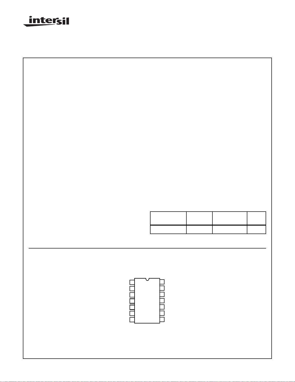
Pinout
HIP6011
(SOIC)
TOP VIEW
VSEN
1
OCSET
Alpha™ is a trademark of Digital Equipment Corporation.
Pentium™ is a trademark of Intel Corporation.
Pentium™ Pro is a trademark of Intel Corporation.
PowerPC™ is a trademark of IBM.
CAUTION: These devices are sensitive to electrostatic discharge; follow proper IC Handling Procedures.
www.intersil.com or 407-727-9207
| Copyright © Intersil Corporation 1999
SS
COMP
FB
EN
GND
2
3
4
5
6
7
14
RT
13
OVP
12
VCC
11
NC
10
BOOT
9
UGATE
8
PHASE
1
File Number 4409

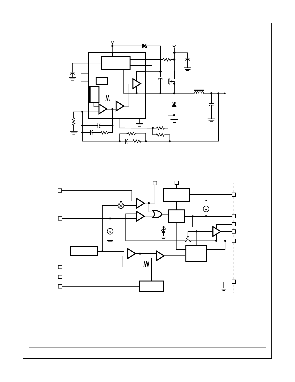
Typical Application
HIP6011
Block Diagram
SS
OVP
RT
FB
OSC
REF
+12V
VCC
MONITOR AND
PROTECTION
HIP6011
+
-
COMP
-
+
VSEN
GND
OCSET
EN
BOOT
UGATE
PHASE
OVP
+5V OR +12V
VCC
+V
O
VSEN
OCSET
FB
COMP
RT
REFERENCE
115%
200µA
1.27V REF
+
-
ERROR
AMP
OVER-
VOLTAGE
+
-
+
-
OVER-
CURRENT
COMPARATOR
OSCILLATOR
4V
PWM
+
-
POWER-ON
RESET (POR)
SOFT-
START
INHIBIT
PWM
GATE
CONTROL
LOGIC
EN
10µA
SS
BOOT
UGATE
PHASE
GND
All Intersil semiconductor products are manufactured, assembled and tested under ISO9000 quality systems certification.
Intersil products are sold by description only. Intersil Cor poration reserves the right to make changes in circuit design and/or specifications at any time without
notice. Accordingly, the reader is cautioned to verify that data sheets are current before placing orders. Information furnished by Intersil is believed to be accurate
and reliable. However, no responsibility is assumed by Intersil or its subsidiaries for its use; nor for any infringements of patents or other rights of third parties which
may result from its use. No license is granted by implication or otherwise under an y patent or patent rights of Intersil or its subsidiaries.
For information regarding Intersil Corporation and its products, see web site http://www.intersil.com
2

HIP6011
Absolute Maximum Ratings T
Supply Voltage, VCC. . . . . . . . . . . . . . . . . . . . . . . . . . . . . . . .+15.0V
Boot Voltage, V
BOOT
- V
. . . . . . . . . . . . . . . . . . . . . . .+15.0V
PHASE
Input, Output or I/O Voltage . . . . . . . . . . . . GND-0.3V to VCC+0.3V
ESD Classification . . . . . . . . . . . . . . . . . . . . . . . . . . . . . . . . Class 2
Recommended Operating Conditions
=25oC Thermal Information
A
Thermal Resistance (Typical, Note 1) θJA (oC/W)
SOIC Package. . . . . . . . . . . . . . . . . . . . . . . . . . . . . 150
Maximum Junction Temperature. . . . . . . . . . . . . . . . . . . . . . .150oC
Maximum Storage Temperature Range . . . . . . . . . .-65oC to 150oC
Maximum Lead Temperature (Soldering 10s). . . . . . . . . . . . .300oC
(SOIC - Lead Tips Only)
Supply Voltage, VCC . . . . . . . . . . . . . . . . . . . . . . . . . . . +12V ±10%
Ambient Temperature Range . . . . . . . . . . . . . . . . . . . . .0oC to 70oC
Junction Temperature Range . . . . . . . . . . . . . . . . . . . .0oC to 125oC
CAUTION: Stresses above those listed in “Absolute Maximum Ratings” may cause permanent damage to the device. This is a stress only rating and operation
of the device at these or any other conditions above those indicated in the operational sections of this specification is not implied.
NOTE:
1. θJA is measured with the component mounted on an evaluation PC board in free air.
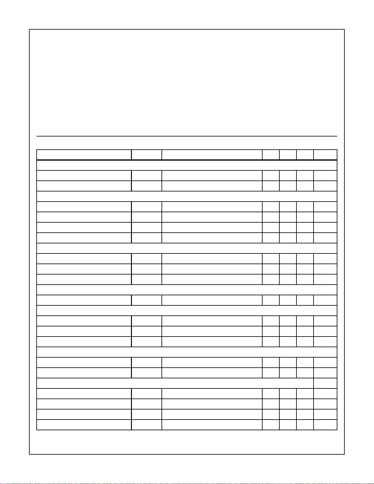
Electrical Specifications Recommended Operating Conditions, Unless Otherwise Noted
PARAMETER SYMBOL TEST CONDITIONS MIN TYP MAX UNITS
VCC SUPPLY CURRENT
Nominal Supply I
CC
Shutdown Supply EN = 0V 50 100 µA
POWER-ON RESET
Rising VCC Threshold V
Falling VCC Threshold V
Enable - Input threshold Voltage V
Rising V
Threshold 1.26 V
OCSET
OSCILLATOR
Free Running Frequency RT = OPEN, VCC = 12V 180 200 220 kHz
Total Variation 6kΩ < RT to GND < 200kΩ -20 +20 %
Ramp Amplitude ∆V
OSC
REFERENCE
Reference Voltage V
REF
ERROR AMPLIFIER
DC Gain 88 dB
Gain-Bandwidth Product GBW 15 MHz
Slew Rate SR COMP = 10pF 6 V/µs
GATE DRIVERS
Upper Gate Source I
Upper Gate Sink
UGATE
R
UGATE
PROTECTION
Over-Voltage Trip (V
SEN/VREF
OCSET Current Source I
OVP Sourcing Current I
Soft Start Current I
) 115 120 %
OCSETVOCSET
OVP
SS
EN = VCC; UGATE and LGATE open 5 mA
= 4.5VDC 10.4 V
OCSET
= 4.5VDC 8.2 V
OCSET
= 4.5VDC 0.8 2.0 V
OCSET
RT = OPEN 1.9 V
P-P
1.251 1.270 1.289 V
V
- V
BOOT
I
= 0.3A 5.5 10 Ω
LGATE
PHASE
= 12V, V
= 6V 350 500 mA
UGATE
= 4.5VDC 170 200 230 µA
V
SEN
= 5.5V; V
= 0V 60 mA
OVP
10 µA
3
 Loading...