Intersil Corporation HIP6004BCV, HIP6004BCB Datasheet

TM
HIP6004B
HIP6004B
Data Sheet February 1999 FN 4 567.2
Buck and Synchronous-Rectifier (PWM)
Controller and Output Voltage Monitor
The HIP6004B provides complete control and protection for
a DC-DC converter op timize d for high-p erformance
microprocessor applicatio ns. It is desi gned to dri ve two
N-Channel MOSF ETs i n a synchron ous- recti fied bu ck
topology. The HIP6004B integrates all of the control, output
adjustment, monitorin g and protect ion f uncti ons into a
single package.
The output voltage of the conver ter is eas ily adjusted and
precisely regulated. The H IP6004B in cludes a f ully TTLcompatible 5-input digital -to-a nalog converter (DAC) that
adjusts the output voltage from 1. 3V
0.05V and from 2.1V
to 3.5VDC in 0.1V increments
DC
to 2.05VDC in
DC
steps. The precision reference and voltage-mode regulator
hold the selected output voltage to w ithin ±1% over
temperature and line voltag e var iation s.
The HIP6004B provides si mp le, single f eedba ck loop,
voltage-mode cont rol with fast transie nt res ponse. I t
includes a 200kHz free-running triangle-wave oscillator that
is adjustable from below 50 kHz to over 1M Hz. The err or
amplifier features a 15MHz gain-bandwidth product and
6V/µs slew rate which enables high converter bandwidth for
fast transient performance . The re sulting P WM duty rat io
ranges from 0% to 100%.
The HIP6004B mon itors the out pu t voltage with a w indow
comparator that tracks the DAC output and issues a Power
Good signal when the outp ut is withi n ±10%. The
HIP6004B protec ts agai nst over -cur rent and over vo ltage
conditions by inhibiting PWM operat ion. Add itional bui lt-in
overvoltage protection triggers an external SCR to crowbar
the input supply. The HIP 6004B monitor s the cur rent by
using the r
of the upper MOSFET w hi ch elimin ates
DS(ON)
the need for a current sensing resistor .
Ordering Information
TEMP.
PART NUMBER
HIP6004BCB 0 to 70 20 Ld SOIC M20.3
HIP60 04 BC V 0 to 70 20 Ld TSS OP M20.17 3
NOTE: When ordering, use the entire part number. Add the suffix T
to obtain the TSSOP variant in tape and reel, e.g., HIP6004BCV-T.
RANGE (oC) PACKAGE
PKG.
NO.
Features
• Drives Two N-Channel MOSFETs
• Operates from +5V or +12V Input
• Simple Single-Loop Control Design
- Voltage-Mode PWM Cont rol
• Fast Transient Response
- High-Bandwidth Error Amplifier
- Full 0% to 1 00% D u ty Rat io
• Excellent Output Voltage Regulation
- ±1% Over Line Voltage and Temperature
• TTL-Compatible 5-Bit Digital-to-Analog Output
Voltage S e lect io n
- Wide Range . . . . . . . . . . . . . . . . . . . 1.3V
DC
to 3.5V
- 0.1V Binary Steps . . . . . . . . . . . . . . 2.1VDC to 3.5V
- 0.05V Bina ry S te p s . . . . . . . . . . . . 1.3VDC to 2.05V
• Power-Good Output Voltage M onitor
• Over-Voltage and Over -Current Fault Monitors
- Does Not Require Extra Current Sensing Element,
Uses MOSFET’s r
DS(ON)
• Small Converter Size
- Constant Fr equency Operation
- 200kHz Free-Ru nning Oscillator Programmable from
50kHz to over 1MHz
Applications
• Power Supply for Pentium®, Pentium Pro, Pentium II,
PowerPC™, K6™, 6X86™ and Alpha™ Microprocessors
•
High-Power 5V to 3.xV DC-DC Regulators
•
Low-Voltage Distributed Power Supplies
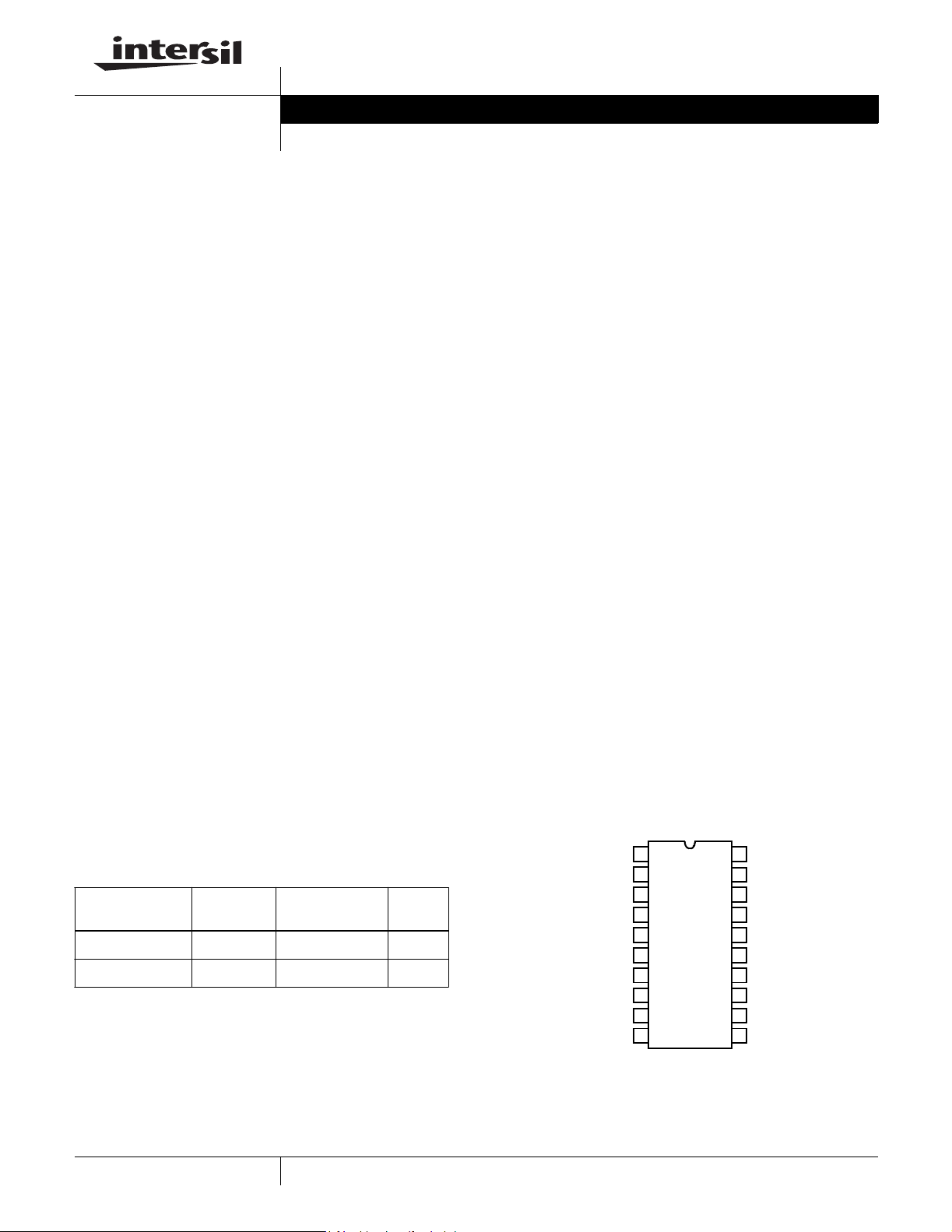
Pinout
HIP6004B
(SOIC, TSSOP)
TOP VIEW
VSEN
OCSET
SS
VID0
VID1
VID2
VID3
VID4
COMP
FB
1
2
3
4
5
6
7
8
9
10
20
19
18
17
16
15
14
13
12
11
RT
OVP
VCC
LGATE
PGND
BOOT
UGATE
PHASE
PGOOD
GND
DC
DC
DC
74
6X86™ is a trademark of Cyrix Corporation.
Alpha™ is a trademark of Digital Equipment Corporation.
K6™ is a trademark of Advanced Micro Devices, Inc.
Pentium® is a registered trademark of Intel Corporation.
PowerPC™ is a trademark of IBM.
CAUTION: These devices are sensitive to electrostatic discharge; follow proper IC Handling Procedures.
1-888-INTERSIL or 321-724-7143
| Intersil (and design) is a trademark of Intersil Americas Inc.
Copyright © Intersil Americas Inc. 2002. All Rights Reserved

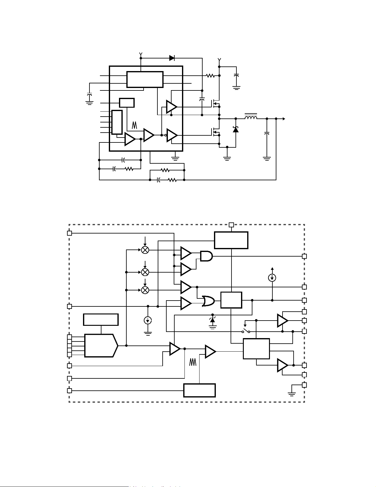
Typical Application
HIP6004B
Block Diagram
VSEN
OCSET
VID0
VID1
VID2
VID3
VID4
FB
COMP
RT
PGOOD
SS
OVP
RT
VID0
VID1
VID2
VID3
VID4
FB
REFERENCE
TTL D/A
CONVERTER
(DAC)
OSC
D/A
+12V
VCC
MONITOR AND
PROTECTION
HIP6004B
-
+
+
-
COMP
110%
90%
115%
200µA
DACOUT
VSEN
+
-
ERROR
AMP
OCSET
EN
BOOT
UGATE
PHASE
LGATE
PGND
GND
+
-
+
-
OVER-
VOLTAGE
+
-
+
-
OVER-
CURRENT
COMPARATOR
OSCILLATOR
4V
PWM
+
-
VIN = +5V OR +12V
VCC
POWER-ON
RESET (POR)
SOFT-
START
INHIBIT
PWM
GATE
CONTROL
LOGIC
+V
OUT
10µA
PGOOD
OVP
SS
BOOT
UGATE
PHASE
LGATE
PGND
GND

HIP6004B
Absolute Maximum Ratings Thermal Information
Supply Voltage, VCC . . . . . . . . . . . . . . . . . . . . . . . . . . . . . . . . .+15V
Boot Voltage, V
Input, Output or I/O Voltage. . . . . . . . . . . .GND -0.3V to V
ESD Classification . . . . . . . . . . . . . . . . . . . . . . . . . . . . . . . . .Class 2
BOOT
- V
. . . . . . . . . . . . . . . . . . . . . . . .+15V
PHASE
CC
+0.3V
Operating C o ndi t io ns
Supply Voltage, VCC . . . . . . . . . . . . . . . . . . . . . . . . . . . +12V ±10%
Ambient Temperature Range. . . . . . . . . . . . . . . . . . . . . 0
CAUTION: Stress es abov e thos e lis ted in “ A bsolute Max imum R a tings” ma y cause per manen t dam age to th e de vice. This is a s tress on ly rating and ope rat ion of th e
device at these or any other conditions above those indicated in the operational sections of this specification is not implied.
NOTE:
is measured with the compon ent mounted on an evaluation PC board in free air.
1. θ
JA
o
C to 70oC
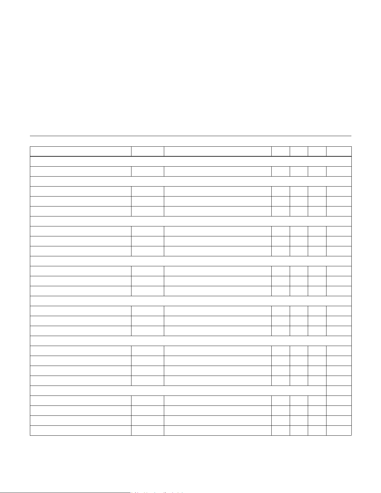
Electrical Specifications Recommended Op erating Conditions, Unless Otherwise Noted
PARAMETER SYMBOL TEST CONDITIONS MIN TYP MAX UNITS
V
SUPPLY CURRENT
CC
Nominal Supply I
CC
POWER-ON RESET
Rising V
Fallin g V
Rising V
Threshold V
CC
Threshold V
CC
Threshold -1.26- V
OCSET
OSCILLATOR
Free Running Frequency RT = OPEN 185 200 215 kHz
Total Vari ation 6kΩ < RT to GND < 200kΩ -15 - +15 %
Ramp Amplitude ∆V
OSC
REFERENCE AND DAC
DAC (VID0-VID4) Input Low Voltage --0.8V
DAC (VID0-VID4) Input High Voltage 2.0 - - V
DACOUT Voltage Accuracy -1.0 - +1.0 %
ERROR AMPLIFIER
DC Gain -88- dB
Gain- Ban dwidth Pr od uc t G B W - 15 - M H z
Slew Rate SR COMP = 10pF - 6 - V/µs
GATE DRIVERS
Upper Gate Source I
Upper Gate Sink R
Lower Gat e Source I
Lower Gate Sink R
UGATE
UGATEILGATE
LGATE
LGATEILGATE
PROTECTION
Over-Voltage Trip (V
OCSET Current Source I
OVP Sourcing Current I
Soft Start Current I
/DACOUT) -115120 %
SEN
OCSET
OVP
SS
UGATE and LGATE Open - 5 - mA
OCSET
OCSET
RT = Open - 1.9 - V
V
- V
BOOT
= 0.3A - 5.5 10 Ω
VCC = 12V, V
= 0.3A - 3.5 6.5 Ω
V
OCSET
V
= 5.5V, V
SEN
Thermal Resistance (Typical, Note 1)
SOIC Package . . . . . . . . . . . . . . . . . . . . . . . . . . . . . 110
SOIC Package (with 3in
2
of Copper). . . . . . . . . . . . 86
θ
JA
(oC/W)
TSSOP Package . . . . . . . . . . . . . . . . . . . . . . . . . . . 140
Maximum Junction Temperature . . . . . . . . . . . . . . . . . . . . . . 150
Maximum Storage Temperature Range . . . . . . . . . -65
o
C to 150oC
Maximum Lead Temperature (Soldering 10s). . . . . . . . . . . . 300
(Lead Tip s Onl y)
= 4.5V - - 10.4 V
= 4.5V 8.2 - - V
PHASE
= 4.5V
= 12V, V
= 6V 300 450 - mA
LGATE
DC
= 0V 60 - - mA
OVP
= 6V 350 500 - mA
UGATE
170 200 230 µA
-10- µA
P-P
o
C
o
C

HIP6004B
Electrical Specifications Recommended Op erating Conditions, Unless Otherwise Noted (Continued)
PARAMETER SYMBOL TEST CONDITIONS MIN TYP MAX UNITS
POWER GOOD
Upper Threshold (V
Lower Threshold (V
Hysteresis (V
SEN
PGOOD Voltage Low V
/DACOUT) V
SEN
/DACOUT) V
SEN
Rising 106 - 111 %
SEN
Falling 89 - 94 %
SEN
/ D AC OU T) Upper and Lower T h res hold - 2 - %
PGOODIPGOOD
= -5mA - 0.5 - V
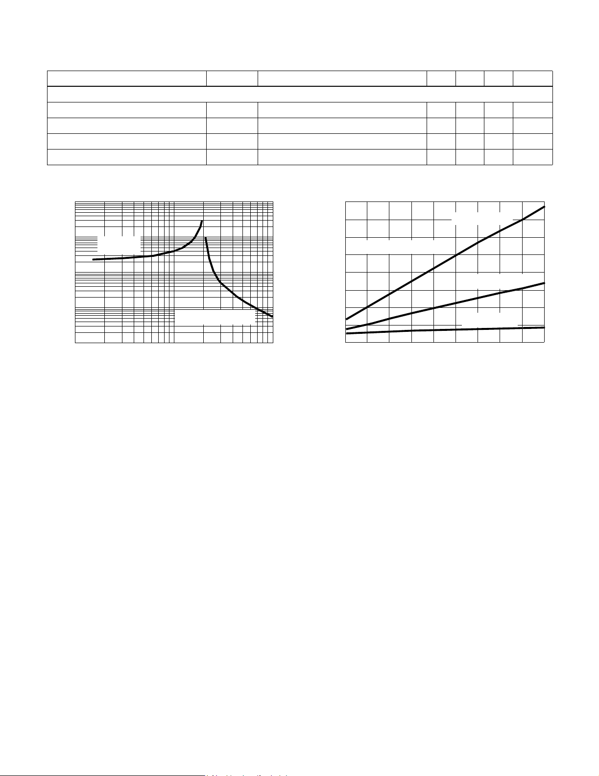
Typical Performance Curves
80
70
C
GATE
= 3300pF
1000
RESISTANCE (kΩ)
100
10
RT PULLUP
TO +12V
RT PULLDOWN TO V
10 100 1000
SWITCHING FREQUENCY (kHz)
SS
60
C
= C
UPPER
50
40
(mA)
CC
I
30
20
10
0
100 200 300 400 500 600 700 800 900 1000
= C
LOWER
SWITCHING FREQUENCY (kHz)
GATE
C
C
GATE
GATE
FIGURE 1. RT RESISTANCE vs FREQUENCY FIGURE 2. BIAS SUPPLY CURRENT vs FREQUENCY
= 1000pF
= 10pF
 Loading...