Intersil Corporation HIP5020 Datasheet
HIP5020
Data Sheet January 1997
Integrated-Power Buck Converter
Controller with Synchronous Rectification
The HIP5020 is a high-efficiency, buck converter controller
with synchronous rectification and integralpowerMOSFETs.
Integrated current sensing eliminates the external resistor
and saves power. The controller combines two methods of
regulation: Current mode control for outstanding regulation
response to large signal load transients, and Hysteretic
mode control for high efficiency at low output currents.
The HIP5020 controller offers a high degree of flexibility.
Small components set the switching frequency, the soft-start
interval and the load current boundary between Run and
Hysteretic modes. These adjustments enable the designer
to best optimize the trade-offs of cost, efficiency and size.
The example application guide section illustrates these
trade-offs with component and vendor suggestions for three
circuit designs. These designs are suitable for use without
modification. However, the block diagram, detailed
description and HIP5020 component specifications enable
further optimization to meet specific requirements.
File Number
Features
• High Efficiency - Above 95%
• Integrated N-Channel Synchronous Rectifier
and Upper MOSFETs - 75mΩ Each
• Wide Input Voltage and Load Range
- 4.5VDC to 18VDC (5 to 12 NiCd Battery Cells)
- Up to 3.5ADC
• Automatically Switches Regulation Mode
- Current Mode Control for Excellent Performance at
High Load Currents
- Hysteretic Control for High Efficiency at Light Load
Currents
• Flexible and Easy to Use
- Ready-to-Use Example Applications
- Custom Optimization with Small Components
- Design and Simulation Software Available
• Integrated, Low-Loss Current Sensing
• Over-Current Protection
4243
Ordering Information
TEMP.
PART NUMBER
RANGE (oC) PACKAGE
HIP5020DB 0 to 70 28 Ld SOIC M28.3
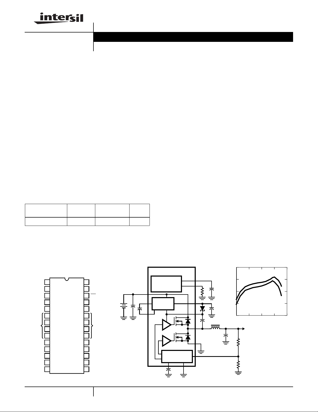
Pinout
Typical Application
HIP5020 (SOIC)
TOP VIEW
28
27
26
25
24
23
22
21
20
19
18
17
16
15
PHASE
PHASE
SD
SOFT
OVLD
PGND
(WEB)
CPCP+
VCC
BOOT
CT
PHASE
PHASE
PGND
(WEB)
GND
VINF
HMI
SLOPE
VIN
VIN
VIN
FB
1
2
3
4
5
6
7
8
9
10
11
12
13
14
PKG.
NO.
V
IN
• Adaptive Dead-Time - Eliminates Shoot-Through
• 100kHz to 1MHz PWM Switching Frequency
• Thermally Enhanced SOIC Package
Applications
• Notebook Computers
• Portable Telecommunications
• Portable Instruments
HIP5020
MODE
CONTROL AND
PROTECTION
INTERNAL
SUPPLY
L1
14µH
440µF
REGULATION
AND CONTROL
100
95
90
85
EFFICIENCY (%)
80
0.001 0.01 0.1 1 10
C1
VIN = 6V
V
= 5V
O
V
= 5V
IN
VO = 3.3V
LOAD CURRENT (A)
V
OUT
2-13
CAUTION: These devices are sensitive to electrostatic discharge; follow proper IC Handling Procedures.
http://www.intersil.com or 407-727-9207
| Copyright © Intersil Corporation 1999
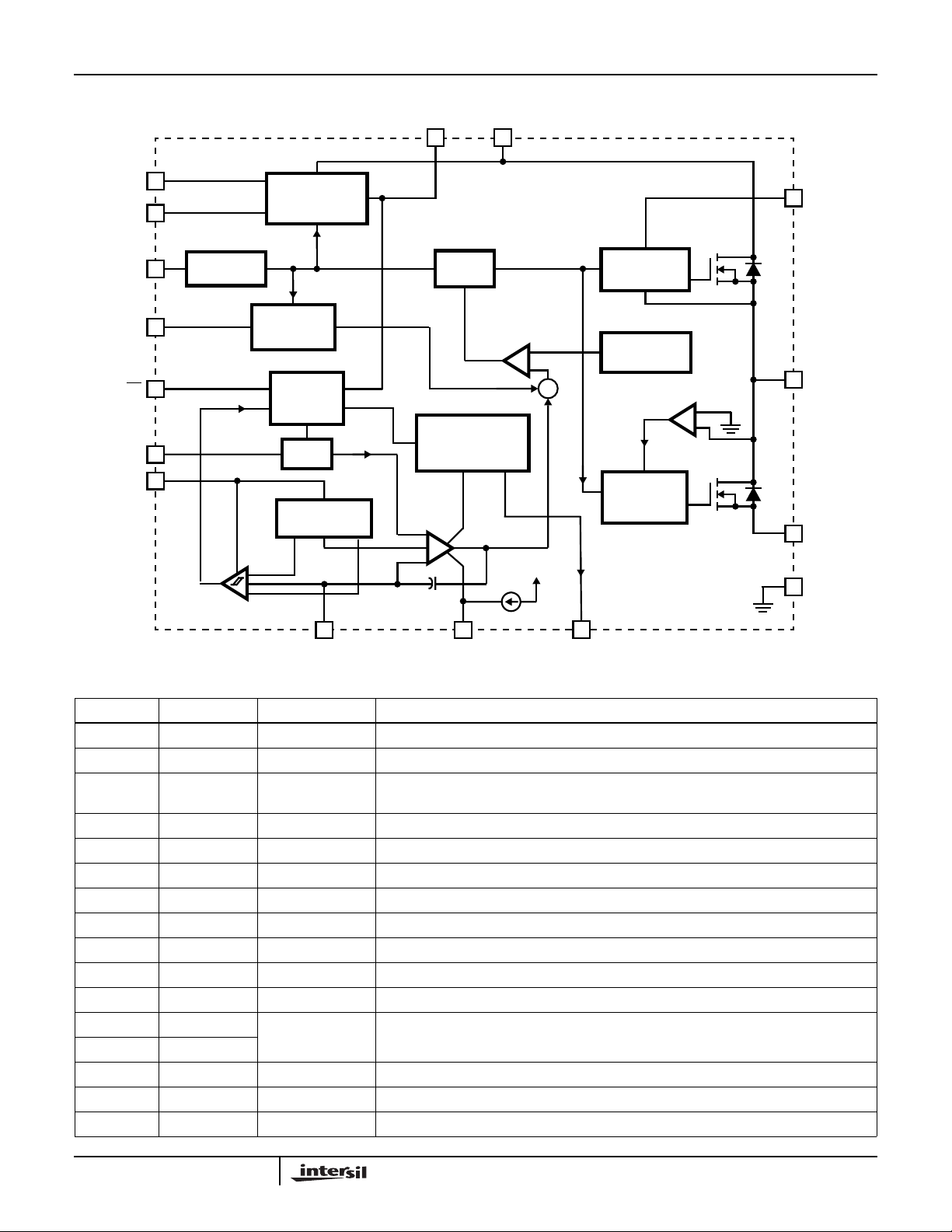
Functional Block Diagram
HIP5020
VINVCC
CP+
CP-
CT
SLOPE
SD
SOFT
VINF
OSCILLATOR
RUN
HYSTERETIC
CHARGE PUMP
REGULATOR
SLOPE
GENERATOR
MODE
CONTROL
LOGIC
SOFT-
START
REFERENCE
+
-
1.26V+∆ -∆
S
PWM
LATCH
R
OVER-CURRENT
PROTECTION
ERROR
AMP
+
+
-
12pF
PWM
20µA
BOOT
PWM
+
-
∑
-
+
V
CC
UPPER GATE
DRIVE
CURRENT
SENSOR
PHASE
LOWER GATE
DRIVE AND
LOGIC
PHASE
+
-
PGND
GND
FB
HMI
OVLD
Pin Description
PIN NO DESIGNATOR FUNCTION DESCRIPTION
1, 2, 3 VIN Input Voltage Connection to the power source (Battery). Operates from 4.5VDC to 18VDC.
4, 5, 27, 28 PHASE Switch Node Connect to output Inductor.
6, 7, 8,9,20,
21, 22, 23
10 GND Signal Ground Connect to the output load return.
11 FB Voltage Sense A divider network scales the output voltage to 1.26VDC.
12 VINF Filtered Input Connect a low-pass (R-C) filter from VIN.
13 HMI Hysteretic Current A resistor to the HMI pin sets the peak inductor current level during hysteretic mode.
14 SLOPE Ramp Set A capacitor to ground sets the compensation ramp for current mode control.
15 CT Frequency Set A capacitor to ground sets the oscillator frequency.
16 BOOT Bootstrap Bias A capacitor to Phase pin stores energy for the upper MOSFET drive.
17 VCC Bias Voltage Output of charge pump regulator. Use bypass capacitor to ground.
18 CP+ Charge Pump
19 CP24 OVLD Over-Load A high level on this pin signals activation of the current limit protection.
25 SOFT Soft Start A capacitor to ground sets the soft start interval.
26 SD Shutdown A low level suspends operation for a low-dissipation shutdown mode.
PGND Power Ground Power Return and thermal interface. Solder these pins to a large copper ground plane.
Connect a capacitor between these pins for the charge pump to generate bias power. The
Capacitor
internal charge pump inverter is synchronized to the oscillator.
2-14
HIP5020
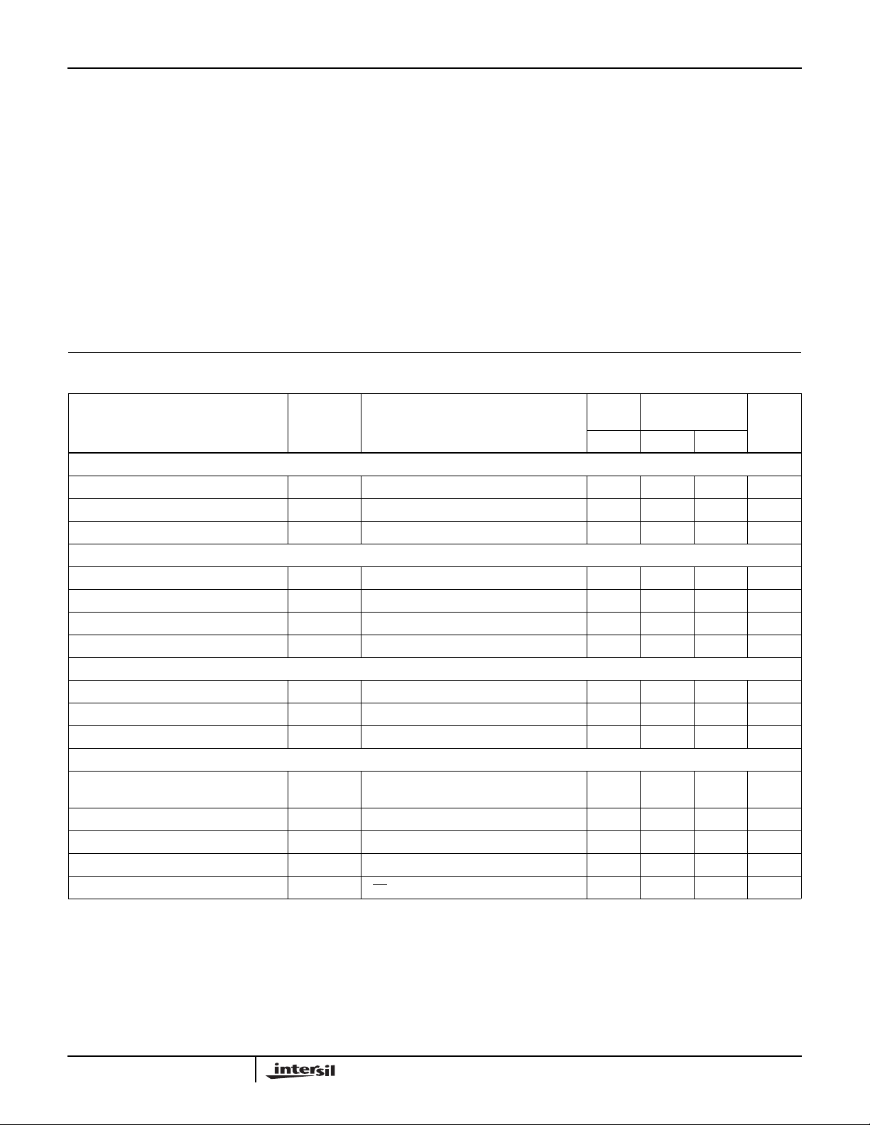
Absolute Maximum Ratings Thermal Information
Input Voltage, VIN . . . . . . . . . . . . . . . . . . . . . . . . . . -0.3V to +20.0V
Supply Voltage, VCC . . . . . . . . . . . . . . . . . . . . . . . . -0.3V to +20.0V
Shutdown Voltage . . . . . . . . . . . . . . . . . . . . . . . .-0.3V to VCC+0.3V
Voltage on PGND. . . . . . . . . . . . . . . . . . . . . . -2V to +2V (Transient)
All voltages are relative to GND, unless otherwise specified.
Operating Conditions
Voltage Range, VIN . . . . . . . . . . . . . . . . . . . . . . . . .+4.5V to +18.0V
Temperature Range . . . . . . . . . . . . . . . . . . . . . . . . . . . .0oC to 70oC
Oscillator Frequency Range. . . . . . . . . . . . . . . . . . 100kHz to 1MHz
CAUTION: Stresses above those listed in “Absolute Maximum Ratings” may cause permanent damage to the device. This is a stress only rating and operationofthe
device at these or any other conditions above those indicated in the operational sections of this specification is not implied.
NOTE:
1. θJA is measured with the component mounted on an evaluation PC board in free air.
Thermal Resistance (Typical, Note 1) θJA (oC/W)
Plastic SOIC Package . . . . . . . . . . . . . . . . . . . . . . . 51
Plastic SOIC Package (with 1in2 copper). . . . . . . . . 42
Plastic SOIC Package (with 3in2 copper). . . . . . . . . 39
Maximum Junction Temperature (Plastic Package) . . . . . . . .125oC
Maximum Storage Temperature Range. . . . . . . . . . -65oC to 150oC
Maximum Lead Temperature (Soldering 10s) . . . . . . . . . . . . .300oC
(SOIC - Lead Tips Only)
Electrical Specifications V
= 6.3VDC, Componentsreferencedfrom Figure 1. TYP values at TJ=25oC and MIN, MAX limits are forT
IN
from 0oC to 125oC; Unless Otherwise Specified
T
=
J
25oC0oC < TJ < 125oC
PARAMETER SYMBOL TEST CONDITIONS
UNITSTYP MIN MAX
REFERENCE
Reference Voltage V
FB
Total Variation, IO > I
HMI
1.26 1.235 1.285 V
Temperature Stability - - 0.2 mV
Hysteresis Width 2∆ Hysteresis Mode; IO < I
HMI
20 10 30 mV
MODE CONTROL LOGIC
Under-Voltage Lockout Threshold VCC
Under-Voltage Lockout Hysteresis ∆VCC
Shutdown Threshold V
HMI Current Source I
SD
HMI
UV
UV
7.6 7.2 7.9 V
0.3 - - V
1.2 0.9 1.5 V
20 16 29 µA
POWER MOSFETs
Drain Leakage Current I
On State Resistance r
DSS
DS(ON)VBOOT
Phase Rise and Fall Time tr, t
V
= 20V, V
DSS
- V
PHASE
IO = 2ADC 10 - - ns
f
= 0 0.35 - 10 µA
PHASE
= 12.6V; I
= 2A 75 60 125 mΩ
PHASE
CHARGE PUMP REGULATOR
VCC Regulation V
CC
VIN = 8.65V; FS = 100kHz;
14.8 14.0 16.0 V
C4 = C5 = 1.0µF
Charge Pump Disable V
VCC Current - Run Mode I
INCPN
CC
FS = 100kHz 4 - - mA
9.8 - - V
VINF Current - Hysteretic Mode ICC - Idle VFB = 5V, VCT = 0 78 - 110 µA
VCC Current - Shutdown I
CC
VSD = GND, VIN = 12V 2 - 17 µA
J
2-15
HIP5020
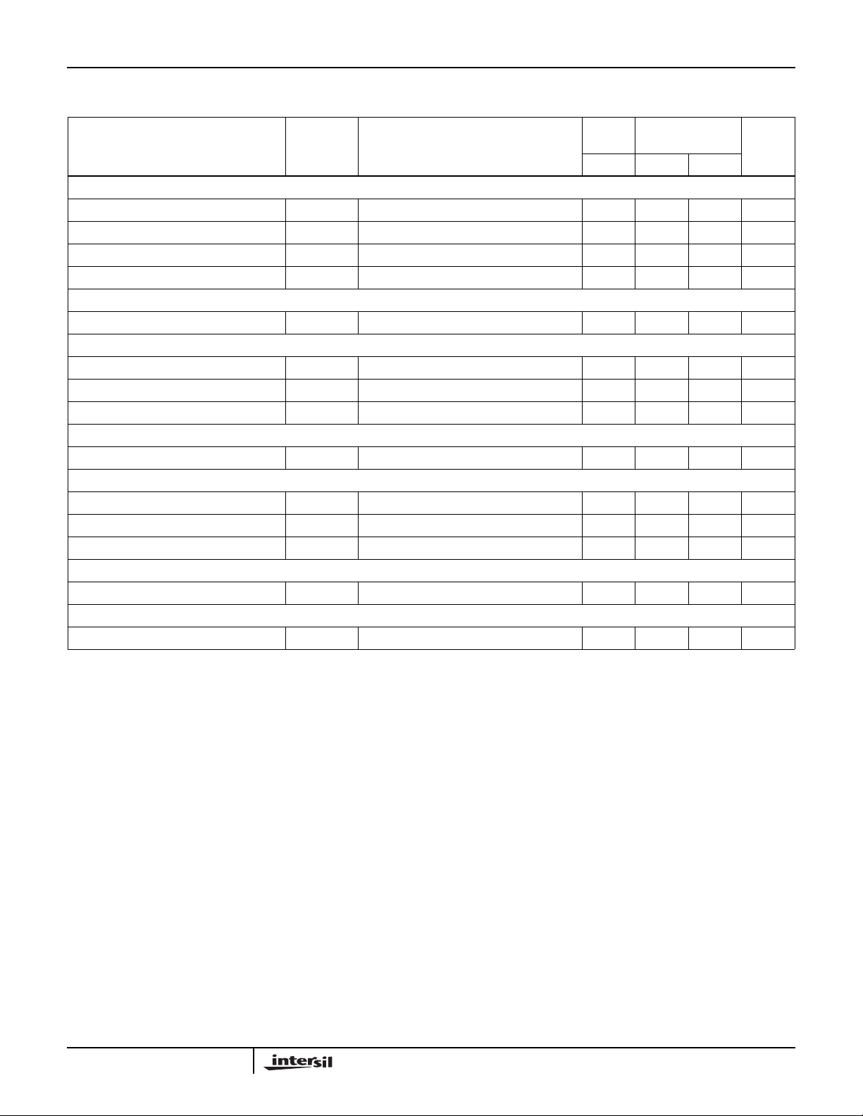
Electrical Specifications V
PARAMETER SYMBOL TEST CONDITIONS
ERROR AMPLIFIER
Internal Integration Capacitor 12 - - pF
Open-Loop Voltage Gain AV 89 - - dB
Gain-Bandwidth Product GBW 7.2 - - MHz
Input Bias Current I
SOFT START
Current Source I
OSCILLATOR
CT Charging Current 126 110 140 µA
Initial Frequency Accuracy ±3- -%
Total Frequency Variation VIN = 4.5 to 18V ±7-±10 %
PROTECTIVE FUNCTION
Current Limit Threshold I
PWM MODULATOR
Modulator Gain 1.7 - - A/V
Minimum On Time 100 - - ns
Minimum Off Time 115 - - ns
HYSTERETIC COMPARATOR
Propagation Delay Step V
SLOPE GENERATOR
Slope Capacitor Charge Current I
= 6.3VDC, Componentsreferencedfrom Figure 1. TYP values at TJ=25oC and MIN, MAX limits are forT
IN
from 0oC to 125oC; Unless Otherwise Specified (Continued)
=
T
J
25oC0oC < TJ < 125oC
FB
SOFT
O PK
SLOPE
VFB = 1.26VDC 3 -70 70 nA
10 6 14 µA
4.5 4 - A
FB
3--µs
80 - - µA
J
UNITSTYP MIN MAX
Example Application Guide
The HIP5020 provides the flexibility to meet differing needs.
This section illustrates the trade-off of component selection
for three DC-DC converter circuit designs. Each circuit is
optimized for a specific goal: Circuit 1 is optimized for high
efficiency, Circuit 2 is optimized for small size, and Circuit 3
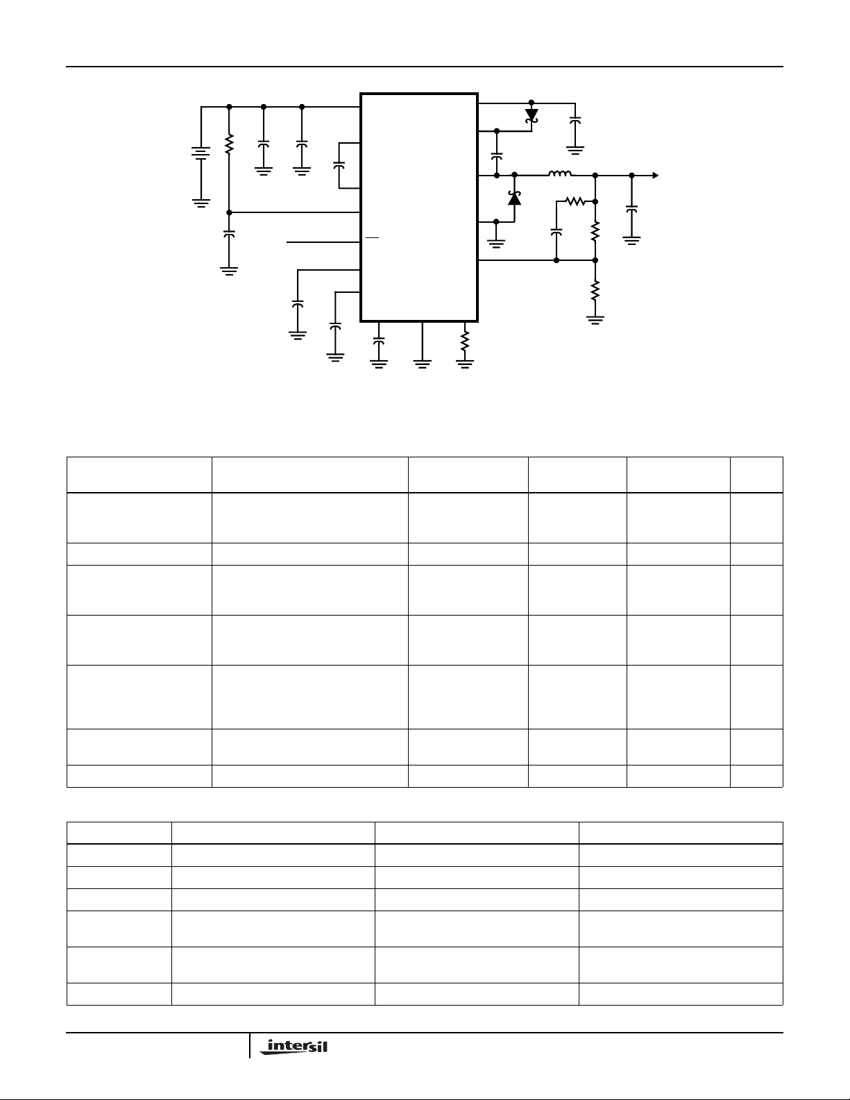
is optimized for low cost. Figure 1 shows the schematic
common to all three converter designs. Table 1 shows the
expected performance parameters for each circuit. Table 2
gives the value of each component referenced in Figure 1.
Table 3 provides a listing of suggested vendors for the major
(or critical) components. Figures 2, 3 and 4 show the
efficiency and transient performance of each circuit.
2-16
HIP5020
VIN
+
V
IN
-
R5
C10
C2
C12
C5
ON/OFF
C6
CP+
HIP5020
CP-
VINF
SD
CT
SLOPE
SOFT GND
C7
C8
VCC
BOOT
PHASE
PGND
FB
OVLD
HMI
R4
C3
D2
D1
L1
C9
R6
C4
R1
R2
C1
V
O
FIGURE 1. EXAMPLE APPLICATION CIRCUIT
TABLE 1. EXAMPLE APPLICATION PERFORMANCE PARAMETERS
These characteristics are for the circuit shown in Figure 1 with the components given in Tables 2 and 3.
PARAMETER CONDITIONS
Input Voltage
- Typical
- Range
CIRCUIT 1
HIGH EFFICIENCY
3 Li-Ion Cells:
11.1
8.1 to 16
CIRCUIT 2
SMALL SIZE
2 Li-Ion Cells:
7.4
5.4 to 12
CIRCUIT 3
LOW COST UNITS
9 Nicd Cells:
10.8
VDC
8.1 to 16
Switching Frequency 200 ±15% 625 ±15% 120 ±20% kHz
Output Voltage Variation
Line Regulation
Load Regulation
Output Voltage Ripple
- Full Load
- Light Load
Initial Setting
Input Voltage Range; IO = 1ADC
IO = 0.1 to 3ADC, VIN = Typical
Bandwidth < 20MHz
IO = 3ADC, VIN = Typical
IO = 50mADC, VIN = Typical
3.3 ±3.5%
±0.1
±0.3
18
50
3.3 ±2.2%
±0.1
±0.3
30
80
3.3 ±3.5%
±0.1
±0.4
20
70
V
%
%
mV
Efficiency
- Full load
- Peak
- Light Load
Estimated Circuit Area
Tallest Component
IO = 3ADC, VIN = Typical
0.5 < IO < 2ADC, VIN = Typical
IO = 50mADC, VIN = Typical
86
92
88
3.5
0.45
86
89
84
2.1
0.24
86
90
72
3.6
0.68
%
%
%
in
in
Normalized Circuit Cost Ratio of total circuit cost to Circuit 2 1.1 1 0.75
2
TABLE 2. COMPONENT SUGGESTIONS FOR EXAMPLE APPLICATION CIRCUITS
COMPONENT CIRCUIT 1 CIRCUIT 2 CIRCUIT 3
D1 MBR0540 MBR0540 1N4148
D2 MBR0540 Not Used Not Used
L1 16µH, RDC < 15mΩ 5µH, RDC < 22mΩ 26µH, RDC < 25mΩ
C1 2x - 220µF, 10V OS-CON
ESR
(100kHz) < 35mΩ
MAX
C2 100µF, 20V OS-CON
ESR
(100kHz) < 30mΩ
MAX
3x - 220µF, 10V Tantalum
ESR
(100kHz) < 100mΩ
MAX
2x - 100µF, 16V Tantalum
ESR
(100kHz) < 100mΩ
MAX
3x - 390µF, 25V, Aluminum
ESR
(100kHz) < 65mΩ
MAX
2x - 390µF, 25V Aluminum
ESR
(100kHz) < 65mΩ
MAX
C3 0.1µF ±20% - Ceramic 0.1µF ±10% - Ceramic 0.1µF ±20% - Ceramic
2-17
 Loading...