HIP4086
Data Sheet May 1999
80V, 0.5A Three Phase Driver
The HIP4086 is a Three Phase Bridge N-Channel MOSFET
driver IC. The HIP4086 is specifically targeted for PWM
motor control. It makes bridge based designs simple and
flexible. Like the HIP4081, the HIP4086 has a flexible input
protocol for drivingeverypossible switch combination. Unlike
the HIP4081, the user can override the shoot-through
protection for switched reluctance applications. TheHIP4086
has reduced drive current compared to the HIP4081 (0.5A
vs 2.5A) and a much wider range of programmable dead
times (0.25µs to 4.5µs) - like the HIP4082. The HIP4086 is
suitable for applications requiring DC to 100kHz. Unlike the
previous family members, the HIP4086 has a programmable
undervoltage set point.
Also refer to the HIP4083, three phase upper only MOSFET
driver, for a lower current solution optimized for smaller
motors.
Ordering Information
PART NUMBER
TEMP.
RANGE (oC) PACKAGE
PKG.
NO.
File Number
4220.4
Features
• Independently Drives 6 N-Channel MOSFETs in Three
Phase Bridge Configuration
• Bootstrap Supply Max Voltage to 95VDC
• Bias Supply Operation from 7V to 15V
• 1.25A Peak Turn-Off Current
• User-Programmable Dead Time (0.25µs to 4.5µs)
• Charge-Pump and Bootstrap Maintain Upper Bias
Supplies
• Programmable Bootstrap Refresh Time
• Drives 1000pF Load with Typical Rise Time of 20ns and
Fall Time of 10ns
• DIS (Disable) Overrides Input Control
• Input Logic Thresholds Compatible with 5V to 15V Logic
Levels
• Dead Time Disable Capability
• Programmable Undervoltage Set Point
HIP4086AB -40 to 125 24 Ld SOIC M24.3
HIP4086AP -40 to 125 24 Ld PDIP E24.3
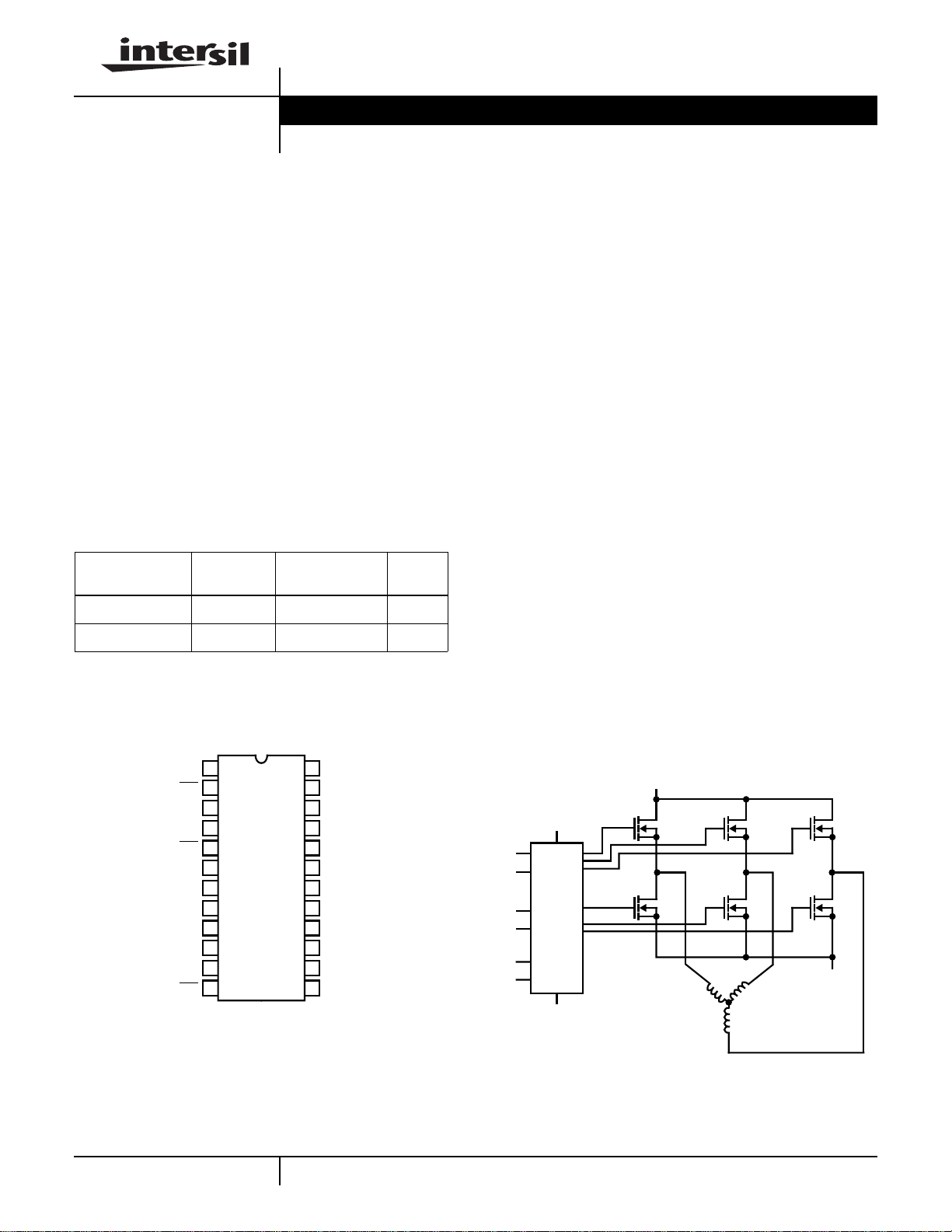
Pinout
HIP4086
(PDIP, SOIC)
TOP VIEW
BHB
BHI
BLI
ALI
AHI
V
SS
RDEL
UVLO
RFSH
DIS
CLI
CHI
1
2
3
4
5
6
7
8
9
10
11
12
BHO
24
BHS
23
BLO
22
ALO
21
V
20
DD
19
CLO
18
AHS
17
AHO
16
AHB
15
CHS
14
CHO
13
CHB
Applications
• Brushless Motors
• AC Motor Drives
• Switched Reluctance Motor Drives
• Battery Powered Vehicles
Application Block Diagram
80V
12V
HIP4086
GND
GND
1
CAUTION: These devices are sensitive to electrostatic discharge; follow proper IC Handling Procedures.
http://www.intersil.com or 407-727-9207
| Copyright © Intersil Corporation 1999

HIP4086
HIP4086
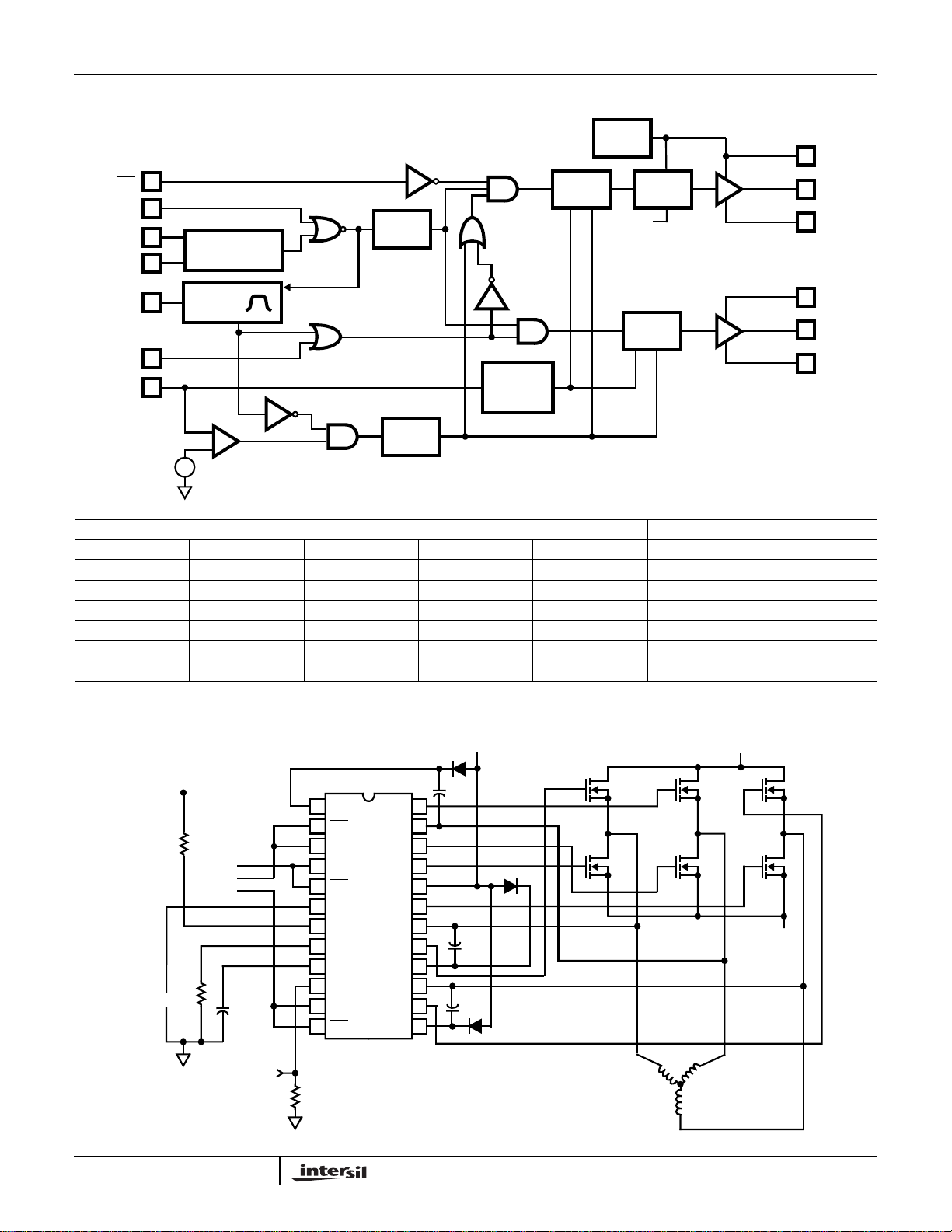
Functional Block Diagram
5
AHI
10
DIS
20
V
DD
UVLO
RFSH
ALI
RDEL
100mV
8
9
4
7
UNDERVOLTAGE
DETECTOR
RFSH
PULSE
-
+
+
V
SS
(1/3 of HIP4086 )
UV
INPUT OUTPUT
ALI, BLI, CLI
AHI, BHI, CHI UV DIS RDEL ALO, BLO, CLO AHO, BHO, CHO
XXX1X00
XX1XX00
1 X 0 0 >100mV 1 0
0000X01
0100X00
1 0 0 0 <100mV 1 1
NOTE: X signifies that input can be either a “1” or “0”.
10ns
DELAY
2µs
DELAY
DEAD TIME
CURRENT
MIRRORS
TRUTH TABLE
TURN-ON
DELAY
CHARGE
PUMP
SHIFTER
UV
DEAD TIME
DISABLE
TURN-ON
DELAY
LEVEL
DEAD TIME
DISABLE
DRIVER
DRIVER
AHB
16
AHO
17
AHS
18
V
20
DD
ALO
21
V
6
SS
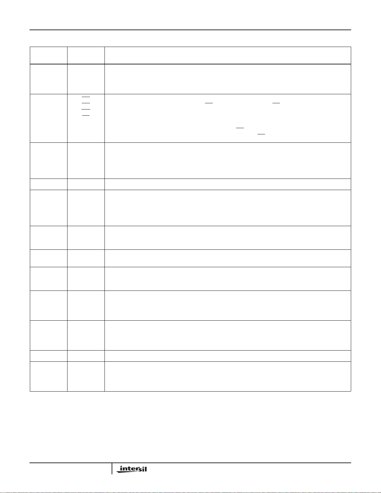
Typical Application
+12V
R
DEL
PWM
INPUTS
R
(OPTIONAL)
UV
C
RFSH
(OPTIONAL)
OPTIONAL
OVERCURRENT
LATCH
(PWM Mode Switching)
BHB
1
BHI
2
BLI
3
ALI
4
AHI
5
V
6
SS
7
RDEL
UVLO
8
RFSH
9
DIS
10
CLI
11
CHI
12
FROM
R
DIS
2
BHO
BHS
BLO
ALO
V
DD
CLO
AHS
AHO
AHB
CHS
CHO
CHB
+12V
24
23
22
21
20
19
18
17
16
15
14
13
3-PHASE
LOAD
80V
GND

HIP4086
HIP4086
Pin Descriptions
PIN
NUMBER SYMBOL DESCRIPTION
16
1
13
5
2
12
4
3
11
6VSSGround. Connect the sources of the Low-Side power MOSFETs to this pin.
7 RDEL Dead Time Setting. Connect a resistor from this pin to VDDto set timing current that defines the dead time
8 UVLO UndervoltageSetting. A resistor can be connected between this pin and VSSto program the undervoltage set
AHB
BHB
CHB
(xHB)
AHI
BHI
CHI
(xHI)
ALI
BLI
CLI
(xLI)
High-Side Bootstrap supplies. One external bootstrap diode and one capacitor are required for each. Connect
cathode of bootstrap diode and positive side of bootstrap capacitor to each xHB pin.
High-Side Logic Level Inputs. Logic at these three pins controls the three high side output drivers, AHO (Pin
17), BHO (Pin 24) and CHO (Pin 14). When xHI is low, xHO is high. When xHI is high, xHO is low. Unless the
dead time is disabled by connecting RDEL (Pin 7) to ground, the low side input of each phase will override the
corresponding high side input on that phase - see Truth Table on previous page. If RDEL is tied to ground,
dead time is disabled and the outputs follow the inputs. Care must be taken to avoid shoot-through in this application. DIS (Pin 10) also overrides the high side inputs. xHI can be driven by signal levels of 0V to 15V (no
greater than VDD). An internal 100µA pull-up to VDD will hold each xHI high if the pins are not driven.
Low-Side Logic Level Inputs. Logic at these three pins controls the three low side output drivers ALO (Pin 21),
BLO (Pin 22) and CLO (Pin 19). If the upper inputs are grounded then the lower inputs control both xLO and
xHO drivers, with the dead time set by the resistor at RDEL (Pin 7). DIS (Pin 10) high level input overrides xLI,
forcingall outputs low.xLI can be driven by signal levels of 0V to 15V (no greater than VDD). An internal 100µA
pull-up to VDD will hold xLI high if these pins are not driven.
between drivers - see Figure 15. All dr ivers turn-off with no adjustable delay,so the RDEL resistor guarantees
no shoot-through by delaying the turn-on of all drivers. When RDEL is tied to VSS, both upper and lowers can
be commanded on simultaneously.While not necessar y in most applications, a decoupling capacitor of 0.1µF
or smaller may be connected between RDEL and VSS.
point, see Figure 16. With this pin not connected, the undervoltage disable is typically 6.6V. When this pin is
tied to VDD, the undervoltage disable is typically 6.2V.
9 RFSH Refresh Pulse Setting. An external capacitor can be connected from this pin to VSSto increase the length of
the start up refresh pulse - see Figure 14. If this pin is not connected, the refresh pulse is typically 1.5µs.
10 DIS DisableInput.Logic levelinput thatwhen takenhigh sets all six outputs low.DIS high overridesall other inputs.
With DIS low, the outputs are controlled by the other inputs. DIS can be driven by signal levels of 0V to 15V
(no greater than VDD). An internal 100µA pull-up to VDD will hold DIS high if this pin is not driven.
17
24
14
15
23
15
20 V
21
22
19
NOTE: x = A, B and C.
AHO
BHO
CHO
(xHO)
AHS
BHS
CHS
(xHS)
DD
ALO
BLO
CLO
(xLO)
High-Side Outputs. Connect to the gates of the High-Side power MOSFETs in each phase.
High-Side Source Connection. Connect the sources of the High-SidepowerMOSFETsto these pins. The negative side of the bootstrap capacitors should also be connected to these pins.
Positive Supply. Decouple this pin to VSS (Pin 6).
Low-Side Outputs. Connect the gates of the Low-Side power MOSFETs to these pins.
3
 Loading...