Intersil Corporation HIP4020 Datasheet

June 1997
HIP4020
Half Amp Full Bridge Power Driver
for Small 3V, 5V and 12V DC Motors
Features
• Two Independent Controlled Complementary
MOS Power Output Half H-Drivers (Full-Bridge)
for Nominal 3V to 12V Power Supply Operation
• Split ±Voltage Power Supply Option for Output
Drivers
• Load Switching Capabilities to 0.5A
• Single Supply Range +2.5V to +15V
• Low Standby Current
• CMOS/TTL Compatible Input Logic
• Over-Temperature Shutdown Protection
• Over-Current Limit Protection
• Over-Current Fault Flag Output
• Direction, Braking and PWM Control
Applications
• DC Motor Driver
• Relay and Solenoid Drivers
• Stepper Motor Controller
• Air Core Gauge Instrument Driver
• Speedometer Displays
• Tachometer Displays
• Remote Power Switch
• Battery Operated Switch Circuits
• Logic and Microcontroller Operated Switch
Description
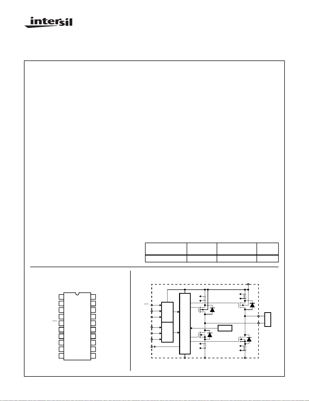
In the Functional Block Diagram of the HIP4020, the four switches
and a load are arranged in an H-Configuration so that the drive voltage from terminals OUTA and OUTB can be cross-switched to
change the direction of current flow in the load. This is commonly
known as 4-quadrant load control. As shown in the Block Diagram,
switches Q1 and Q4 are conducting or in an ON state when current
flows from V
nal V
SSB
through Q1 to the load, and then through Q4 to termi-
DD
; where load terminal OUTA is at a positive potential with
respect to OUTB. Switches Q1 and Q4 are operated synchronously
by the control logic. The control logic switches Q3 and Q2 to an open
or OFF state when Q1 and Q4 are switched ON. To reverse the current flow in the load, the switch states are reversed where Q1 and Q4
are OFF while Q2 and Q3 are ON. Consequently, current then flows
from V
V
SSA
through Q3, through the load, and through Q2 to terminal
DD
, and load terminal OUTB is then at a positive potential with
respect to OUTA.
Terminals ENA and ENB are ENABLE Inputs for the Logic A and B
Input Controls. The ILF output is an Over-Current Limit F ault Flag Output and indicates a fault condition for either Output A or B or both. The
V
and VSS are the Power Supply reference terminals for the A and
DD
B Control Logic Inputs and ILF Output. While the V
supply terminal is internally connected to each bridge driver , the V
and V
V
SS
Pow er Supply terminals are separate and independent from
SSB
and may be more negative than the VSS ground reference termi-
positive power
DD
SSA
nal. The use of level shifters in the gate drive circuitry to the NMOS
(low-side) output stages allows controlled level shifting of the output
drive relative to ground.
Ordering Information
TEMP.
PART NUMBER
HIP4020IB -40 to 85 20 Ld SOIC M20.3
RANGE (oC) PACKAGE PKG. NO.
Pinout
HIP4020 SOIC
TOP VIEW
1
NC
ILF
2
B2
3
ENB
4
B1
5
V
6
SS
ENA
7
8
A1
9
A2
NC
10
CAUTION: These devices are sensitive to electrostatic discharge; follow proper IC Handling Procedures.
http://www.intersil.com or 407-727-9207
NC
20
V
19
DD
NC
18
OUTB
17
V
16
SSB
V
15
SSA
OUTA
14
NC
13
12
V
DD
11
NC
| Copyright © Intersil Corporation 1999
Block Diagram
B1
B2
ENB
A1
A2
ENA
ILF
1
LOGIC B
CONTROL
LOGIC A
CONTROL
V
V
DD
I
T
SENSE
Q3
Q4
I
SENSE
SENSE
V
SSB
OUTB
OUTA
LOAD
I
SENSE
Q1
Q2
I
SENSE
LEVEL SHIFT, DRIVE CONTROL
OVER TEMP. AND CURRENT LIMIT,
SS
V
SSA
File Number 3976.1

HIP4020
Absolute Maximum Ratings Thermal Information
Supply Voltage; VDD to VSS or V
Neg. Output Supply Voltage, (V
DC Logic Input Voltage (Each Input) . . . (VSS -0.5V) to (VDD +0.5V)
DC Logic Input Current (Each Input) . . . . . . . . . . . . . . . . . . . . .±15mA
ILF Fault Output Current. . . . . . . . . . . . . . . . . . . . . . . . . . . . . . . .±15mA
Output Load Current, (Self Limiting, See Elec. Spec.). . . . .±I
SSA
SSA
or V
, V
. . . . . . . . . . . . . . +15V
SSB
). . . . . . . . . . . . . (Note 1)
SSB
O(LIMIT)
Thermal Resistance (Typical, Note 1) θ
Plastic SOIC Package. . . . . . . . . . . . . . . . . . . . . . . . . . 105oC/W
Maximum Storage Temperature Range . . . . . . . . . .-65oC to 150oC
Maximum Junction Temperature. . . . . . . . . . . . . . . . . . . . . . . 150oC
Maximum Lead Temperature (Soldering 10s). . . . . . . . . . . . . 300oC
(Lead Tips Only)
JA
Operating Conditions T
= 25oC
A
Typical Operating Supply Voltage Range, VDD. . . . . . . . +3 to +12V
Low Voltage Logic Retention, Min. VDD . . . . . . . . . . . . . . . . . . . +2V
Idle Supply Current; No Load, VDD = +5V . . . . . . . . . . . . . . . 0.8mA
Typical P+N Channel r
CAUTION: Stresses above those listed in “Absolute Maximum Ratings” may cause permanent damage to the device. This is a stress only rating and operation
of the device at these or any other conditions above those indicated in the operational sections of this specification is not implied.
, VDD = +5V, 0.5A Load . . . . . . . . . 2Ω
DS(ON)
NOTE:
1. θJA is measured with the component mounted on an evaluation PC board in free air.
Electrical Specifications T
= 25oC, VDD = +5V, V
A
SSA
= V
= VSS= 0V, Unless Otherwise Specified
SSB
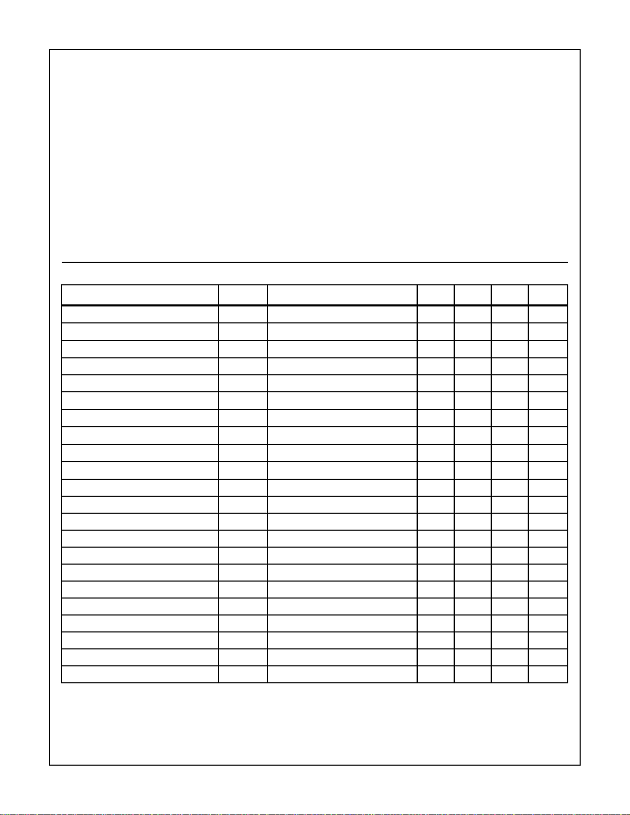
PARAMETER SYMBOL TEST CONDITIONS MIN TYP MAX UNITS
Input Leakage Current I
Low Level Input Voltage V
High Level Input Voltage V
ILF Output Low, Sink Current I
ILF Output High, Source Current I
Input Capacitance C
P-Channel r
N-Channel r
P-Channel r
N-Channel r
OUTA, OUTB Source Current Limiting I
OUTA, OUTB Sink Current Limiting -I
, Low Supply V oltage r
DS(ON)
, Low Supply V oltage r
DS(ON)
, High Supply Voltage r
DS(ON)
, High Supply Voltage r
DS(ON)
DS(ON)
DS(ON)
DS(ON)
DS(ON)
O(LIMIT)VDD
O(LIMIT)VDD
Idle Supply Current; No Load I
OUTA, OUTB Voltage High V
OUTA, OUTB Voltage Low V
OUTA, OUTB Voltage High V
OUTA, OUTB Voltage Low V
OUTA, OUTB Source Current Limiting I
OUTA, OUTB Sink Current Limiting -I
OUTA, OUTB Source Current Limiting I
OUTA, OUTB Sink Current Limiting -I
O(LIMIT)VDD
O(LIMIT)VDD
O(LIMIT)VDD
O(LIMIT)VDD
Thermal Shutdown T
LEAK
OH
OL
DD
VDD = +15V - - 25 nA
IL
IH
IN
V
SS
2
V
= 0.4V, VDD = +12V 15 - - mA
OUT
V
= 11.6V, VDD = +12V - - -15 mA
OUT
VDD = +3V, I
VDD= +3V, I
VDD= +12V, I
VDD= +12V, I
= +6V , VSS = 0V , V
= +6V , VSS = 0V , V
SOURCE
= 250mA
SINK
SOURCE
SINK
= 250mA
= 400mA
= 400mA
SSA
SSA
-
-
-
-
= V
= -6V 480 625 1500 mA
SS
B
= V
= -6V 480 800 1500 mA
SS
B
-
-
2-pF
1.6 2.1 Ω
1 1.5 Ω
0.6 1.2 Ω
0.5 1.1 Ω
- 0.8 1.5 mA
I
OH
OL
OH
OL
= 450mA 4.2 4.5 - V
SOURCE
I
= 450mA - 0.4 0.6 V
SINK
VDD= +3V, I
VDD = +3V, I
= 250mA 2.415 2.6 - V
SOURCE
= 250mA - 0.25 0.375 V
SINK
= +12V 480 625 1500 mA
= +12V 480 800 1500 mA
= +3V 480 625 1500 mA
= +3V 480 800 1500 mA
SD
- 145 -
0.8 V
V
DD
V
o
C
2

HIP4020
Electrical Specifications T
= 25oC, VDD = +5V, V
A
SSA
= V
= VSS= 0V, Unless Otherwise Specified (Continued)
SSB
PARAMETER SYMBOL TEST CONDITIONS MIN TYP MAX UNITS
t
r
t
f
IO = 0.5A (Note 2)
- 2.5 - µs
-4-µs
- 0.1 - µs
- 0.1 - µs
Response Time: VEN to V
Turn-On: Prop Delay
Rise Time
Turn-Off: Prop Delay
Fall Time
OUT
t
PLH
t
PHL
NOTES:
is the required common ground reference for the logic input switching. The load currents may be switched positive and negativ e in
1. V
SS
reference to the VSS common ground by using a split supply for VDD (positive) to V
supply voltage, the Maximum Negative Output Supply Voltage for V
SSA
and V
SSB
SSA
and V
(negative). For an uneven split in the
SSB
is limited by the Maximum VDD to V
SSA
or V
SSB
Since the VDD pins are internally tied together, the voltage on each VDD pins must be equal and common.
2. Refer to the Truth Table and the VEN to V
Switching Waveforms. Current, IO refers to I
OUT
OUT A
or I
as the Output Load current. Note
OUTB
that ENA controls OUTA and ENB controls OUTB. Each Half H-Switch has independent control from the respective A1, A2, ENA or B1,
B2, ENB inputs. Refer to the Terminal Information Table for external pin connections to establish mode control switching. Figure 1 shows
a typical application circuit used to control a DC Motor.
Pin Descriptions
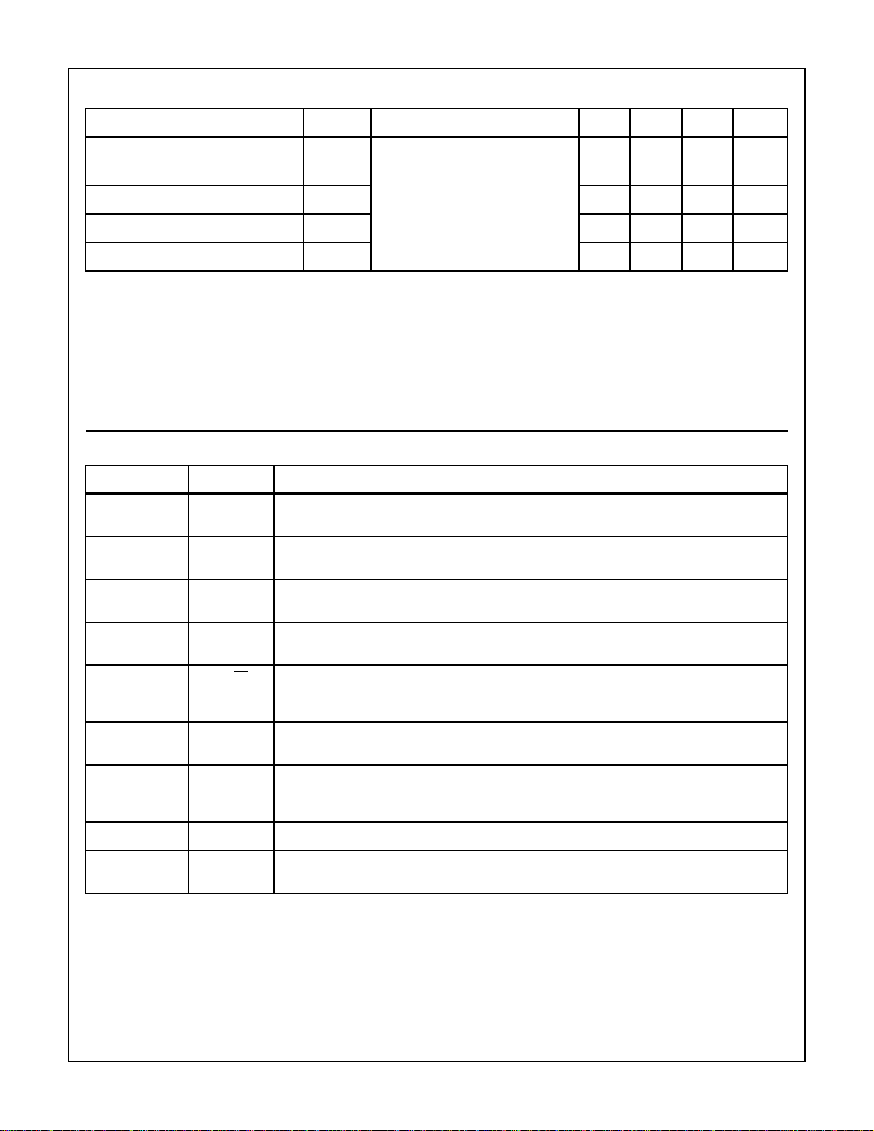
PIN NUMBER SYMBOL DESCRIPTION
ratings.
12, 19 V
DD
Positive Power Supply pins; internally common and externally connect to the same Positive Supply
(V+).
15 V
SSA
Negative Power Supply pin; Negative or Ground return for Switch Driver A; externally connect to the
Supply (V-).
16 V
SSB
Negative Power Supply pin; Negative or Ground return for Switch Driver B; externally connect to the
Supply (V-).
6V
SS
Common Ground pin for the Input Logic Control circuits. May be used as a common ground with
V
and V
SSA
SSB.
8, 5 A1, B1 Input pins used to control the direction of output load current to/from OUTA and OUTB, respectively.
When connected, A1 and B1 can be controlled from the same logic signal to change the directional
rotation of a motor.
9, 3 A2, B2 Input pins used to force a low state on OUTA and OUTB, respectively. When connected, A2 and B2
can be controlled from the same logic signal to activate Dynamic Braking of a motor.
7, 4 ENA, ENB Input pins used to Enable Switch Driver A and Switch Driver B, respectively. When Low, the respec-
tive output is in a high impedance (Z) off-state. Since each Switch Driver is independently controlled,
OUTA and OUTB may be a separately PWM controlled as Half H-Switch Drivers.
14, 17 OUTA, OUTB Respectively, Switch Driver A and Switch Driver B Output pins.
2 ILF Current Limiting Fault Output Flag pin; when in a high logic state, signifies that Switch Driver A or B
or both are in a Current Limiting Fault Mode.
3
 Loading...