Intersil Corporation HIP4011 Datasheet

HIP4011
April 1994
Three Phase Brushless DC Motor Controller
Features
• 3A DC, 5A Peak Output Current
• 16V Max. Rated Supply Voltage
[ /Title (HIP4011)
• Built-in “Free-Wheeling” Diodes
/Subject (Three Phase Brushless DC Motor Controller)
• Output dv/dt Limited to Reduce EMI
/Author ()
• External Dynamic Brake Control Switch With
/Keywords ()
Undervoltage Sense
/Creator ()
• Thermal and Current Limiting Protects Against
/DOCINFO pdfmark
Locked Rotor Conditions
• Provides Analog Current Sense and Reference Inputs
[ /PageMode /UseOutlines
/DOCVIEW pdfmark
• Decode Logic with Illegal Code Rejection
Applications
• Drive Spindle Motor Controller
• 3 Phase Brushless DC Motor Controller
• Brushless DC Motor Driver for 12V Battery Powered
Appliances
• Phased Driver for 12V DC Applications
Description
The HIP401 1 motor driver is intended for three phase Brushless motor control at continuous output currents up to 3A. It
accepts inputs from buffered Hall effect sensors and drives
three motor windings, regulating the current through an
external current sensing resistor, according to an analog
control input. Output “freewheeling” diodes are built in and
output dv/dt is limited to decrease the generated EMI.
Thermal and current limiting are used to protect the device
from locked rotor conditions. A brake control input forces all
outputs to ground simultaneously to provide dynamic
braking, and an internal voltage sensor does the same when
the supply drops below a predetermined switch point. Power
down braking energy is stored in an external capacitor.
Ordering Information
PART
NUMBER
HIP4011IS -40oC to +85oC 15 Pin Plastic SIP
TEMPERATURE
RANGE PACKAGE
Surface Mount
• Logic Controlled Driver for Solenoids, Relays and
Lamps
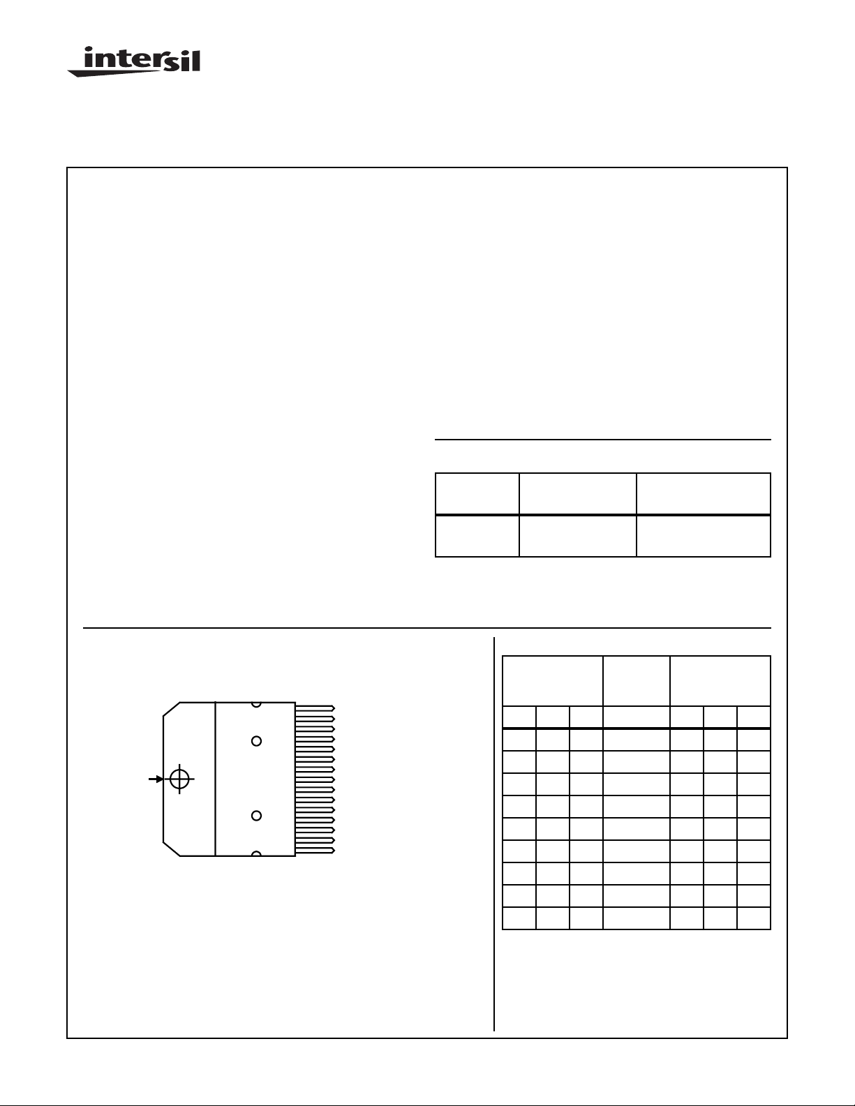
Pinout
HIP4011 (SIP)
TOP VIEW
PGND PIN
(TAB) MUST BE
ELECTRICALLY
CONNECTED
15
14
13
12
11
10
9
8
7
6
5
4
3
2
1
SGND = SIGNAL GROUND
SPD = SPEED CONTROL
SV+ = SIGNAL V+
ISEN = ISENSE
OUTA = OUTPUT A
BCAP = BRAKING CAPACITOR
PV+ = POWER V+
OUTB = OUTPUT B
ISEN = ISENSE
FBRK = FORCED BRAKE
OUTC = OUTPUT C
PV+ = POWER V+
SENC = SENSE INPUT C
SENB = SENSE INPUT B
SENA = SENSE INPUT A
OUTPUT TRUTH TABLE
FORCE
SENSOR
INPUTS
A B C FBRK A B C
0 0 0 0 OFF OFF OFF
1 0 0 0 1 OFF 0
010001OFF
110 0 OFF10
001 0 OFF01
101010OFF
0 1 1 0 0 OFF 1
1 1 1 0 OFF OFF OFF
XXX 1 000
* Undervoltage and Force Brake logic truth table
entries are identical.
“X” = Don’t Care
BRAKE
INPUT* OUTPUTS
CAUTION: These devices are sensitive to electrostatic discharge; follow proper IC Handling Procedures.
407-727-9207
| Copyright © Intersil Corporation 1999
6-11
File Number
2939.3

Specifications HIP4011
Absolute Maximum Ratings Thermal Information
Supply Voltage, SV+ or PV+. . . . . . . . . . . . . . . . . . . . . .-1V to +16V
Referred to SGND or PGND (Note 1)
Output Current, Continuous . . . . . . . . . . . . . . . . . . . . . . . . . . . . . 3A
Output Current, Peak (Note 2) . . . . . . . . . . . . . . . . . . . . . . . . . . . 5A
Substrate (PGND) Current . . . . . . . . . . . . . . . . . . . . . . . . . . . . . . 1A
Logic Input Current. . . . . . . . . . . . . . . . . . . . . . . . .-20mA to +20mA
(Clamped to SV+ and SGND)
NOTES:
1. PV+ and SV+ are to be tied together, as are PGND and SGND.
2. Operating above the continuous current rating causes a decrease in operating life.
3. Derate power dissipation above case temperature of +75
CAUTION: Stresses above those listed in “Absolute Maximum Ratings” may cause permanent damage to the device. This is a stress only rating and operation
of the device at these or any other conditions above those indicated in the operational sections of this specification is not implied.
o
C at 0.33 Watts/oC.
Thermal Resistance θ
JA
θ
JC
15 Lead SIP Power Package. . . . . . . . . . 45oC/W 3oC/W
Power Dissipation (Note 3) . . . . . . . . . . . . . . . . . . . . . . . . . . . . 25W
Junction Temperature Range, Operating . . . . . . . . . . . . . . . +150oC
Storage Temperature Range. . . . . . . . . . . . . . . . . .-55oC to +150oC
Power Dissipation
Up to +125oC without heat sink. . . . . . . . . . . . . . . . . . . . . 0.56W
Above +125oC without Heat Sink . . Derate Linearly at 22mW/oC
Up to +125oC with Infinite Heat Sink. . . . . . . . . . . . . . . . . 8.33W
Above +125oC with Infinite Heat Sink . . . . . . . . . . . . . . . . . . . . . .
. . . . . . . . . . . . . . . . . . . . . . . . . . . . .Derate Linearly at 333mW/oC
Lead Temperature (During Soldering)
At a Distance 1/16 inch ±1/32 inch (1.59mm ±0.79mm)
from Case for 10s Max. . . . . . . . . . . . . . . . . . . . . . . . . . +265oC
Electrical Specifications T
= +25oC and SV+ = PV+ = 10.4V to 13.2V, Unless Otherwise Specified
A
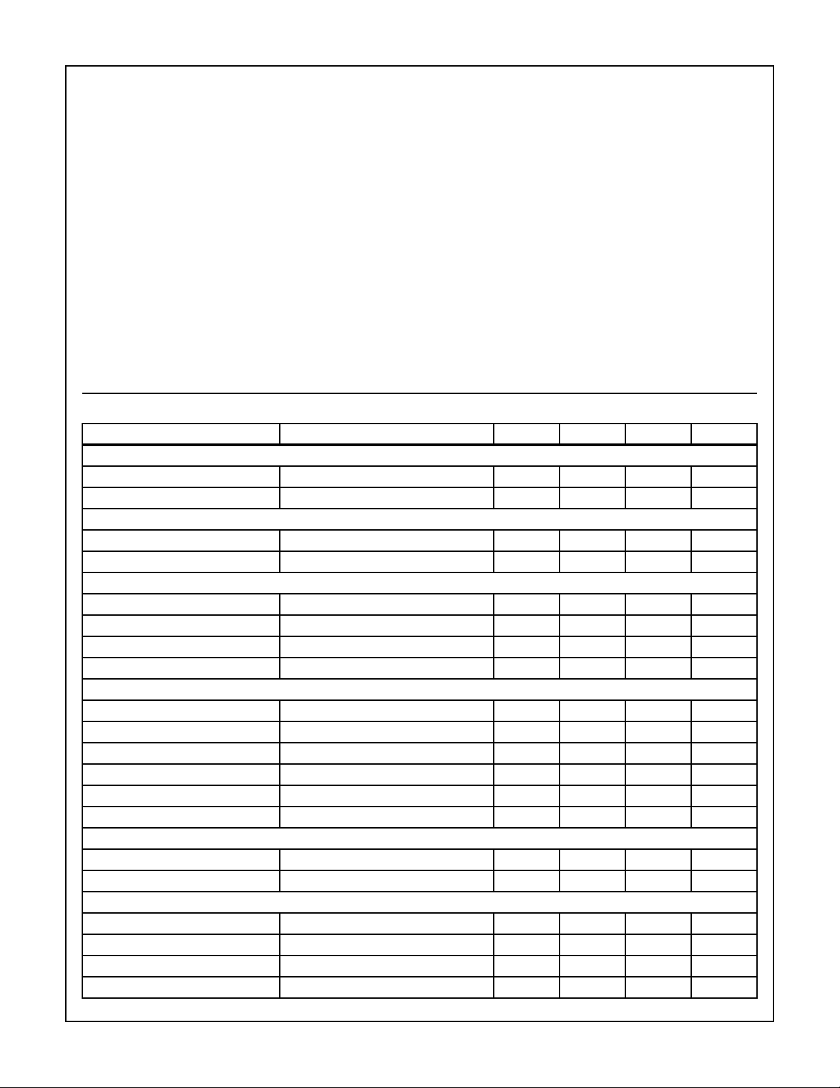
PARAMETERS TEST CONDITION MIN TYP MAX UNITS
SUPPLY (SV+) CURRENT
No Drive Outputs Off - - 10 mA
With Drive Outputs On - - 15 mA
LOGIC INPUT CURRENT
Sensor Inputs SENA, SENB & SENC = 0V to 3V -0.5 - -1.5 mA
Brake Input FBRK = 0.8V to 2.4V 50 - 150 µA
LOGIC INPUT THRESHOLDS
Sensor Inputs Logic “0” Input Voltage - - 1.8 V
Sensor Inputs Logic “1” Input Voltage 3 - - V
Brake Input Logic “0” Input Voltage - - 0.8 V
Brake Input Logic “1” Input Voltage 2.4 - - V
AMPLIFIER INPUT (SPD)
Bias Current - - 700 nA
Offset Voltage --3mV
Input Range (Linear) 0 - 1 V
Input Impedance 1--MΩ
System Bandwidth (Note 1) - 35 - kHz
Current Limit Rsense = 0.20Ω -5-A
THERMAL LIMIT
o
Threshold - 155 -
C
Hysteresis -40-oC
OUTPUT DRIVERS
On Saturation (See Note 5) I
On Saturation (See Note 5) I
Off Leakage PV+ > V
= 3A, V
OUT
= 0.6A, V
OUT
PMOS
PMOS
> PGND or I
OUT
+ V
+ V
NMOS
NMOS
SEN
- - 2.2 V
- - 0.44 V
--1mA
Slew Rate (See Note 2) - 0.5 - V/µS
6-12
 Loading...