

Intersil Corporation HIP2106 Datasheet

HIP2106
Data Sheet August 1999 File Number
100V/1A Peak, Low Cost, High Frequency
Half Bridge Driver
The HIP2106 is a high frequency, 100V Half Bridge
N-Channel MOSFET driver IC, av ailable in 8 lead plastic
SOIC. The low-side and high-side gate drivers are
independently controlled and matched to 8ns. This gives the
user maximum flexibility in dead-time selection and driver
protocol. Undervoltage protection on both the low-side and
high-side supplies force the outputs low. An on-chip diode
eliminates the discrete diode required with other driver ICs. A
new levelshifter topology yields the low-power benefits of
pulsed operation with the safetyofDCoperation.Unlikesome
competitors, the high-side output returns to its correct state
after a momentary undervoltage of the high-side supply.
Ordering Information
TEMP.
PART NUMBER
HIP2106IB -40 to 85 8 Ld SOIC M8.15
HIP2106IP -40 to 85 8 Ld PDIP E8.3
RANGE (oC) PACKAGE
PKG.
NO.
Pinout
HIP2106 (SOIC, PDIP)
TOP VIEW
1
V
DD
HB
2
HO
3
HS
4
8
LO
V
7
SS
LI
6
HI
5
4406.2
Features
• Drives N-Channel MOSFET Half Bridge
• Space Saving SO8 Package
• Bootstrap Supply Max Voltage to 116V
DC
• On-Chip 1Ω Bootstrap Diode
• Fast Propagation Times Needed for Multi-MHz Circuits
• Drives 1000pF Load at 500kHz with Rise and Fall Times
of Typically 20ns
• CMOS Input Thresholds for Improved Noise Immunity
• Independent Inputs for Non-Half Bridge Topologies
• No Start-Up Problems
• Outputs UnaffectedbySupplyGlitches,HSRingingBelow
Ground, or HS Slewing at High dv/dt
• Low Power Consumption
• Wide Supply Range
• Supply Undervoltage Protection
•3Ω Output Resistance
Applications
• Telecom Half Bridge Power Supplies
• Avionic DC-DC Converters
• Two-Switch Forward Converters
• Active Clamp Forward Converters
Application Block Diagram
PWM
CONTROLLER
1
+12V
+100V
V
DD
HB
SECONDARY
CIRCUIT
HI
LI
DRIVE
HI
DRIVE
CONTROL
LO
HIP2106
V
SS
CAUTION: These devices are sensitive to electrostatic discharge; follow proper IC Handling Procedures.
HO
HS
LO
REFERENCE
AND
ISOLATION
http://www.intersil.com or 407-727-9207 | Copyright © Intersil Corporation 1999
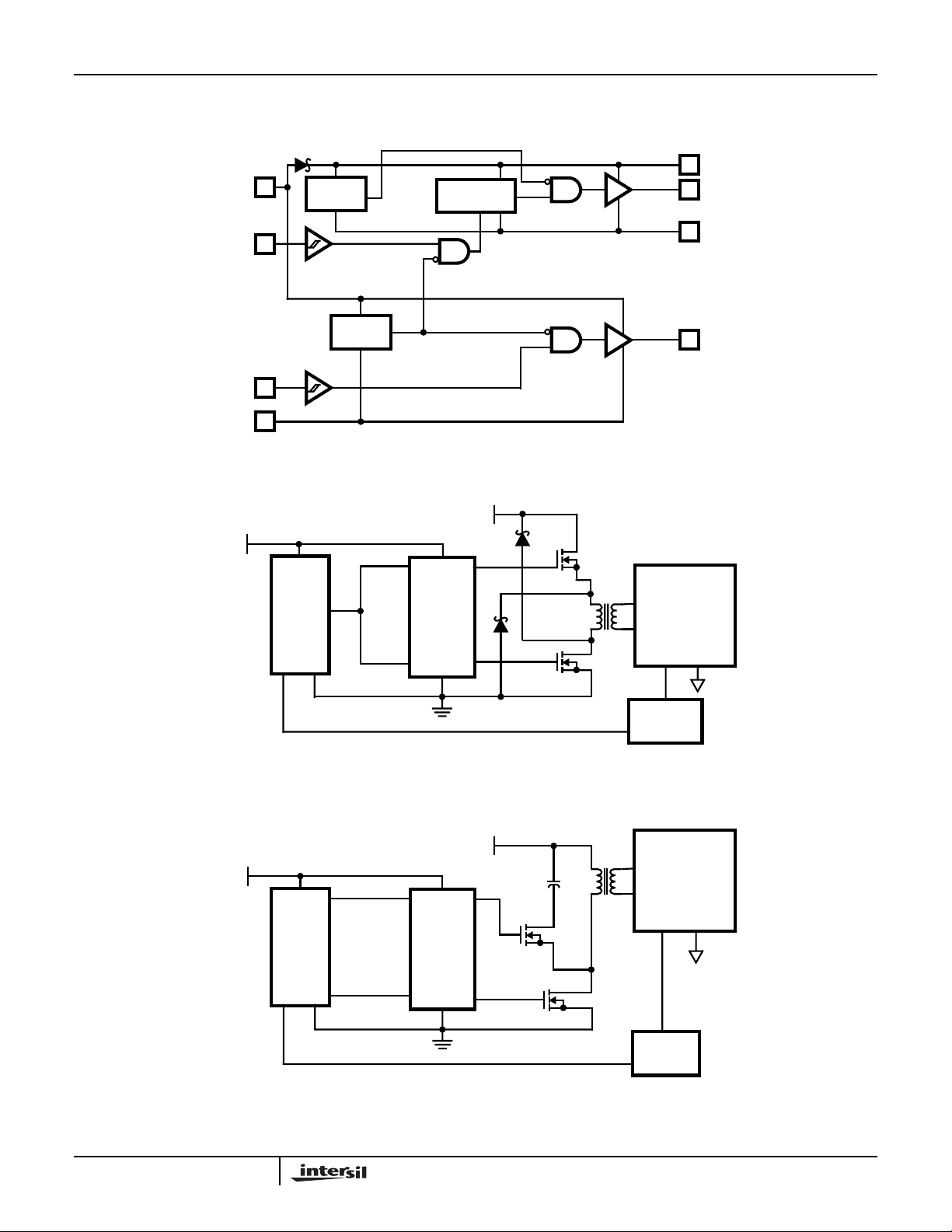
Functional Block Diagram
1
V
DD
5
HI
6
LI
7
V
SS
Other Applications
UNDER
VOLTAGE
UNDER
VOLTAGE
HIP2106
LEVEL SHIFT
DRIVER
DRIVER
2
HB
3
HO
4
HS
8
LO
+12V
+12V
+48V
PWM
HIP
2106
FIGURE 1. TWO-SWITCH FORWARD CONVERTER
+48V
PWM
HIP
2106
SECONDARY
CIRCUIT
ISOLATION
SECONDARY
CIRCUIT
FIGURE 2. FORWARD CONVERTER WITH AN ACTIVE CLAMP
2
ISOLATION

HIP2106
Absolute Maximum Ratings Thermal Information
Supply Voltage, V
DD,VHB-VHS
LI and HI Voltages . . . . . . . . . . . . . . . . . . . . . . . . .-3V to VDD +0.3V
Voltage on LO . . . . . . . . . . . . . . . . . . . . . . . . . . -0.3V to VDD +0.3V
Voltage on HO . . . . . . . . . . . . . . . . . . . . . . VHS -0.3V to VHB +0.3V
Voltage on HS (Continuous) . . . . . . . . . . . . . . . . . . . . . -1V to 110V
Voltage on HB . . . . . . . . . . . . . . . . . . . . . . . . . . . . . . . . . . . . +118V
Average Current in VDD to HB Diode. . . . . . . . . . . . . . . . . . . 100mA
ESD Classification . . . . . . . . . . . . . . . . . . . . . . . . . . . . Class 1 (1kV)
Recommended Operating Conditions
Supply Voltage, VDD . . . . . . . . . . . . . . . . . . . . . . . . . +9V to +16.5V
Voltage on HS . . . . . . . . . . . . . . . . . . . . . . . . . . . . . . . . -1V to 100V
CAUTION: Stresses above those listed in “Absolute Maximum Ratings” may cause permanent damage to the device. This is a stress only rating and operationofthe
device at these or any other conditions above those indicated in the operational sections of this specification is not implied.
NOTES:
1. θJA is measured with the component mounted on an evaluation PC board in free air.
2. All Voltages Relative to Pin 4, VSS Unless Otherwise Specified.
Electrical Specifications VDD= VHB= 12V, VSS= VHS= 0V, No Load on LO or HO, Unless Otherwise Specified
PARAMETER SYMBOL TEST CONDITIONS
SUPPLY CURRENTS
VDD Quiescent Current I
VDD Operating Current I
Total HB Quiescent Current I
Total HB Operating Current I
HB to VSS Current, Quiescent I
HB to VSS Current, Operating I
INPUT PINS
Low Level Input Voltage Threshold V
High Level Input Voltage Threshold V
Input Voltage Hysteresis V
Input Pulldown Resistance R
UNDER VOLTAGE PROTECTION
VDD Rising Threshold V
VDD Threshold Hysteresis V
HB Rising Threshold V
HB Threshold Hysteresis V
BOOT STRAP DIODE
Low-Current Forward Voltage V
High-Current Forward Voltage V
Dynamic Resistance R
LO GATE DRIVER
Low Level Output Voltage V
High Level Output Voltage V
Peak Pullup Current I
Peak Pulldown Current I
HO GATE DRIVER
Low Level Output Voltage V
High Level Output Voltage V
Peak Pullup Current I
. . . . . . . . . . . . . . . . . . .-0.3V to 18V
DD
DDO
HB
HBO
HBS
HBSO
IHYS
DDR
DDH
HBR
HBH
DH
OLL
OHL
OHL
OLL
OLH
OHH
OHH
LI = HI = 0V - 0.1 0.15 - 0.2 mA
f = 500kHz - 1.5 2.5 - 3 mA
LI = HI = 0V - 0.1 0.15 - 0.2 mA
f = 500kHz - 1.5 2.5 - 3 mA
VHS = VHB = 116.5V - 0.05 1 - 10 µA
f = 500kHz - 0.7 - - - mA
IL
IH
I
I
DL
D
= 100µA - 0.45 0.55 - 0.7 V
VDD-HB
I
= 100mA - 0.7 0.8 - 1 V
VDD-HB
I
= 100mA - 0.8 1 - 1.5 Ω
VDD-HB
ILO = 100mA - 0.25 0.3 - 0.4 V
ILO = -100mA, V
VLO = 0V - 1 - - - A
VLO = 12V - 1 - - - A
IHO = 100mA - 0.25 0.3 - 0.4 V
IHO = -100mA, V
VHO = 0V - 1 - - - A
Thermal Resistance (Typical, Note 1) θJA (oC/W)
SOIC Package . . . . . . . . . . . . . . . . . . . . . . . . . . . . . 160
PDIP Package . . . . . . . . . . . . . . . . . . . . . . . . . . . . . 100
HS Slew Rate. . . . . . . . . . . . . . . . . . . . . . . . . . . . . . . . . . . 10V/ns
Maximum Power Dissipation at 25oC in Free Air. . . . . . . . . .780mW
Maximum Storage Temperature Range. . . . . . . . . . -65oC to 150oC
Maximum Junction Temperature Range . . . . . . . . . -55oC to 150oC
Maximum Lead Temperature (Soldering 10s) . . . . . . . . . . . . .300oC
(Lead Tips Only)
Voltage on HS . . . . . . . . . . . . . . . (Repetitive Transient) -5V to 105V
Voltage on HB. . .VHS +8V to VHS+16.5V and VDD-1V to VDD+100V
TJ= -40oC
TJ = 25oC
TO 125oC
4 5.4 - 3 - V
- 5.8 8 - 9 V
- 0.4 - - - V
- 200 - 100 500 kΩ
7 7.3 8 6.5 8.5 V
- 0.5 - - - V
6.5 6.9 7.5 6 8 V
- 0.4 - - - V
OHL
OHH
= VDD-V
= VHB-V
LO
HO
- 0.25 0.3 - 0.4 V
- 0.25 0.3 - 0.4 V
UNITSMIN TYP MAX MIN MAX
3
 Loading...