

HIP2100
Data Sheet October 1998 File Number 4022.2
100V/2A Peak, Low Cost, High Frequency
Half Bridge Driver
The HIP2100 is a high frequency, 100V Half Bridge
N-Channel MOSFET driver IC, available in 8 lead plastic
SOIC. The low-side and high-side gate drivers are
independently controlled and matched to 8ns. This gives the
user maximum flexibility in dead-time selection and driver
protocol. Undervoltage protection on both the low-side and
high-side supplies force the outputs low. An on-chip diode
eliminates the discrete diode required with other driver ICs.
A new level-shifter topology yields the low-power benefits of
pulsed operation with the safety of DC operation. Unlike
some competitors, the high-side output returns to its correct
state after a momentary undervoltage of the high-side
supply.
Ordering Information
TEMP.
PART NUMBER
HIP2100IB -40oC to 85oC 8 Ld SOIC (N) M8.15
RANGE (oC) PACKAGE PKG. NO.
Features
• Drives N-Channel MOSFET Half Bridge
• Space Saving SO8 Package
• Bootstrap Supply Max Voltage to 116VDC
• On-Chip 1Ω Bootstrap Diode
• Fast Propagation Times Needed for Multi-MHz Circuits
• Drives 1000pF Load at 1MHz with Rise and Fall Times of
Typically 10ns
• CMOS Input Thresholds for Improved Noise Immunity
• Independent Inputs for Non-Half Bridge Topologies
• No Start-Up Problems
• Outputs Unaffectedby Supply Glitches,HSRinging Below
Ground, or HS Slewing at High dv/dt
• Low Power Consumption
• Wide Supply Range
• Supply Undervoltage Protection
•3Ω Output Resistance
Applications
• Telecom Half Bridge Power Supplies
• Avionic DC-DC Converters
• Two-Switch Forward Converters
• Active Clamp Forward Converters
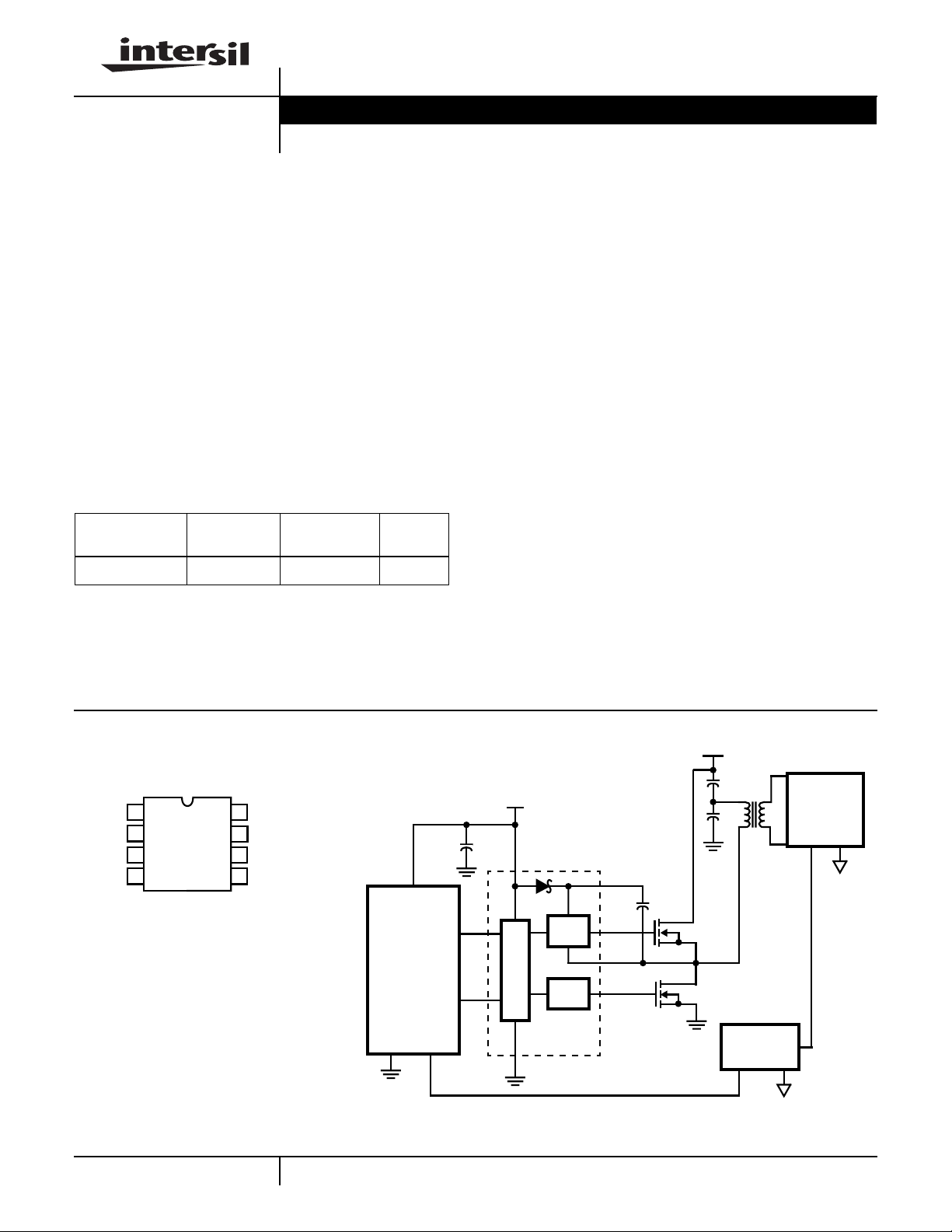
Pinout
V
DD
HB
HO
HS
HIP2100 (SOIC)
TOP VIEW
1
2
3
4
Application Block Diagram
+100V
+12V
8
LO
V
7
SS
LI
6
HI
5
HI
PWM
CONTROLLER
1
CAUTION: These devices are sensitive to electrostatic discharge; follow proper IC Handling Procedures.
LI
V
DD
HB
DRIVE
HI
DRIVE
CONTROL
LO
HIP2100
V
SS
http://www.intersil.com or 407-727-9207
HO
HS
LO
REFERENCE
ISOLATION
| Copyright © Intersil Corporation 1999
AND
SECONDARY
CIRCUIT
Functional Block Diagram
1
V
DD
5
HI
6
LI
7
V
SS
Other Applications
UNDER
VOLTAGE
UNDER
VOLTAGE
HIP2100
LEVEL SHIFT
DRIVER
DRIVER
2
HB
3
HO
4
HS
8
LO
+12V
+12V
+48V
PWM
HIP
2100
FIGURE 1. TWO-SWITCH FORWARD CONVERTER
+48V
PWM
HIP
2100
SECONDARY
CIRCUIT
ISOLATION
SECONDARY
CIRCUIT
FIGURE 2. FORWARD CONVERTER WITH AN ACTIVE CLAMP
2
ISOLATION
HIP2100
Absolute Maximum Ratings Thermal Information
Supply Voltage, V
DD,VHB-VHS
LI and HI Voltages . . . . . . . . . . . . . . . . . . . . . . . . -3V to VDD +0.3V
Voltage on LO . . . . . . . . . . . . . . . . . . . . . . . . . . -0.3V to VDD +0.3V
Voltage on HO . . . . . . . . . . . . . . . . . . . . . . VHS -0.3V to VHB +0.3V
Voltage on HS (Continuous) . . . . . . . . . . . . . . . . . . . . . -1V to 110V
Voltage on HB . . . . . . . . . . . . . . . . . . . . . . . . . . . . . . . . . . . . +118V
Average Current in VDD to HB diode. . . . . . . . . . . . . . . . . . . 100mA
ESD Classification . . . . . . . . . . . . . . . . . . . . . . . . . . . Class 1 (1kV)
NOTE: AllVoltagesRelativetoPin7,VSSUnlessOtherwise Specified
CAUTION: Stresses above those listed in “Absolute Maximum Ratings” may cause permanent damage to the device. This is a stress only rating and operationofthe
device at these or any other conditions above those indicated in the recommended operating conditions of this specification is not implied.
Recommended Operating Conditions
Supply Voltage, VDD . . . . . . . . . . . . . . . . . . . . . . . . . +9V to +16.5V
Voltage on HS . . . . . . . . . . . . . . . . . . . . . . . . . . . . . . . . -1V to 100V
. . . . . . . . . . . . . . . . . . -0.3V to 18V
Thermal Resistance θ
JA
θ
JC
SOIC . . . . . . . . . . . . . . . . . . . . . . . . . . . . 160oC/W N/A
SOIC in Thermal Conductive Media. . . . . . . . . . . . . . . . . 70oC/W
HS Slew Rate . . . . . . . . . . . . . . . . . . . . . . . . . . . . . . . . . . . . 10V/ns
Storage Temperature Range . . . . . . . . . . . . . . . . . . -65oC to 150oC
Junction Temperature Range. . . . . . . . . . . . . . . . . . -55oC to 150oC
Lead Temperature (Soldering 10s - Lead Tips Only). . . . . . . 300oC
Maximum Power Dissipation at +25oC in Free Air. . . . . . . . 780mW
Voltage on HS . . . . . . . . . . . . . . . (Repetitive Transient) -5V to 105V
Voltage on HB VHS +8V to VHS +16.5V and VDD -1V to VDD+100V
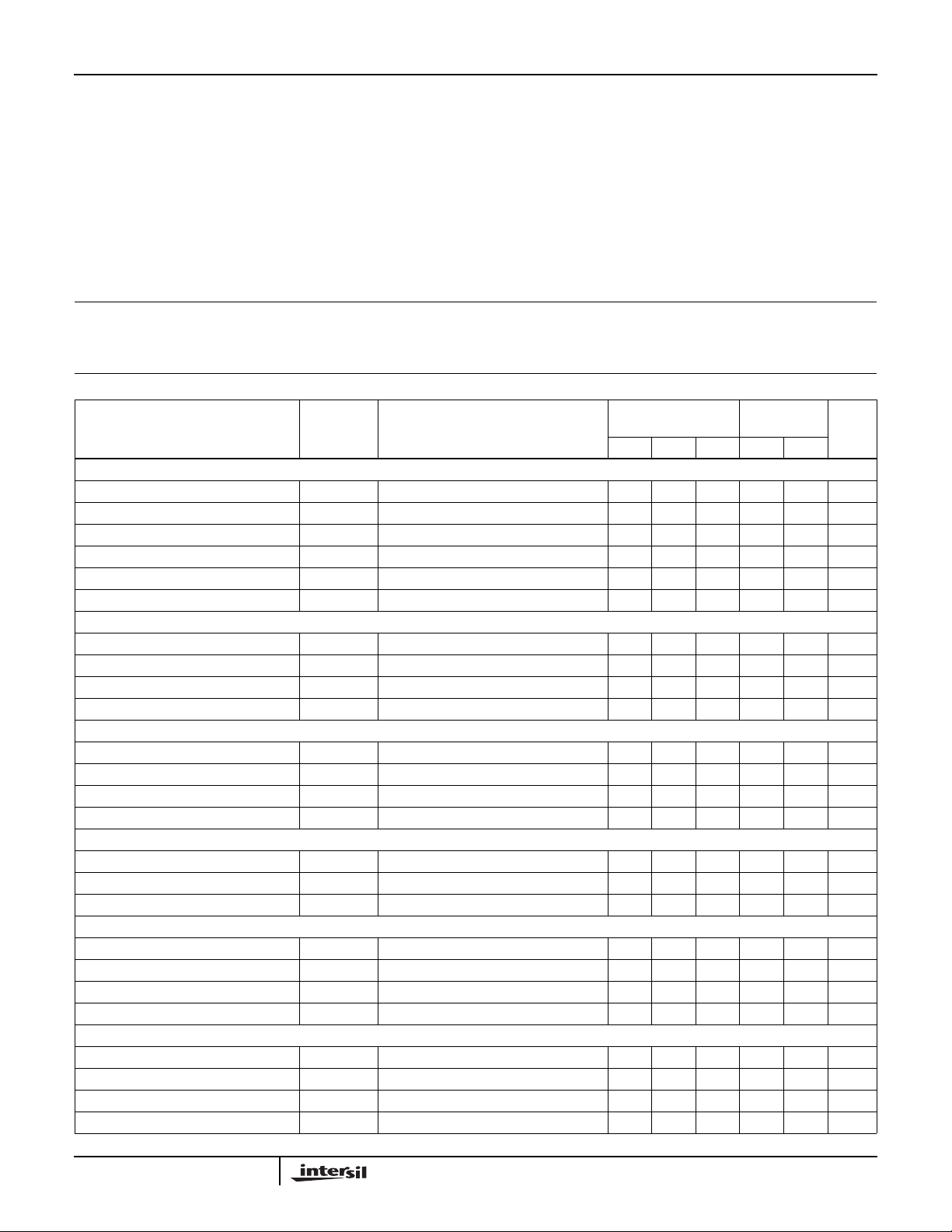
Electrical Specifications V
= VHB= 12V, VSS= VHS= 0V, No Load on LO or HO, Unless Otherwise Specified
DD
PARAMETERS SYMBOL TEST CONDITIONS
SUPPLY CURRENTS
VDD Quiescent Current I
VDD Operating Current I
Total HB Quiescent Current I
Total HB Operating Current I
HB to VSS Current, Quiescent I
HB to VSS Current, Operating I
INPUT PINS
Low Level Input Voltage Threshold V
High Level Input Voltage Threshold V
Input Voltage Hysteresis V
Input Pulldown Resistance R
UNDER VOLTAGE PROTECTION
VDD Rising Threshold V
VDD Threshold Hysteresis V
HB Rising Threshold V
HB Threshold Hysteresis V
BOOT STRAP DIODE
Low-Current Forward Voltage V
High-Current Forward Voltage V
Dynamic Resistance R
LO GATE DRIVER
Low Level Output Voltage V
High Level Output Voltage V
Peak Pullup Current I
Peak Pulldown Current I
HO GATE DRIVER
Low Level Output Voltage V
High Level Output Voltage V
Peak Pullup Current I
Peak Pulldown Current I
DD
DDO
HB
HBO
HBS
HBSO
IL
IH
IHYS
I
DDR
DDH
HBR
HBH
DL
DH
D
OLL
OHL
OHL
OLL
OLH
OHH
OHH
OLH
TJ= - 40oC
TJ = 25oC
TO 125oC
UNITSMIN TYP MAX MIN MAX
LI = HI = 0V - 0.1 0.15 - 0.2 mA
f = 500kHz - 1.5 2.5 - 3 mA
LI = HI = 0V - 0.1 0.15 - 0.2 mA
f = 500kHz - 1.5 2.5 - 3 mA
VHS = VHB = 116.5V - 0.05 1 - 10 µA
f = 500kHz - 0.7 - - - mA
4 5.4 - 3 - V
- 5.8 7 - 8 V
- 0.4 - - - V
- 200 - 100 500 kΩ
7 7.3 7.8 6.5 8 V
- 0.5 - - - V
6.5 6.9 7.5 6 8 V
- 0.4 - - - V
I
= 100µA - 0.45 0.55 - 0.7 V
VDD-HB
I
= 100mA - 0.7 0.8 - 1 V
VDD-HB
I
= 100mA - 0.8 1 - 1.5 Ω
VDD-HB
ILO = 100mA - 0.25 0.3 - 0.4 V
ILO = -100mA, V
OHL
= VDD-V
LO
- 0.25 0.3 - 0.4 V
VLO = 0V - 2 - - - A
VLO = 12V - 2 - - - A
IHO = 100mA - 0.25 0.3 - 0.4 V
IHO = -100mA, V
OHH
= VHB-V
HO
- 0.25 0.3 - 0.4 V
VHO = 0V - 2 - - - A
VHO = 12V - 2 - - - A
3

HIP2100
Switching Specifications VDD = VHB = 12V, VSS = VHS = 0V, No Load on LO or HO, Unless Otherwise Specified
TJ = 25oC
- 20 35 - 45 ns
- 20 35 - 45 ns
- 20 35 - 45 ns
- 20 35 - 45 ns
- 2 8 - 10 ns
- 2 8 - 10 ns
----50ns
-10---ns
PARAMETERS SYMBOL
Lower Turn-Off Propagation Delay (LI Falling to LO Falling) t
Upper Turn-Off Propagation Delay (HI Falling to HO Falling) t
Lower Turn-On Propagation Delay (LI Rising to LO Rising) t
Upper Turn-On Propagation Delay (HI Rising to HO Rising) t
Delay Matching: Lower Turn-On and Upper Turn-Off t
Delay Matching: Lower Turn-Off and Upper Turn-On t
Either Output Rise/Fall Time t
LPHL
HPHL
LPLH
HPLH
MON
MOFF
RC,tFC
Either Output Rise/Fall Time (3V to 9V) tR,t
Either Output Rise Time Driving DMOS t
Either Output Fall Time Driving DMOS t
Minimum Input Pulse Width that Changes the Output t
Bootstrap Diode Turn-On or Turn-Off Time t
RD
FD
PW
BS
TEST
CONDITIONS
CL= 1000pF - 10 - - - ns
CL= 0.1µF - 0.5 0.6 - 0.8 us
F
CL= IRFR120 - 20 - - - ns
CL= IRFR120 - 10 - - - ns
Pin Descriptions
TJ = - 40oC
TO 125oC
UNITSMIN TYP MAX MIN MAX
PIN
NUMBER SYMBOL DESCRIPTION
1VDDPositive Supply to lower gate drivers. De-couple this pin to VSS (Pin 7). Bootstrap diode connected to HB (pin 2).
2 HB High-Side Bootstrap supply. Externalbootstrap capacitor is required. Connect positive side of bootstrap capacitor to
this pin. Bootstrap diode is on-chip.
3 HO High-Side Output. Connect to gate of High-Side power MOSFET.
4 HS High-Side Source connection. Connect to source of High-Side power MOSFET. Connect negative side of bootstrap
capacitor to this pin.
5 HI High-Side input.
6 LI Low-Side input.
7VSSChip negative supply, generally will be ground.
8 LO Low-Side Output. Connect to gate of Low-Side power MOSFET.
Timing Diagrams
LI
LO
HO
HI
t
MON
t
MOFF
HI,
HO,
LO
LI
t
HPLH
t
LPLH
,
t
HPHL
t
LPHL
,
FIGURE 3.
4
FIGURE 4.

Typical Performance Curves
HIP2100
10
1
(mA)
HBO
, I
DDO
I
0.1
0.01
10 100 1000
FREQUENCY (kHz)
o
T = 150
T = 125oC
o
C
T = 25
o
T = -40
C
C
10
o
T = 150
1
(mA)
HBSO
I
0.1
0.01
10 100 1000
FREQUENCY (kHz)
T = -40oC
T = 125
o
T = 25
C
o
C
C
FIGURE 5. OPERATING CURRENT vs FREQUENCY FIGURE 6. LEVEL SHIFTER CURRENT vs FREQUENCY
(mV)
OHH
, V
OHL
V
500
400
300
200
VHB = VDD = 9V
VHB = VDD = 12V
VHB = VDD = 14V
VHB = VDD = 16.5V
(mV)
OLH
, V
OLL
V
500
400
300
200
VHB = VDD = 9V
VHB = VDD = 12V
VHB = VDD = 14V
VHB = VDD = 16.5V
100
-50 0 50 100 150
TEMPERATURE (oC)
100
-50 0 50 100 150
TEMPERATURE (oC)
FIGURE 7. HIGH LEVEL OUTPUT VOLTAGE vs TEMPERATURE FIGURE 8. LOWLEVEL OUTPUT VOLTAGE vs TEMPERATURE
7.6
7.4
V
DDR
(mV)
7.2
DDR
, V
7.0
HBR
V
6.8
6.6
-50 0 50 100 150
TEMPERATURE (oC)
V
HBR
FIGURE 9. UNDERVOLTAGELOCKOUTTHRESHOLD vs
TEMPERATURE
0.54
0.5
V
V
DDH
HBH
0.46
(mV)
DDH
0.42
, V
HBH
0.38
V
0.34
0.3
-50 0 50 100 150
TEMPERATURE (oC)
FIGURE 10. UNDERVOLTAGELOCKOUTHYSTERESIS vs
TEMPERATURE
5

HIP2100
Typical Performance Curves
30
t
(ns)
HPHL
25
, t
HPLH
, t
LPHL
20
, t
LPLH
t
15
-50 0 50 100 150
HPHL
t
HPLH
t
LPHL
t
LPLH
TEMPERATURE (oC)
(Continued)
(A)
LO
, I
HO
I
2.5
2.0
1.5
1.0
0.5
0
V
HO
6
, VLO (V)
FIGURE 11. PROPAGATION DELAYS vs TEMPERATURE FIGURE 12. PULLUP CURRENT vs OUTPUT VOLTAGE
2.5
2.0
1
0.1
12108420
0.01
1.5
(A)
HO
, I
LO
I
1.0
0.5
0
V
LO
6
, VHO (V)
12108420
0.001
-4
1•10
FORWARD CURRENT (A)
-5
1•10
-6
1•10
0.70.60.50.40.3
FORWARD VOLTAGE (V)
FIGURE 13. PULLDOWN CURRENT vs OUTPUT VOLTAGE FIGURE 14. BOOTSTRAP DIODE I-V CHARACTERISTICS
60
50
IHBvs V
HB
40
IDD vs V
(µA)
30
HB
, I
DD
I
20
DD
0.8
10
0
0 5 10 15
VDD, VHB (V)
FIGURE 15. BIAS CURRENT vs VOLTAGE
6

HIP2100
All Intersil semiconductor products are manufactured, assembled and tested under ISO9000 quality systems certification.
Intersil semiconductor products are sold by description only. Intersil Corporation reserves the right to make changes in circuit design and/or specifications at any time without notice. Accordingly, the reader is cautioned to verify that data sheets are current before placing orders. Information furnished by Intersil is believed to be accurate and
reliable. However, no responsibility is assumed by Intersil or its subsidiaries for its use; nor for any infringements of patents or other rights of third parties which may result
from its use. No license is granted by implication or otherwise under any patent or patent rights of Intersil or its subsidiaries.
For information regarding Intersil Corporation and its products, see web site http://www.intersil.com
Sales Office Headquarters
NORTH AMERICA
Intersil Corporation
P. O. Box 883, Mail Stop 53-204
Melbourne, FL 32902
TEL: (407) 724-7000
FAX: (407) 724-7240
7
EUROPE
Intersil SA
Mercure Center
100, Rue de la Fusee
1130 Brussels, Belgium
TEL: (32) 2.724.2111
FAX: (32) 2.724.22.05
ASIA
Intersil (Taiwan) Ltd.
7F-6, No. 101 Fu Hsing North Road
Taipei, Taiwan
Republic of China
TEL: (886) 2 2716 9310
FAX: (886) 2 2715 3029
 Loading...