Intersil Corporation HIP1031 Datasheet

December 1997
HIP1031
Half Amp High Side Driver with
Overload Protection
Features
• Over Operating Range. . . . . . . . . . . . . . -40oC to 125oC
-V
at 0.6A . . . . . . . . . . . . . . . . . . . . . . . . . 1.0V Max
SAT
- Power Supply Range . . . . . . . . . . . . . . . . 4.5V to 25V
• Over-Voltage Shutdown Protected
• Negative Output Voltage Clamp
• Over-Current Limiting
• Thermal Limiting Protection
• Load Dump. . . . . . . . . . . . . . . . . . . . . . . . . . . . 60V
PEAK
• Reverse Battery Protection. . . . . . . . . . . . . . . . .To -16V
• CMOS/TTL Logic Level Control Input
Applications
• Motor Driver/Controller
• Driver for Solenoids, Relays & Lamps
• MOSFET and IGBT Driver
• Driver for Temperature Controller
Ordering Information
PART
NUMBER
HIP1031AS -40 to 125 5 Ld TS-001AA SIP Z5.067C
TEMP.
RANGE (oC) PACKAGE
PKG.
NO.
Description
The HIP1031 is a High Side Driver Power Integrated Circuit
designed to switch power supply voltage to an output load. It
is the equivalent of a PNP pass transistor operated as a
protected high side current switch in the saturated ON state
with low forward v oltage drop at the maxim um r ated current. It
has low output leakage and low idle current in the OFF state.
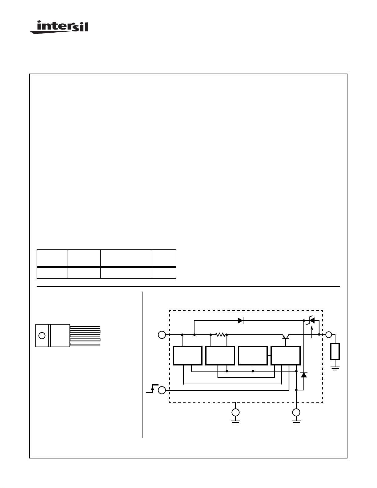
The Functional Block Diagram for the HIP1031 shows the
protection control circuit functions of over-current, overvoltage
and over-temperature. A small metal resistor senses
overcurrent in the power supply path of the pass transistor
and load. Overvoltage detection and shutdown of the output
driver occurs when a comparator determines that the supply
voltage has exceeded a comparator reference level. Overtemperature is sensed from a V
that is thermally close to the output drive transistor. In addition
to the input detected overvoltage protection, negative peak
voltage of an inductive load is clamped with an internal zener
diode. An internal bandgap supply voltage source provides a
stable voltage reference over the chip operating temperature
range, providing bias and reference control for the protection
circuits.
The HIP1031 is particularly well suited for driving lamps,
relays, and solenoids in automotive and industrial control
applications where voltage and current overload protection at
high temperatures is required. The HIP1031 is supplied in a 5
lead TS-001AA Pow er SIP package.
differential sense element
BE
Pinout
HIP1031 (SIP)
TOP VIEW
5 VIN (CONTROL)
4 GND
3 TAB GND
(LOAD)
2 V
OUT
(SUPPLY)
1 V
CC
CAUTION: These devices are sensitive to electrostatic discharge; follow proper IC Handling Procedures.
http://www.intersil.com or 407-727-9207
| Copyright © Intersil Corporation 1999
Functional Block Diagram
V
CC
1
V
BATT
SUPPLY
V
IN
5
CONTROL
OVER-
VOLTAGE
SHUTDOWN
1
R
S
CURRENT
LIMIT
THERMAL
LIMIT
TAB
GND GND
CONTROL
CIRCUIT
43
File Number 3596.6
NEG.
CLAMP
ZENER
HIP1031
V
OUT
2
LOAD

HIP1031
Absolute Maximum Ratings Thermal Information
Supply Voltage, VCC. . . . . . . . . . . See O.V. Shutdown Limit, V
OVSD
Input Voltage, VIN (Note 1). . . . . . . . . . . . . . . . . . . . . . -0.8V to +7V
Load Current, I
Load Dump (Survival) . . . . . . . . . . . . . . . . . . . . . . . . . . ±60V
. . . . . . . . . . . . . . . . . . . . . . . Internally Limiting
OUT
PEAK
Reverse Battery . . . . . . . . . . . . . . . . . . . . . . . . . . . . . . . . . . . . -16V
Operating Conditions
Temperature Range . . . . . . . . . . . . . . . . . . . . . . . . . -40oC to 125oC
CAUTION: Stresses above those listed in “Absolute Maximum Ratings” may cause permanent damage to the device. This is a stress only rating and operation
of the device at these or any other conditions above those indicated in the operational sections of this specification is not implied.
NOTES:
1. The Input Control Voltage, VIN, may range from -0.85V to +7V for a VCC supply voltage of 0V to +25V.
2. θJA is measured with the component mounted on an evaluation PC board in free air.
3. The worst case thermal resistance, θJC for the SIP TS-001AA 5 pin package is 4oC/W. The calculation for dissipation and junction
temperature rise due to dissipation is:
PD = (VCC-V
TJ = T
AMBIENT
Refer to Figure 1 for Derating based on Dissipation and Thermal Resistance. Derating from 150oC is based on the reciprocal of thermal
resistance, θJC+θHS. For example: WhereθJC = 4oC/W and given θHS = 6o/W as the thermal resistance of an external Heat Sink, the
junction-to-air thermal resistance, θJA= 10oC/W. Therefore, for the maximum allowed dissipation, derate 0.1W/oC for each degree from
T
to the maximum rated junction temperature of 150oC. If T
AMB
)(I
OUT
OUT
) + (VCC)(I
CCMAX
- I
OUT
+ (PD) (θJC) for an infinite Heat Sink.
) or (VCC)(I
Thermal Resistance (Typical, Note 2) θJA (oC/W) θJC (oC/W)
Plastic SIP Package . . . . . . . . . . . . . . 50 4
Maximum Power Dissipation, (Note 3)
At TA = 125oC, Infinite Heat Sink. . . . . . . . . . . . . . . . . . . . . 6.25W
Maximum Junction Temperature, TJ. . . . . . . . . . . . . . . . . . . . 150oC
Maximum Storage Temperature Range . . . . . . . . . .-40oC to 150oC
Maximum Lead Temperature (Soldering 10s). . . . . . . . . . . . . 300oC
(Lead Tips Only)
) - (V
CCMAX
= 100oC, the maximum PD is (150 - 100) x 0.1W/oC = 5W.
AMB
OUT
)(I
)
OUT
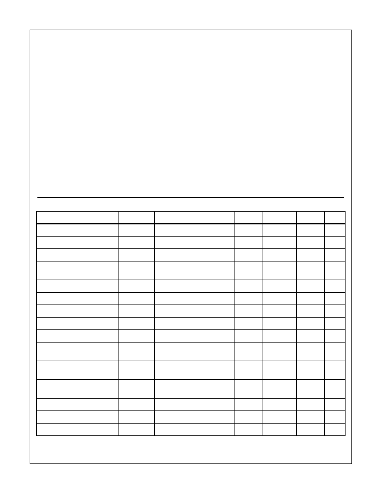
Electrical Specifications T
= -40οC to 125οC, VIN = 2V, VCC = +12V, Unless Otherwise Specified
A
PARAMETER SYMBOL TEST CONDITIONS MIN TYP MAX UNITS
Operating Voltage Range V
Over-Voltage Shutdown V
Over-Temperature Limiting T
Negative Pulse
Output Clamp Voltage
Short Circuit Current Limiting I
Input Control ON V
Input Control OFF V
Input Current High I
Input Current Low I
Supply Current, Full Load,
Input Control ON
Supply Current, No Load,
Input Control OFF
CC
OVSD
SD
V
CL
SC
IH
IL
IH
IL
I
CCMAX
I
CCMIN
4.5 - 25 V
RL = 1kΩ, VIN = 2V 26 33 38 V
o
ICL = -100mA, VCC = 4.5V to 25V,
- 150 -
(VCC - 62) (VCC - 37) (VCC - 28) V
VIN = 0.8V
(Note 4) 0.7 1.1 1.7 A
2.0 - - V
- - 0.8 V
VIN = 5.5V, VCC = 6V to 24 10 - 40 µA
VIN = 0.8V, VCC = 6V to 24V 10 - 30 µA
VIN = 2V; I
VIN = 0V; I
= 0.55A - - 0.6 A
OUT
= 0A - 55 150 µA
OUT
C
Input-Output Forward Voltage
Drop (VCC - V
OUT
)
Output Leakage I
Turn-On Time t
Turn-OFF Time t
V
SAT
OUT_LK
ON
OFF
I
= 0.6A, VCC = 4.5V to 25V - - 1.0 V
OUT
VIN = 0.8V, VCC = 6V to 24V - - 50 µA
RL = 80Ω, TA = 125°C-620µs
RL = 80Ω, TA = 125°C - 17 65 µs
NOTE:
4. Short Circuit current will be reduced when Thermal Shutdown occurs. Testing of a short circuit current may require a short duration pulse.
2
 Loading...