HIP1020
Data Sheet August 1999 File Number 4601.1
Single, Double or Triple-Output Hot Plug
Controller
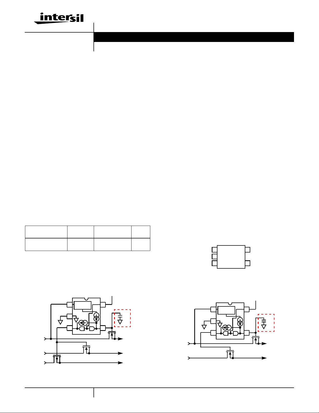
The HIP1020 applies a linear voltage ramp to the gates of
any combination of 3.3V, 5V, and 12V MOSFETs. The
internal charge pump doublesa 12V bias or triples a 5V bias
to deliver the high-side drive capability required when using
more cost-effective N-Channel MOSFETs. The 5V/ms ramp
rate is controlled internally and is the proper value to turn on
most devices within the Device-Bay-specified di/dt limit. If a
slower rate is required, the internally-determined ramp rate
can be over ridden using an optional external capacitor.
When VCC = 12V, the charge pump ramps the voltage on
HGATE from zero to 22V in about 4ms. This allows either a
standard or a logic-levelMOSFET to become fully enhanced
when used as a high-side switch for 12V power control. The
voltage on LGATE ramps from zero to 16V allowing the
simultaneous control of 3.3V and/or 5V MOSFETs.
When VCC = 5V, the charge pump enters voltage-tripler
mode. The voltage on HGATE ramps from zero to 12.5V in
about 3ms while LGATE ramps to 12.0V. This mode is ideal
for control of high-side MOSFET switches used in 3.3V and
5V power switching when 12V bias is not available.
Ordering Information
PART
NUMBER
HIP1020CK-T 0 to 70 5 Ld SOT23 Tape
TEMP.
RANGE (oC) PACKAGE
and Reel
PKG.
NO.
P5.064
Features
• Rise Time Controlled to Device-Bay Specifications
• No Additional Components Required
• Internal Charge Pump Drives N-Channel MOSFETs
• Drives any Combination of One, Two or Three Outputs
• Internally-Controlled Turn-On Ramp
- Optional Capacitor Selects Slower Rates
• Prevents False Turn on During Hot Insertion
• Operates using 12V or 5V Bias
• Improves Device Bay Peripheral Size Cost and Complexity
- Minimal Component Count
- Tiny 5-Pin SOT23 Package
• Controls Standard and Logic-Level MOSFETs
• Compatible with TTL and 3.3V Logic Devices
• Shutdown Current . . . . . . . . . . . . . . . . . . . . . . . . . . < 1µA
• Operating Current. . . . . . . . . . . . . . . . . . . . . . . . . . < 3mA
Applications
• Device Bay Peripherals
• Hot Plug Control
• Power Distribution Control
Pinout
HIP1020 (SOT23)
TOP VIEW
VCC
GND
LGATE
1
2
3
5
4
EN
HGATE
Typical Applications
HIP1020
CHARGE
1
PUMP
2
34
V
12
V
5
V
33
FIGURE 1A. DEVICE-BAY HOT PLUG CONTROLLER WITH
VCC = 12V
2-1
ENABLE
5
OPTIONAL
C1
V
12,OUT
V
5,OUT
V
33,OUT
CAUTION: These devices are sensitive to electrostatic discharge; follow proper IC Handling Procedures.
HIP1020
CHARGE
1
PUMP
2
34
V
5
V
33
FIGURE 1B. DEVICE-BAY HOT PLUG CONTROLLER WITH
VCC = 5V
1-888-INTERSIL or 321-724-7143
| Copyright © Intersil Corporation 1999
ENABLE
5
OPTIONAL
C1
V
V
5,OUT
33,OUT

HIP1020
Pin Descriptions
PIN SYMBOL FUNCTION DESCRIPTION
1 VCC Bias Supply Connect this pin to either a 12V or a 5V source. The HIP1020 detects the bias-voltage level at
pin 1 and decides whether to operate as a voltage-doubler or a voltage-tripler. Consequently,
it is not recommended to operate with bias voltages between 5V (±10%) and 12V (±10%). In
the absence of an enable signal at pin 5, the current into pin 1 is less than 1µA. It is necessary
for voltage to be present at pin 1 prior to applying an enable signal at pin 5.
2 GND Ground Connect to the negative rail of the supply that is connected to pin 1.
3 LGATE Gate Driver for the 5V
and/or 3.3V
MOSFET(s)
4 HGATE 12V or 5V MOSFET
Gate Driver
5 EN Enable Connect a TTL or 3.3V logic signal to this pin to control the outputs at pins 3 and 4. A rising
When VCC = 12V, connect this pin to the gate(s) of the 5V and/or 3.3V MOSFETs. When VCC
= 5V, connect this pin to the gate of a 3.3V MOSFET. Upon a rising edge on EN (pin 5), the
voltage on this pin will ramp linearly to ~16V when VCC = 12V and ~12V when VCC = 5V. An
internal dv/dt activated clamp shunts couplednoise to ground preventing unintended turnon at
either output. The internal dv/dt-activated clamp also protects pin 5.
When VCC = 12V, connect this pin to the gate of the 12V MOSFET. When VCC = 5V, connect
this pin to the gate of the 5V MOSFET. Upon a rising edge on EN (pin 5), the voltage on this
pin will ramp linearly to ~22V when VCC = 12V and ~13V when VCC = 5V.
edge on pin 5 initiates the linear voltage ramps at pins 3 and 4. Be sure that the device driving
EN does not enter a high-impedance state when enabling is not desired and that it’s maximum
rise time does not exceed 100µs.
2-2
 Loading...