Intersil Corporation HIP1016, HIP1015 Datasheet

TM
HIP1015, HIP1016
Data Sheet May 2000
Power Distribution Controllers
The HIP1015 and HIP1016 are hot swap power controllers.
The HIP1015 is targeted for a +12V bus whereas the
HIP1016 is targeted for +5V applications. Each has an
undervoltage (UV) monitoring and reporting with a threshold
level ~17% lower than the nominal +12V and +5V.
The HIP1015 has an integrated charge pump allowing
control of up to a +12V bus using an external N-channel
MOSFET. The HIP1016 can also be used to control much
higher positive or negative voltages in a low side controller
configuration. Both the HIP1015 and HIP1016 feature
programmable Overcurrent (OC) detection, current limiting
regulation with time delay to latch off and soft start.
Ordering Information
TEMP.
PART NUMBER
HIP1015CB 0 to 85 8 Lead SOIC M8.15
HIP1015CB-T 0 to 85 8 Lead SOIC
HIP1016CB 0 to 85 8 Lead SOIC M8.15
HIP1016CB-T 0 to 85 8 Lead SOIC
RANGE (oC) PACKAGE
Tape and Reel
Tape and Reel
PKG.
NO.
M8.15
M8.15
File Number 4778.1
Features
• HOT SWAP Single Power Distribution Control (HIP1015
for 12V, HIP1016 for 5V and Low Side Switch)
• Undervoltage Monitoring and Notification
• Overcurrent Fault Isolation
• Programmable Current Regulation Level
• Programmable Current Limit Time to Latch-Off
• Rail to Rail Common Mode Input Voltage Range
(HIP1015)
• Internal Charge Pump Allows the use of N-channel
MOSFET (HIP1015)
• Undervoltage and Overcurrent Latch Indicators
• Adjustable Turn-On Ramp
• Protection During Turn On
• Two Levels of Overcurrent Detection Provide Fast
Response to Varying Fault Conditions
• Less Than 1µs Response Time to Dead Short
Applications
• Power Distribution Control
• Hot Plug Components and Circuitry
• High Side Low Voltage (< +15V) Switching
• Low Side High Voltage (> +15V, Negative V) Switch
Pinout
HIP1015, HIP1016 (SOIC)
TOP VIEW
ISET
ISEN
GATE
VSS
1
2
3
4
8
7
6
5
PWRON
PGOOD
CTIM
VDD
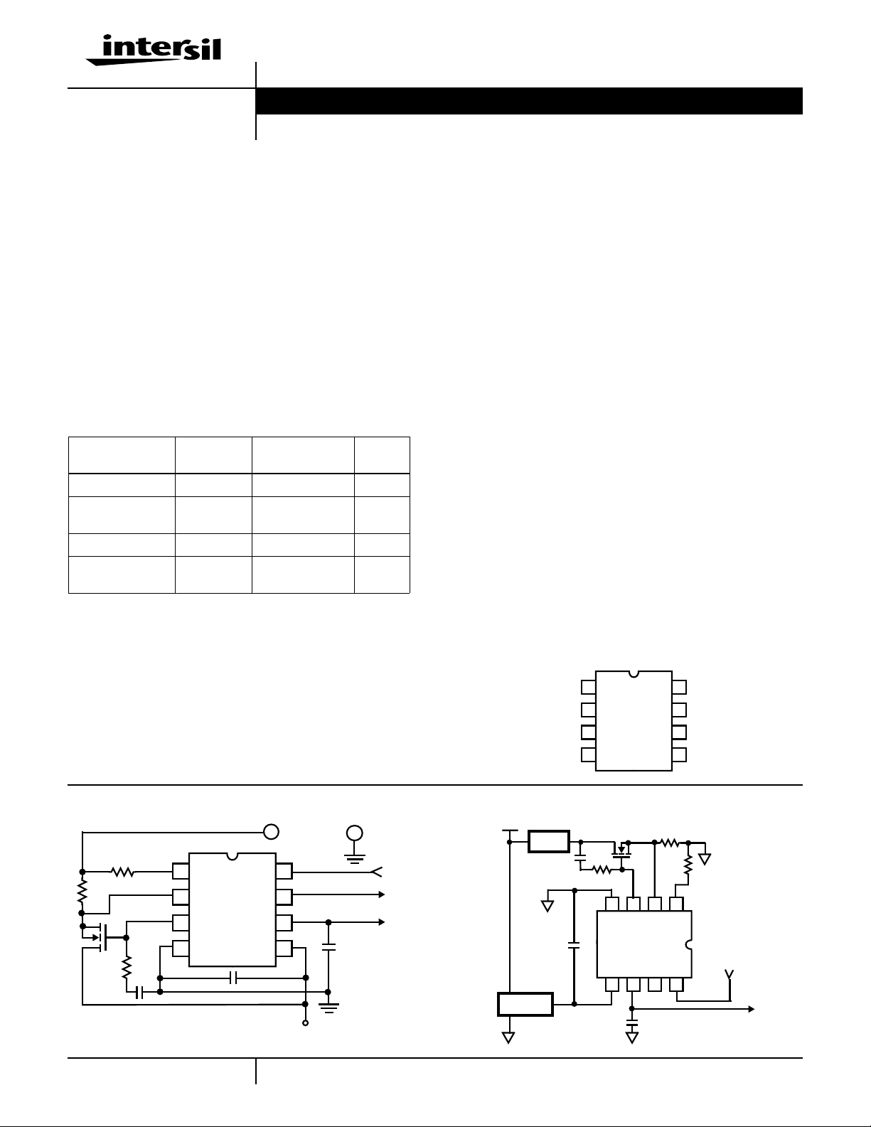
Application One - High Side Controller Application Two - Low Side Controller
+VBUS
12V REG
LOAD
4
5
3
HIP1016
6
1
2
PWRON
8
7
OC
1
2
3
4
HIP1015
+
8
7
6
5
+12V
LOAD
-
PWRON
PGOOD
OC
1
1-888-INTERSIL or 321-724-7143 | Intersil and Design is a trademark of Intersil Corporation. | Copyright © Intersil Corporation 2000
CAUTION: These devices are sensitive to electrostatic discharge; follow proper IC Handling Procedures.

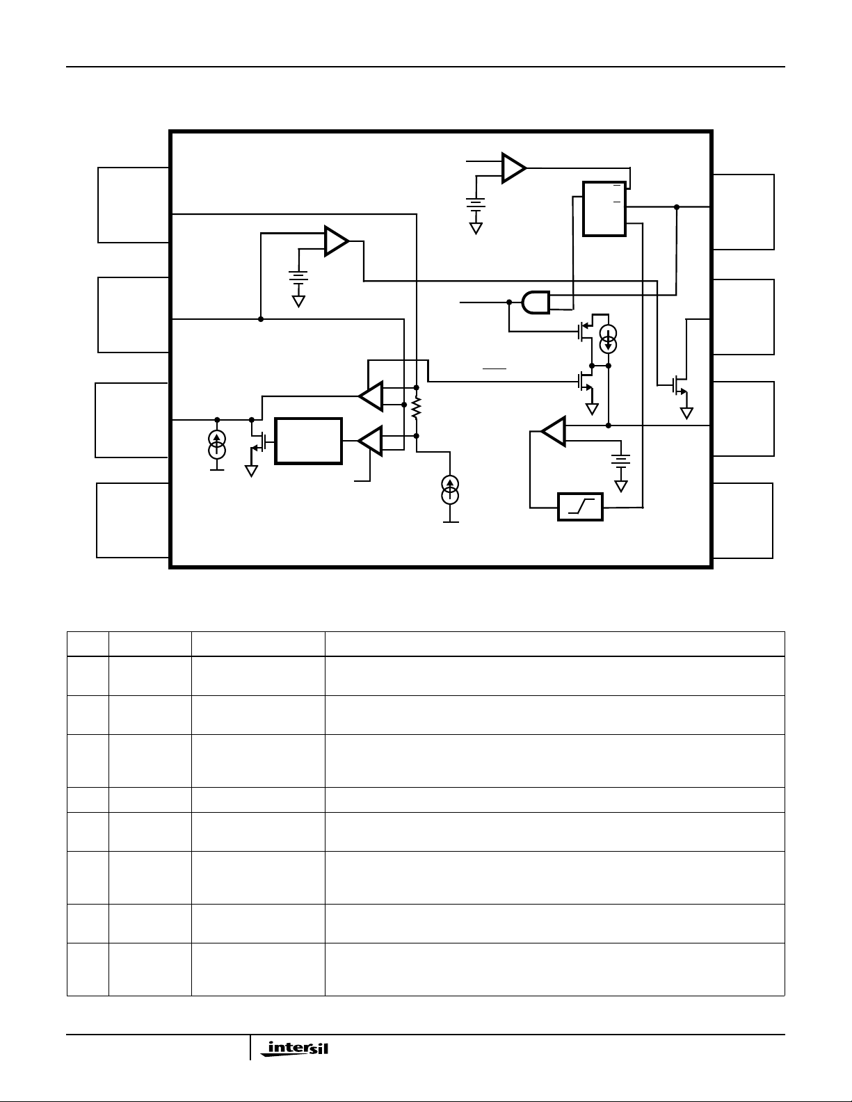
Simplified Block Diagram
I
SET
I
SEN
GATE
10µA
18V
+
-
FALLING
EDGE
DELAY
ENABLE
HIP1015, HIP1016
V
DD
+
-
+
POR
8V
-
-
+
UV
V
REF
ENABLE
20µA
CLIM
+
-
OC
+
-
-
+
WOCLIM
7.5k
QN
Q
12V
1.86V
R
R
S
10µA
PWRON
PGOOD
CTIM
+
-
V
SS
18V
RISING
EDGE
PULSE
V
Pin Descriptions
PIN # SYMBOL FUNCTION DESCRIPTION
1 ISET Current Set Connect to thelow side of the current sense resistor through the current limiting set resistor.
This pin functions as the current limit programming pin.
2 ISEN Current Sense Connect to the more positive end of sense resistor to measure the voltage drop across this
resistor
3 GATE External FET Gate Drive
Pin
4 VSS Chip Return
5VDDChip Supply 12V chip supply. Thiscan be eitherconnected directly tothe +12V rail supplying the switched
6 CTIM Current Limit Timing
Capacitor
7 PGOOD Power Good Indicator Indicates that the voltage on ISEN pin is within specification. PGOOD is driven by an open
Connectto the gate of theexternalN-Channel MOSFET. A capacitor fromthisnode to ground
sets the turn-on ramp. At turn-on this capacitor will be charged to VDD+5V (HIP1015) and to
VDD(HIP1016) by a 10µA current source.
load voltage or to a dedicated VSS +12V supply.
Connect a capacitor from this pin to ground. This capacitor determines the time delay
between an overcurrent eventand chip outputshutdown (current limittime-out). The duration
of current limit time-out (in seconds) = 93kΩ x C
TIM
(Farads).
drain N-Channel MOSFET and is pulled low when the output is not within specification.
DD
8 PWRON Power ON PWRONis used to controland reset the chip.The chip is enabledwhen PWRON pin isdriven
high or is open. After a current limit time out, the chip is reset by a low level signal applied to
this pin. This input has 20µA pull up capability
2

HIP1015, HIP1016
Absolute Maximum Ratings T
VDD . . . . . . . . . . . . . . . . . . . . . . . . . . . . . . . . . . . . . . .-0.3V to +16V
GATE . . . . . . . . . . . . . . . . . . . . . . . . . . . . . . . . . . . -0.3V to VDD+8V
ISEN, PGOOD, PWRON, CTIM, ISET. . . . . . . .-0.3V to VDD+ 0.3V
ESD Classification . . . . . . . . . . . . . . . . . . . . . . . . . . . . . . . . . . . .5kV
= 25oC Thermal Information
A
Thermal Resistance (Typical, Note 1) θJA (oC/W)
SOIC Package . . . . . . . . . . . . . . . . . . . . . . . . . . . . . 98
Maximum Junction Temperature (Plastic Package) . . . . . . . .150oC
Maximum Storage Temperature Range. . . . . . . . . . -65oC to 150oC
Maximum Lead Temperature (Soldering 10s) . . . . . . . . . . . . .300oC
Operating Conditions
(SOIC - Lead Tips Only)
VDD Supply Voltage Range. . . . . . . . . . . . . . . . . . . . . . +12v+/-15%
Temperature Range (TA) . . . . . . . . . . . . . . . . . . . . . . . .0oC to 85oC
CAUTION: Stresses above those listed in “Absolute Maximum Ratings” may cause permanent damage to the device. This is a stress only rating and operation of the
device at these or any other conditions above those indicated in the operational sections of this specification is not implied.
NOTES:
1. θJAismeasured with the component mounted onahigh effectivethermal conductivity test board infreeair.(See TechBrief, #TB379.1 fordetails.)
2. All voltages are relative to GND, unless otherwise specified.
Electrical Specifications V
= 12V, TA = TJ = 0oC to 85oC, Unless Otherwise Specified
DD
PARAMETER SYMBOL TEST CONDITIONS MIN TYP MAX UNITS
ISET Current Source I
ISET
Current Limit Amp Offset Voltage V
Current Limit Time-Out Threshold Voltage C
GATE Response Time To Severe
_Vth CTIM Voltage 1.3 1.8 2.3 V
TIM
pd_woc_amp V
- V
ISET
ISEN
to 10.8V - 100 - ns
GATE
18.5 20 21.5 µA
-6 0 6 mV
Overcurrent
GATE Response Time to Overcurrent pd_oc_amp V
GATE Turn-On Current I
GATE
to 10.8V 600 ns
GATE
V
to = 6V 8.4 10 11.6 µA
GATE
GATE Pull down Current OC_GATE_I_4V Overcurrent 45 75 mA
GATE Pull down Current WOC_GATE_I_4V Severe Overcurrent 0.5 0.8 1.5 A
HIP1015 Undervoltage Threshold 12V
HIP1015 Undervoltage Disabled 12V
UV_VTH
UV_VTH_dis
9.2 9.6 10 V
VDD+1.9V VDD+2.5V V
HIP1015 GATE High Voltage 12VG GATE Voltage VDD+4.5V VDD+5V - V
HIP1016 Undervoltage Threshold 5V
HIP1016 Undervoltage Disabled 5V
UV_VTH
UV_VTH_dis
HIP1016 GATE High Voltage 5VG GATE Voltage VDD-1.5V V
VDD Supply Current I
VDD POR Rising Threshold V
VDD POR Falling Threshold V
VDD POR Threshold Hysteresis V
VDD
DD_POR_L2H
DD_POR_H2L
DD_POR_HYS
VDD Low to High 7.8 8.4 9 V
VDD High to Low 7.5 8.1 8.7 V
V
DD_POR_L2H -VDD_POR_H2L
4.0 4.35 4.5 V
VDD-3V VDD-2.5V V
DD
-V
-35mA
0.1 0.3 0.6 V
PWRON Pull-up Voltage PWRN_V PWRON Pin Open 2.7 3.2 - V
PWRON Rising Threshold PWR_Vth 1.4 1.7 2.0 V
PWRON Hysteresis PWR_hys 130 170 250 mV
PWRON Pull-Up Current PWRN_I 9 17 25 µA
C
Charging Current C
TIM
C
Fault pull-up Current 16 20 23 mA
TIM
_ichg0 V
TIM
= 0V 16 20 23 µA
CTIM
HIP1015 ISEN Current ISEN_5V_I 41 72 88 µA
HIP1016 ISEN Current ISEN_5V_I 100 145 170 µA
3
 Loading...