

2-406
HIP1013
Low Cost Dual Power Distribution
Controller
The HIP1013 is a low cost HOT SWAP dual supply power
distribution controller. Two external N-Channel MOSFETs
are driven to distribute power while providing load fault
isolation. At turn-on, the gate of each external N-Channel
MOSFET is charged with a 10µA current source. Capacitors
on each gate (see theTypical Application Diagram),createa
programmable ramp(soft turn-on) to control inrush currents.
A built in charge pump supplies the gate drive for the 12V
supply N-Channel MOSFET switch.
Over current protection is facilitated by two external current
sense resistors. When the current through either resistor
exceeds the user programmed value the N-Channel
MOSFETs are latched off by the HIP1013. The controller is
reset by a rising edge on either
PWRON pin.
Choosing the voltage selection mode the HIP1013 controls
either +12V/5V or +3.3V/+5V supplies.
Although pin compatible with the HIP1012 device, the
HIP1013 does not offer current regulation during an
OC event.
Features
• HOT SWAP Dual Power Distribution Control for +5V and
+12V or +5V and +3.3V
• Provides Fault Isolation
• Charge Pump Allows the Use of N-Channel MOSFETs
• Redundant Power On Controls
• Power Good and Over Current Latch Indicators
• Adjustable Turn-On Ramp
• Protection During Turn-On
Applications
• Power Distribution Control
• Hot Plug™ Components
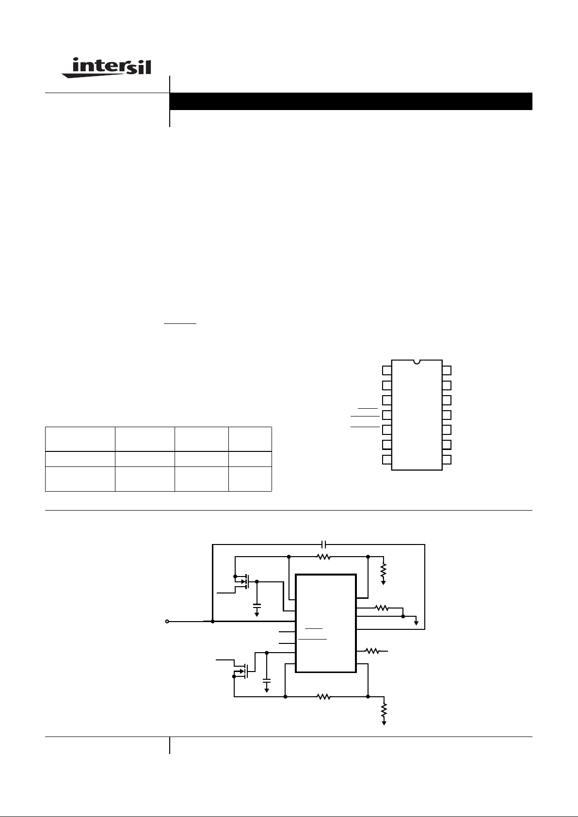
Pinout
HIP1013 (SOIC)
TOP VIEW
Typical Application Diagram
Ordering Information
PART
NUMBER
TEMP. RANGE
(oC) PACKAGE PKG. NO.
HIP1013CB -0 to 70 14 Ld SOIC M14.15
HIP1013CB-T -0 to 70 14 Ld SOIC
Tape and Reel
M14.15
3/12VS
3/12VG
V
DD
PWRON2
5VG
5VS
3/12VISEN
GND
C
PUMP
NC
R
ILIM
PGOOD
5VISEN
MODE/
PWRON1
1
2
3
4
5
6
7
14
13
12
11
10
9
8
3/12VS
3/12VG
PWRON2
PGOOD
5VG
5VS
3/12VISEN
GND
NC
R
ILIM
C
PUMP
5ISEN
V
DD
HIP1013
12V
R
LOAD
R
ILIM
C
PUMP
R
SENSE
5V
R
LOAD
R
SENSE
5V
V
DD
C
GATE
C
GATE
M/PON1
POWER ON
INPUTS
Data Sheet May 1999 File Number
4516.2
CAUTION: These devices are sensitive to electrostatic discharge; follow proper IC Handling Procedures.
Hot Plug™ is a trademark of Core International, Inc.
http://www.intersil.com or 407-727-9207
| Copyright © Intersil Corporation 1999
2-407
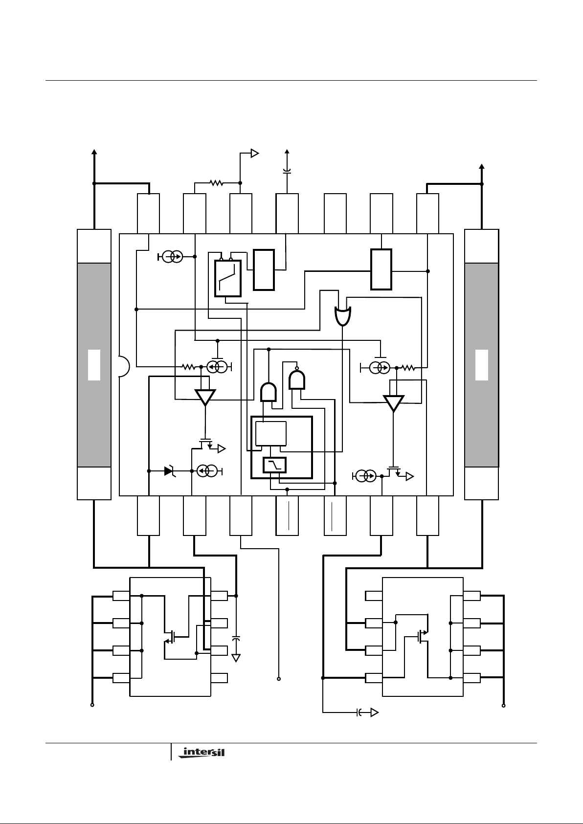
Functional Diagram
V
DD
12VG
12VS
12ISEN
5VG
5VS
5ISEN
GND
MODE/
PGOOD
R
ILIM
C
PUMP
PWRON2
QPUMP
100µA
RISING
V
DD
RRS
QN
Q
POR
10µA
EDGE
RESET
C
PUMP
R
ILIM
12V
TO LOAD
TO LOAD
12VIN
5VIN
HIP1013
C
GATE
C
GATE
TO V
DD
+
-
R
SENSE
PGOOD
ENABLE
10µA
18V
+
-
12V
R
SENSE
NC
PWRON1
OC
OC
12V
18V
HIP1013
2-408
Pin Description
PIN NO. SYMBOL FUNCTION DESCRIPTION
1 12VS 12V Source Connect to source of associated external N-Channel MOSFET switch to sense output
voltage.
2 12VG 12V Gate Connect to the gate of associated N-Channel MOSFET switch. A capacitor from this
node toground setsthe turn-onramp. At turn-on this capacitor will be charged to ≈17.4V
bya10µA current source when in 5V/12V mode of operation, otherwise capacitor will be
charged to ≈11.4V.
3VDDChip Supply Connect to 12V supply. This can be either connected directly to the +12V rail supplying
the load voltage or to a dedicated VDD +12V supply.
4 MODE/
PWRON1
Power ON/ Reset invokes
3.3V operation when
shorted to VDD, Pin 3.
PWRON1 and PWRON2 are used to turn-on and reset the chip. Both outputs turn-on
wheneitherpin is driven low. After an over current limit fault, the chip is reset by the rising
edge of a reset signal applied to either PWRON pin. Each input has 100µA pull up
capability which is compatible with 3V and 5V open drain and standard logic. PWRON1
is also used to invoke 3.3V control operation in preference to +12V control. By tying pin
4 to pin 3 the charge pump is disabled and the UV threshold also shifts to ≈2.8V.
5 PWRON2 Power ON/Reset
6 5VG 5V Gate Connect to the gate of the external 5V N-Channel MOSFET. A capacitor from this node
to ground sets the turn-on ramp. At turn-on this capacitor will be charged to ≈11.4V by a
10µA current source.
7 5VS 5V Source Connect to the source side of 5V external N-Channel MOSFET switch to sense output
voltage.
8 5VISEN 5V Current Sense Connect to the load side of the 5V sense resistor to measure the voltage drop across this
resistor between 5VS and 5VISEN pins.
9 PGOOD Power Good Indicator PGOOD is driven by an open drain N-Channel MOSFET. It is pulled low when either
output voltage is not within specification or and OC condition exists.
10 No Connection.
11 C
PUMP
Charge Pump Capacitor Connect a 0.1µF capacitor between this pin and VDD (Pin 3).
12 GND Chip Ground
13 R
ILIM
Current Limit Set Resistor A resistor connected between this pin and ground determines the current level at which
current limit is activated. This current is determined by the ratio of the R
ILIM
resistor to
the sense resistor (R
SENSE
). The current at current limit onset is equal to
10µAx(R
ILIM/RSENSE
).
14 12VISEN 12V Current Sense Connect to the load side of sense resistor to measure the voltage drop across this
resistor.
HIP1013

2-409
Absolute Maximum Ratings T
A
=25oC Thermal Information
VDD . . . . . . . . . . . . . . . . . . . . . . . . . . . . . . . . . . . . . -0.3V to +13.2V
3/12VG, C
PUMP
. . . . . . . . . . . . . . . . . . . . . . . . . . . . . -0.3V to 18.5V
3/12VISEN, 3/12VS . . . . . . . . . . . . . . . . . . . . . . . -5V to VDD+ 0.3V
5VISEN, 5VS . . . . . . . . . . . . . . . . . . . . . . . . . . . . . . . . . .-5V to 7.5V
PGOOD, R
ILIM
. . . . . . . . . . . . . . . . . . . . . . . . . . . . . . . -0.3V to 7.5V
MODE/PWRON1, PWRON2, 5VG . . . . . . . . . .-0.3V to VDD + 0.3V
ESD Classification . . . . . . . . . . . . . . . . . . . . . . . . . . . . 2kV (Class 2)
Operating Conditions
VDD Supply Voltage Range. . . . . . . . . . . . . . . . . .+10.5V to +13.2V
Temperature Range (TA) . . . . . . . . . . . . . . . . . . . . . . . .0oC to 70oC
Thermal Resistance (Typical, Note 1) θJA (oC/W)
SOIC Package . . . . . . . . . . . . . . . . . . . . . . . . . . . . . 120
Maximum Junction Temperature (Plastic Package) . . . . . . . .150oC
Maximum Storage Temperature Range. . . . . . . . . . -65oC to 150oC
Maximum Lead Temperature (Soldering 10s) . . . . . . . . . . . . .300oC
(SOIC - Lead Tips Only)
CAUTION: Stresses above those listed in “Absolute Maximum Ratings” may cause permanent damage to the device. This is a stress only rating and operationofthe
device at these or any other conditions above those indicated in the operational sections of this specification is not implied.
NOTES:
1. θJA is measured with the component mounted on an evaluation PC board in free air.
2. All voltages are relative to GND, unless otherwise specified.
Electrical Specifications V
DD
= 12V, CVG = 0.01µF, R
SENSE
= 0.1Ω, C
BULK
= 220µF, ESR = 0.5Ω, TA = TJ = 0oC to 70oC, Unless
Otherwise Specified
PARAMETER SYMBOL TEST CONDITIONS MIN TYP MAX UNITS
CONTROL SECTION
Current Limit Threshold Voltage
(Voltage Across Sense Resistor)
V
IL
R
ILIM
= 10kΩ 85 100 115 mV
Over Current Limit Response Time OC
Lrt
Current Overload, R
ILIM
= 10kΩ, R
SHORT
= 6.0Ω -2-µs
Response Time To Dead Short RT
SHORTCVG
= 0.01µF - 500 1000 ns
12V Gate Turn-On Time t
ON12VCVG
= 0.01µF - 12 - ms
5V Gate Turn-On Time t
ON5V
CVG= 0.01µF-5-ms
Gate Turn-On Current I
ON
CVG= 0.01µF 8 10 12 µA
12V Under Voltage Threshold 12V
VUV
10.5 10.8 11.0 V
5V Under Voltage Threshold 5V
VUV
4.35 4.5 4.65 V
3.3V Under Voltage Threshold 3.3V
VUV
2.65 2.8 2.95 V
Charge pumped 12VG Voltage V12VG C
PUMP
= 0.1µF 16.8 17.3 17.9 V
3/5VG High Voltage 3/5VG 11.2 11.9 - V
SUPPLY CURRENT AND IO SPECIFICATIONS
V
DD
Supply Current I
VDD
4 8 10 mA
V
DD
POR Rising Threshold POR
rvth
9.5 10.0 10.5 V
V
DD
POR Falling Threshold POR
fvth
9.3 9.8 10.3 V
PWRON Pull-up Voltage PWRN_V PWRON pins open 1.8 2.4 3.2 V
PWRON Rising Threshold PWR_Vth 1.1 1.5 2 V
PWRON Hysteresis PWR_hys 0.1 0.2 0.3 V
PWRON Pull-Up Current PWRN_I 60 80 100 µA
R
ILIM
Pin Current Source Output R
ILIM
_Io 90 100 110 µA
Charge Pump Output Current Qpmp_Io C
PUMP
= 0.1µF, C
PUMP
= 16V 400 590 800 µA
Charge Pump Output Voltage Qpmp_Vo No load 17.2 17.4 - V
Charge Pump Output Voltage - Loaded Qpmp_VIo Load current = 100µA 16.2 16.7 - V
Charge Pump POR Rising Threshold Qpmp+Vth 15.6 16 16.5 V
Charge Pump POR Falling Threshold Qpmp-Vth 15.2 15.7 16.2 V
HIP1013

2-410
Typical Performance Curves
FIGURE 1. SUPPLY CURRENT FIGURE 2. R
ILIM
SOURCE CURRENT
FIGURE 3. 12V UV THRESHOLD FIGURE 4. 3.3V/5V UV THRESHOLD
FIGURE 5. 12V, 5V GATE DRIVE FIGURE 6. CHARGE PUMP VOLTAGE
8.2
8.0
7.8
7.6
7.4
7.2
-40 -20 0 20 40 60 80
TEMPERATURE (
o
C)
8.4
SUPPLY CURRENT(mA)
-30 -10 10 30 50 70
104
103
-40 -20 0 20 40 60 80
102
70503010-10-30
105
TEMPERATURE (
o
C)
CURRENT (µA)
TEMPERATURE (oC)
12V UV THRESHOLD (V)
20 40 60 80-40 -20 0
11.00
10.98
10.96
10.94
3.3V UV
20 40 60 80-40 -20 0
4.615
4.610
4.605
4.600
4.595
2.888
2.886
2.884
2.882
2.880
TEMPERATURE (
o
C)
5V UV THRESHOLD (V)
3.3V UV THRESHOLD (V)
5V UV
12V VG
5V VG
20 40 60 80-40 0-20
17.36
17.34
17.32
17.30
17.28
17.26
11.935
11.930
11.925
11.920
11.915
11.910
11.905
11.900
TEMPERATURE (
o
C)
3.3V, 5V GATE DRIVE (V)
12V GATE DRIVE (V)
20 40 60 80-40 0-20
VOLTAGE (V)
TEMPERATURE (oC)
17.6
17.4
17.2
16.8
16.6
17.0
CHARGE PUMP VOLTAGE
NO LOAD
CHARGE PUMP VOLTAGE
100µA LOAD
HIP1013

2-411
HIP1013 Description and Operation
The HIP1013 offers the designer a cost efficient 5V and 12V
true hot plug controller. This device drives two external
N-Channel MOSFET switches and uses a charge pump to
provide
≈17V to drive the gate of the 12V supply switch. The
HIP1013 features Over Current (OC) programing with a
single external resistor, R
ILIM
and during turn-on, the gate
capacitor of each external N-Channel MOSFET is charged
with a 10µA current source. These capacitors create a
programmable ramp (soft turn-on).
Upon initial power up, the HIP1013 can either isolate the
voltage supply from the load by holding the external
N-Channel MOSFET switches off or apply the supply rail
voltage directly to the load for true hot swap capability. In
either case the HIP1013 turns on in a soft start mode
protecting the supply rail from sudden current loading.
The load currents pass through two external current sense
resistors. When the voltage across either resistor exceeds
the user programmed Over Current (OC) voltage threshold
value, (see Table 1) the HIP1013 controller turns both
N-Channel MOSFETs off in
≈ 2µs.
The HIP1013 is reset by a rising edge on either
PWRON pin
and is turned on by either
PWRON pin being driven low.The
HIP1013 can control either +12V/5V or +3.3V/+5V supplies.
Tying the
PWRON1 pin to VDD, invokes the +3.3V/+5V
voltage mode. In this mode, the external charge pump
capacitor is not needed and C
PUMP
, pin 11 is also tied
directly to V
DD
. Upon any OC or Under Voltage (UV)
condition the PGOOD fault indicating signal will pull low
when tied high through a resistor to the logic supply.
HIP1013 Application Considerations
There is no unique and specific HIP1013 application
evaluation board. Since the HIP1013 is pin compatible with
the HIP1012 device, you can substitute a HIP1013 for the
existing HIP1012 in either of the HIP1012EVAl1 or EVAL2
boards. Otherwise contact your Intersil Corporation sales
office and an already modified board will be provided.
Although pin compatible to the HIP1012, the HIP1013 is a
less featured dual power supply distribution controller and
does not include programmable current limiting regulation
and delay time to latch off.
Random resets can also occur if the HIP1013 (PINS 8 and
14) sense pins are pulled below ground when turning off a
highly inductive load. Place a large load capacitor (10-50µF)
on the output to eliminate unintended resets.
Physical layout of R
SENSE
resistors is critical to avoid
the possibility of false over current occurrences. Ideally
trace routing between the R
SENSE
resistors and the HIP1013
VS and VISEN pins are direct and as short as possible with
zero current in the sense lines.
FIGURE 7. OC VOLTAGE THRESHOLD WITH = R
ILIM
10kΩ FIGURE 8. POWER ON RESET VOLTAGE THRESHOLD
Typical Performance Curves
(Continued)
20 40 60 80-40 0-20
VOLTAGE THRESHOLD (mV)
12 OC VTth
5 OC Vth
TEMPERATURE (
o
C)
102.5
102.0
101.5
101.0
100.5
-40 -20 0 20 40 60 80-30 -10 10 30 50 70
10.2
10.0
9.8
9.6
POWER ON RESET (V)
TEMPERATURE (oC)
VDD LOW TO HIGH
VDD HIGH TO LOW
TABLE 1.
R
ILIM
RESISTOR NOMINAL OC VTH
15K 150mv
10K 100mV
7.5K 75mV
4.99K 50mV
NOTE: Nominal OC Vth = R
ILIM
x 10 µA
CORRECT INCORRECT
TO HIP1013
VS AND VISEN
TO HIP1013
VS AND VISEN
CURRENT
SENSE RESISTOR
HIP1013

2-412
All Intersil semiconductor products are manufactured, assembled and tested under ISO9000 quality systems certification.
Intersil semiconductor products are sold by description only. Intersil Corporation reserves the right to make changes in circuit design and/or specifications at any time without notice. Accordingly, the reader is cautioned to verify that data sheets are current before placing orders. Information furnished by Intersil is believed to be accurate and
reliable. However ,no responsibility is assumed by Intersil or its subsidiaries for its use; nor for any infringements of patents or other rights of third parties which may result
from its use. No license is granted by implication or otherwise under any patent or patent rights of Intersil or its subsidiaries.
For information regarding Intersil Corporation and its products, see web site http://www.intersil.com
Sales Office Headquarters
NORTH AMERICA
Intersil Corporation
P. O. Box 883, Mail Stop 53-204
Melbourne, FL 32902
TEL: (407) 724-7000
FAX: (407) 724-7240
EUROPE
Intersil SA
Mercure Center
100, Rue de la Fusee
1130 Brussels, Belgium
TEL: (32) 2.724.2111
FAX: (32) 2.724.22.05
ASIA
Intersil (Taiwan) Ltd.
7F-6, No. 101 Fu Hsing North Road
Taipei, Taiwan
Republic of China
TEL: (886) 2 2716 9310
FAX: (886) 2 2715 3029
HIP1013
 Loading...