Intersil Corporation HIP1011D Datasheet

HIP1011D
Data Sheet November 1999
Dual PCI Hot Plug Controller
The HIP1011D is the first IC available for independent
control of two PCI Hot Plug slots. The HIP1011D has all the
features and functionality of two single PCI Hot Plug slot
controllers such as the HIP1011A but in the same foot print
area.
The HIP1011D is designed to be physically placed in close
proximity to two adjacent PCI slots servicing each
independently but reducing layoutcomplexityandplacement
costs in assembly. It creates two independent power control
solutions with discrete power MOSFETs and a few passive
components. The four supplies +5V, +3.3V, +12V, and -12V
for each slot are independently controlled. There are four
integrated current sensing switches for the +12V and -12V
and for the +5V and +3.3V supplies overcurrent protection is
provided by sensing the voltage across external currentsense resistors. In addition, on-chip references are used to
monitor the +5V, +3.3V and +12V outputs for undervoltage
conditions. The two PWRON inputs control the state of the
switches, one each for slot A and slot B outputs. During an
overcurrent condition on any output, or an undervoltage
condition on the +5V, +3.3V or +12V outputs, a LOW (0V) is
asserted on the associated FLTN output and all associated
switches are latched-off. The outputs servicing the adjacent
slot are unaffected.
File Number 4725.1
Features
• Independent Power Control of 2 PCI Slots
• Turn-Off Delay Time Adjustability
• Internal MOSFET Switches for +12V and -12V Outputs
• µP Interface for On/Off Control and Fault Reporting
• Adjustable Overcurrent Protection for All Eight Supplies
• Provides Fault Isolation
• Adjustable Turn-On Slew Rate
• Minimum Parts Count Solution
• No Charge Pump
• 100ns Response Time to Over Current
Applications
• PCI Hot-Plug
Ordering Information
TEMP.RANGE
PART NUMBER
HIP1011DCA 0 to 70 28 Ld SSOP M28.15
HIP1011DCA-T 0 to 70 Tape and Reel
(oC) PACKAGE
PKG.
NO.
The time to FLTN signal going LOW and MOSFET latch off
is user determined by a single capacitor from each FLTN pin
to ground. This added feature enables the HIP1011D to
ignore system noise transients. The FLTN latch is cleared
when the PWRON input is toggled low again. During initial
power-up of the main VCC supply (+12V), the PWRON input
is inhibited from turning on the switches,andthelatchisheld
in the Reset state until the VCC input is greater than 10V.
User programmability of the overcurrent threshold and turnon slew rate is provided. A resistor connected to the OCSET
pin programs the overcurrent threshold for both slots.
Capacitors connected to the gate pins set the turn-on rate.
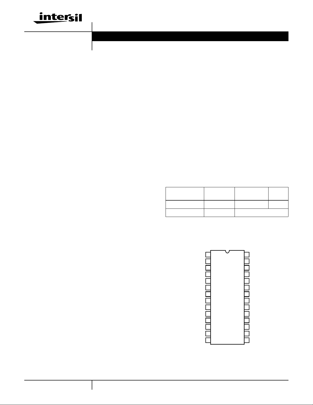
Pinout
M12VO_2
M12VG_2
PWRON_2
VSS
12VG_2
12VO_2
12VO_1
12VG_1
OCSET
FLTN_1
PWRON_1
M12VG_1
M12VO_1
1
2
3
4
5
6
7
8
9
10
11
12
13
14
HIP1011D
(SSOP)
TOP VIEW
28
27
26
25
24
23
22
21
20
19
18
17
16
15
M12VIN_2
3VISEN_2
3VS_2
5VISEN_2FLTN_2
5VS_2
3V5VG_2
12VIN_2
12VIN_1
3V5VG_1
5VS_1
5VISEN_1
3VS_1
3VISEN_1
M12VIN_1
1
CAUTION: These devices are sensitive to electrostatic discharge; follow proper IC Handling Procedures.
1-888-INTERSIL or 321-724-7143
| Copyright © Intersil Corporation 1999

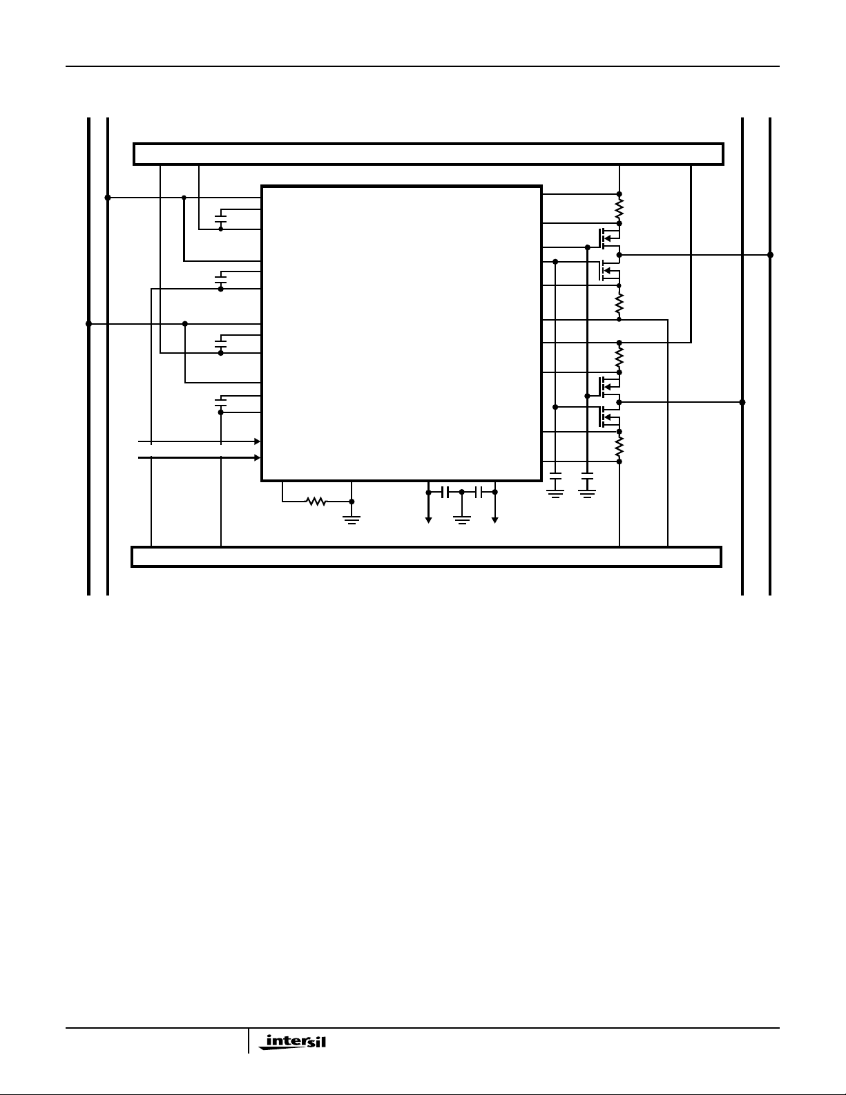
Typical Application
HIP1011D
-12V BUS
+12V BUS
SYSTEM CONTROLLER
-12V12V 3.3V5V
M12VIN_1
M12G_1
C1
M12VO_1
M12VIN_2
M12G_2
C2
M12VO_2
12VIN_1
12VG_1
C3
12VO_1
12VIN_2
12VG_2
C4
12VO_2
FROM
PWRON_1
PWRON_2
OCSET
R5
SLOT 1
HIP1011D
FLTN_1VSS
OPT. OPT.
TO SYSTEM CONTROLLER
SLOT 2
5VISEN_1
3V5VG_1
3V5VG_2
5VISEN_2
3VISEN_1
3VISEN_2
FLTN_2
5VS_1
5VS_2
3VS_1
3VS_2
C5 C6
Q1
Q2
Q3
Q4
R1
R2
R3
R4
5V BUS
3.3V BUS
5V3.3V12V-12V
FIGURE 1.
2

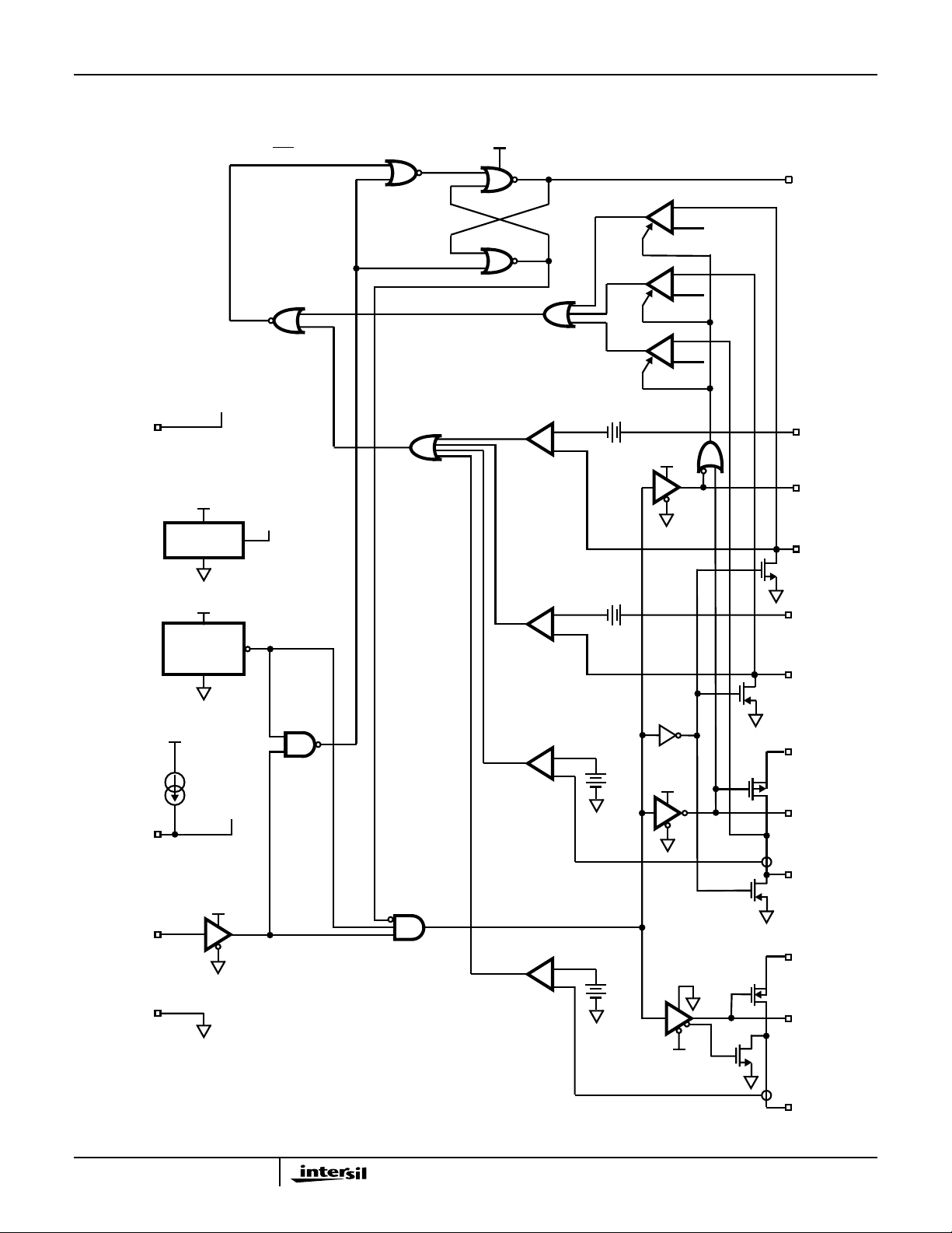
Simplified Schematic (1/2 HIP1011D)
SET (LOW = FAULT)
12VIN
12VIN
HIP1011D
RESET
5VREF
COMP
FAULT LATCH
+
-
LOW = FAULT
COMP
COMP
COMP
-
+
+
INHIBIT
-
+
INHIBIT
-
+
INHIBIT
12VIN
FLTN
4.6V
2.9V
10.6V
5VS
100µA
OCSET
PWRON
GND
12VIN
5V ZENER
REFERENCE
12VIN
12VIN
POWER-ON
RESET
12VIN
V
OCSET
12VIN
5VREF
LOW WHEN
12VIN < 10V
HIGH = FAULT
COMP
+
-
COMP
-
+
HIGH = SWITCHES ON
COMP
-
+
3V5VG
5VISEN
-
+
+
-
+
-
12VIN
0.3Ω
0.7Ω
3VS
3VISEN
12VIN
12VG
12VO
M12VIN
M12VG
M12VIN
FIGURE 2.
M12VO
3

HIP1011D
Pin Descriptions
PIN NO. DESIGNATOR FUNCTION DESCRIPTION
15, 28 M12VIN -12V Input -12V Supply Input. Also provides power to the -12V overcurrent circuitry.
4, 11 FLTN Fault Output 5V CMOS Fault Output; LOW=FAULT. An optional capacitor may be place from this pin to
ground to provide additional immunity from power supply glitches.
20, 23 3V5VG 3.3V/5V Gate Output Drive the gates of the 3.3V and 5V MOSFETs. Connect a capacitor to ground to set the
start-up ramp. During turn on, this capacitor is charged with a 25µA current source.
UV comparator disabled when this pin below 9.6V nominal.
21, 22 12VIN 12V Input 12V supply input for IC and 12VO. Both 12VIns to be connected to a single +12V supply.
16, 27 3VISEN 3.3V Current Sense Connect to the load side of the currentsenseresistorinserieswithsourceofexternal 3.3V
MOSFET.
17, 26 3VS 3.3V Source Connect to source of 3.3V MOSFET. This connection along with (3VISEN) senses the
voltage drop across the sense resistor.
19, 24 5VS 5V Source Connect to source of 5V MOSFET switch. This connection along with (5VISEN) senses the
voltage drop across the sense resistor.
18, 25 5VISEN 5V Current Sense Connect to the load side of the current sense resistor in series with source of external 5V
MOSFET.
3, 12 PWRON Power On Control Controls all four switches. High to turn switches ON, Low to turn them OFF.
6, 9 12VG Gate of Internal PMOS Connect a capacitor between 12VG and 12VO to set the start-up ramp for the +12V supply.
This capacitor is charged with a 25µA current source during start-up.
UV comparator disabled when this pin >1.4Vnominal.
7, 8 12VO Switched 12V Output Switched 12V output. Rated for 0.5A.
2, 13 M12VG Gate of Internal NMOS Connect a capacitor between M12VG and M12VO to set the start-up ramp for the M12V
supply. This capacitor is charged with 25µA during start-up.
1, 14 M12VO Switched -12V
Output
10 OCSET Overcurrent Set Connect a resistor from this pin to ground to set the overcurrent trip point of all eight
5 VSS Ground Connect to common of power supplies.
Switched 12V Output. Rated for 100mA.
switches. All eight over current trips can be programmed by changing the value of this
resistor. The default (6.04kΩ, 1%) is compatible with the maximum allowable currents as
outlined in the PCI specification.
4

HIP1011D
Absolute Maximum Ratings Thermal Information
12VIN. . . . . . . . . . . . . . . . . . . . . . . . . . . . . . . . . . . . -0.5V to +14.0V
12VO, 12VG, 3V5VG . . . . . . . . . . . . . . . . . . . .-0.5V to 12VIN +0.5V
M12VIN . . . . . . . . . . . . . . . . . . . . . . . . . . . . . . . . . . -14.0V to +0.5V
M12VO, M12VG. . . . . . . . . . . . . . . . . . . . . . V
M12VIN
-0.5V to +0.5V
3VISEN, 5VISEN . . . . . . . . . .-0.5V to the Lesser of 12VIN or +7.0V
Voltage, Any Other Pin. . . . . . . . . . . . . . . . . . . . . . . . -0.5V to +7.0V
12VO Output Current. . . . . . . . . . . . . . . . . . . . . . . . . . . . . . . . . . .3A
M12VO Output Current . . . . . . . . . . . . . . . . . . . . . . . . . . . . . . . 0.8A
ESD Classification . . . . . . . . . . . . . . . . . . . . . . . . . . . . .2KeV (HBM)
Operating Conditions
12VIN Supply Voltage Range . . . . . . . . . . . . . . . .+10.8V to +13.2V
5V and 3.3V Input Supply Tolerances. . . . . . . . . . . . . . . . . . . . . . ±10%
12VO Output Current. . . . . . . . . . . . . . . . . . . . . . . . . . . . 0 to +0.5A
M12VO Output Current . . . . . . . . . . . . . . . . . . . . . . . . . . 0 to +0.1A
Temperature Range (TA) . . . . . . . . . . . . . . . . . . . . . . . .0oC to 70oC
CAUTION: Stresses above those listed in “Absolute Maximum Ratings” may cause permanent damage to the device. This is a stress only rating and operation of the
device at these or any other conditions above those indicated in the operational sections of this specification is not implied.
NOTES:
1. θJA is measured with the component mounted on an evaluation PC board in free air.
2. All voltages are relative to GND, unless otherwise specified.
Thermal Resistance (Typical, Note 1) θJA (oC/W)
SSOP Package . . . . . . . . . . . . . . . . . . . . . . . . . . . . 95
Maximum Junction Temperature . . . . . . . . . . . . . . . . . . . . . . .150oC
Maximum Storage Temperature Range. . . . . . . . . . -65oC to 150oC
Maximum Lead Temperature (Soldering 10s) . . . . . . . . . . . . .300oC
(SSOP - Lead Tips Only)
Electrical Specifications Nominal 5.0V and 3.3V Input Supply Voltages,
12VIN = 12V, M12VIN = -12V, TA = TJ= 0 to 70oC, Unless Otherwise Specified
PARAMETER SYMBOL TEST CONDITIONS MIN TYP MAX UNITS
5V/3.3V SUPPLY CONTROL
5V Overcurrent Threshold I
5V Overcurrent Threshold Voltage V
5V Overcurrent Threshold Voltage V
5V Undervoltage Trip Threshold V
5V Undervoltage Fault Response Time t
5V Turn-On Time
OC5V
OC5V_1
OC5V_2VOCSET
5VUV
5VUV
t
ON5V
(PWRON High to 5VOUT = 4.75V)
3V Overcurrent Threshold I
3V Overcurrent Threshold Voltage V
3V Overcurrent Threshold Voltage V
3V Undervoltage Trip Threshold V
3V Undervoltage Fault Response Time t
3V5VG Undervoltage Enable Threshold
OC3V
OC3V_1
OC3V_2
3VUV
3VUV
V
3V5VGenVth
Voltage
3V Turn-On Time
t
ON3V
(PWRON High to 3VOUT = 3.00V)
3V5VG Vout High Vout_hi_35VG PWRON = High, FLTN = High 11.5 11.8 - V
Gate Output Charge Current IC
Gate Turn-On Time
3V5VG
t
ON3V5V
(PWRON High to 3V5VG = 11V)
Gate Turn-Off Time t
OFF3V5VC3V5VG
See Figure 24, Typical Application - 8 - A
V
= 0.6V 33 42 50 mV
OCSET
= 1.2V 70 80 90 mV
4.42 4.65 4.7 V
- 110 160 ns
C
3V5VG
= 0.022µF, C
= 2000µF, RL = 1Ω - 6.5 - ms
5VOUT
See Figure 24, Typical Application - 10 - A
V
V
= 0.6V 41 52 62 mV
OCSET
= 1.2V 89 98 108 mV
OCSET
2.74 2.86 2.9 V
- 110 160 ns
- 9.6 - V
C
3V5VG
= 0.022µF, C
3VOUT
= 2000µF,
- 6.5 - ms
RL = 0.43Ω
PWRON = High, V
C
= 0.033µF, 3V5VG Rising 10% to 90% - 280 - µs
3V5VG
= 4V 19 25.0 29 µA
3V+5VG
= 0.033µF, 3V5VG Falling 90% to 10% - 2 - µs
5
 Loading...