Intersil Corporation HIP1011B Datasheet

HIP1011B
Data Sheet March 2000
PCI Hot Plug Controller
The HIP1011B, the third product in the HIP1011 family, is an
electronic circuit breaker that monitors, reports and protects
circuits from excessive load currents. As a pin-for-pindrop-in
alternative offering similar functionality to the widely used
HIP1011, the HIP1011B is compatible with CompactPCI
peripheral boards and PCI Hot Plug systems where voltage
“health” monitoring and reporting are centralized by the
system controller IC. The HIP1011B does not monitor nor
respond to under voltage conditions thus making control of a
wide range of voltages possible.
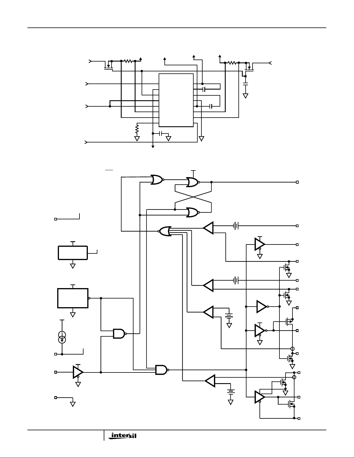
The HIP1011B creates a small and simple yet complete
power control solution to control the four independent
supplies (+5V, +3.3V, +12V, and -12V) found in PCI and
CompactPCI systems. For the +12V and -12V supplies,
overcurrent protection is provided internally with integrated
current sensing FET switches. For the +5V and +3.3V
supplies, overcurrent protection is provided by sensing the
voltage across the external current-sense resistors. The
PWRON input controls the state of both internal and external
switches. During an overcurrent condition on any output, all
MOSFETs are latched-off and a LOW (0V) is asserted on
the FLTN output. The FLTN latch is cleared when the
PWRONinput is toggled low again. During initial power-up of
the main V
from turning on the switches, and the latch is held in the
Reset state until the V
User programmability of the overcurrent threshold, response
time and turn-on slew rate is provided. A resistor connected
to the OCSET pin programs the overcurrent thresholds. A
capacitor may be added to the FLTN pin to adjust the fault
reporting and power-supply latch-off response times after an
over-current event. Capacitors connected to the gate pins
determine the turn-on rate.
supply (+12V), the PWRON input is inhibited
CC
input is greater than 10V.
CC
File Number 4640.3
Features
• Allows for System Centralized Voltage Monitoring
• Adjustable Delay to Fault Notification and Latch-Off
• Controls Four Supplies: +5V, +3.3V, +12V, and -12V
• Internal MOSFET Switches for +12V and -12V Outputs
• µP Interface for On/Off Control and Fault Reporting
• Adjustable Overcurrent Protection for All Supplies
• Provides Overcurrent Fault Isolation
• Adjustable Turn-On Slew Rate
• Minimum Parts Count Solution
• No Charge Pump
Applications
• PCI Hot Plug
CompactPCI
•
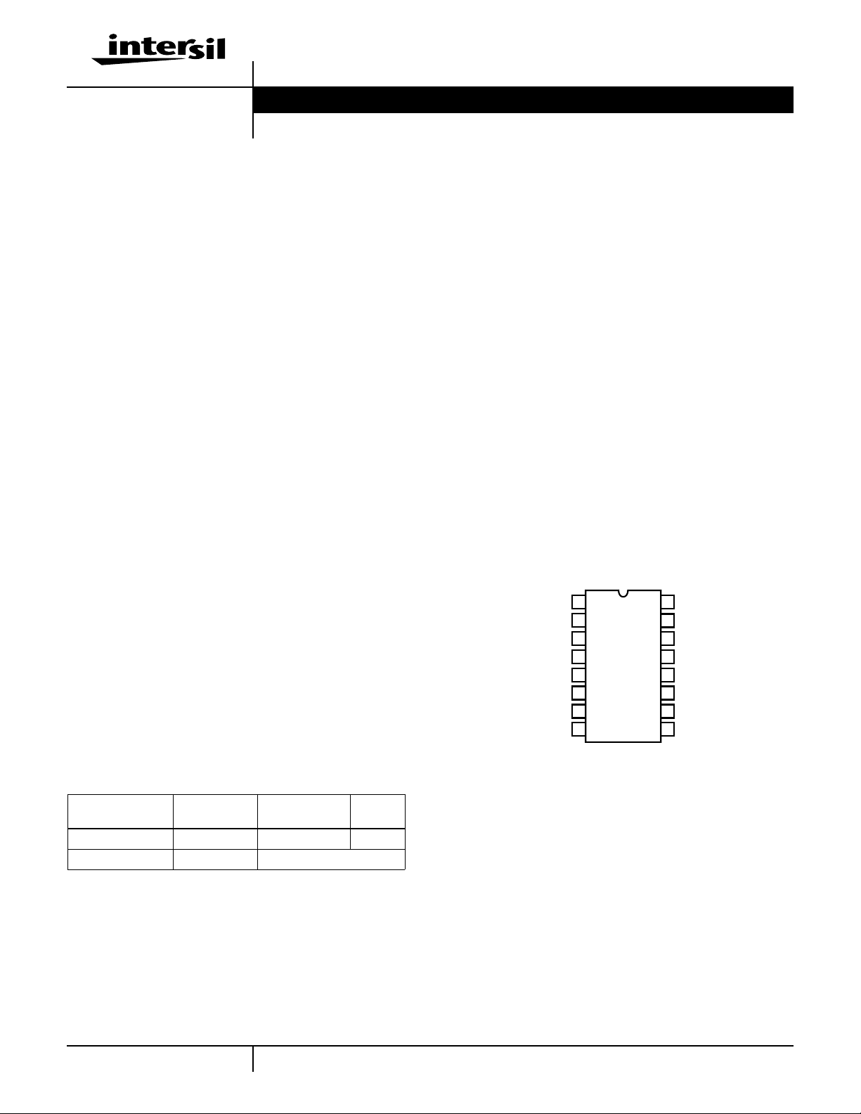
Pinout
HIP1011B
(SOIC)
TOP VIEW
M12VIN
FLTN
3V5VG
V
CC
12VIN
3VISEN
3VS
OCSET
1
2
3
4
5
6
7
8
16
15
14
13
12
11
10
9
M12VO
M12VG
12VG
GND
12VO
5VISEN
5VS
PWRON
Ordering Information
TEMP.RANGE
PART NUMBER
HIP1011BCB 0 to 70 16 Ld SOIC M16.15
HIP1011BCB-T 0 to 70 Tape and Reel
(oC) PACKAGE
1
PKG.
NO.
CAUTION: These devices are sensitive to electrostatic discharge; follow proper IC Handling Procedures.
1-888-INTERSIL or 321-724-7143
| Copyright © Intersil Corporation 2000

Typical Application
3.3V INPUT
-12V INPUT
12V INPUT
POWER CONTROL INPUT
FAULT OUTPUT (ACTIVE LOW)
Simplified Schematic
3.3V,
7.6A OUT
5mΩ, 1%
6.04kΩ
1%
SET (LOW = FAULT)
HIP1011B
12V,
0.5A OUT 0.1A OUT 5A OUT
HIP1011B
M12VIN
FLTN
3V5VG
V
12V
3VISEN
3VS
OCSET
M12VO
M12VG
CC
IN
5VISEN
PWRON
(OPTIONAL)
12VG
GND
12VO
5VS
V
CC
FAULT LATCH
5V,-12V,
0.033µF
0.033µF
NOTE:
ALL CAPACITORS ARE ±10%.
5mΩ, 1%
5V INPUT
HUF761315K8
0.033µF
LOW = FAULT
FLTN
V
CC
100µA
OCSET
PWRON
GND
V
V
CC
5V ZENER
REFERENCE
V
CC
12VIN
POWER-ON
RESET
V
CC
V
V
CC
5V
REF
LOW WHEN VCC < 10V
OCSET
CC
HIGH =
FAULT
RESET
COMP
COMP
COMP
HIGH = SWITCHES ON
COMP
V
OCSET
V
+
-
V
OCSET
+
-
V
OCSET
-
+
+
-
/3.3
OCSET
-
-
+
-
+
-
/13.3
/0.8
/17
+
V
CC
+
V
CC
0.3Ω
5VS
3V5VG
5VISEN
3VS
3VISEN
12VIN
12VG
12VO
M12VO
M12VG
0.7Ω
M12VIN
2

HIP1011B
Pin Descriptions
PIN DESIGNATOR FUNCTION DESCRIPTION
1 M12VIN -12V Input -12V Supply Input. Also provides power to the -12V overcurrent circuitry.
2 FLTN Fault Output 5V CMOS Fault Output; LOW = FAULT. A capacitor may be placed from this pin to ground to
provide delay time to fault notification and power supply latch-off.
3 3V5VG 3.3V/5V Gate
Output
4VCC12V VCC Input Connect to unswitched 12V supply.
5 12V
6 3VISEN 3.3V Current Sense Connect to the load side of the current sense resistor in series with source of external 3.3V
7 3VS 3.3V Source Connect to Source of 3.3V MOSFET. This connection along with pin 6 (3VISEN) senses the
8 OCSET Overcurrent Set Connect a resistor from this pin to ground to set the overcurrent trip point of all four switches. All
9 PWRON Power On Control Controls all Four Switches. High to Turn Switches ON, Low to turn them OFF.
10 5VS 5V Source Connectto Source of 5V MOSFET Switch. This connection along with pin 11 (5VISEN) senses
11 5VISEN 5V Current Sense Connectto the load side ofthe current sense resistor in serieswith source of external 5V MOSFET.
12 12VO Switched 12V
13 GND Ground Connect to common of power supplies.
14 12VG Gate of Internal
15 M12VG Gate of Internal
16 M12VO Switched -12V
IN
12V Input Switched 12V supply input.
Output
PMOS
NMOS
Output
Drive the Gates of the 3.3V and 5V MOSFETs. Connect a capacitor to ground to set the startup ramp. During turn on, this capacitor is charged with a 25µA current source.
MOSFET. This pin tied to GND when FET switch outputs disabled.
voltage drop across the sense resistor.
four over current trips can be programmed by changing the value of this resistor. The default
(6.04kΩ, 1%) is compatible with the maximum allowable currents as outlined in the PCI
specification.
the voltage drop across the sense resistor.
This pin tied to GND when FET switch outputs disabled.
Switched 12V output. This pin tied to GND when FET switch outputs disabled.
Connect a capacitor between 12VG and 12VO to set the start up ramp for the +12V supply.
This capacitor is charged with a 25µA current source during start-up.
Connect a capacitor between M12VG and M12VO to set the start-up ramp for the M12V
supply. This capacitor is charged with 25µA during start-up.
Switched 12V Output. This pin tied to GND when FET switch outputs disabled.
3
 Loading...