

®
www.BDTIC.com/Intersil
HIP1011
Data Sheet March 2004 FN4311.9
PCI Hot Plug Controller
The HIP1011 is the PCI Hot Plug voltage bus control IC for
use in modern computer systems that facilitates hot plugging
of adapter cards into and out of an active or passive back
plane. Along with discrete power MOSFETs and a few passive
components, the HIP1011 creates a small and simple yet
complete power control solution. Four independent supplies
are controlled, +5V, +3.3V, +12V, and -12V. The +12V and 12V switches are integrated. For the +5V and +3.3V supplies,
overcurrent protection is provided by sensing the voltage
across external current-sense resistors. For the +12V and
-12V supplies, overcurrent protection is provided internally. In
addition, an on-chip reference is used to monitor the +5V,
+3.3V and +12V outputs for undervoltage conditions. The
PWRON input controls the state of the switches. During an
overcurrent condition on any output, or an undervoltage
condition on the +5V, +3.3V or +12V outputs, all MOSFETs
are immediately latched-off and a LOW (0V) is asserted on
the FLTN output. The FLTN latch is cleared when the PWRON
input is toggled low again. During initial power-up of the main
V
supply (+12V), the PWRON input is inhibited from
CC
turning on the switches, and the latch is held in the Reset
state until the V
input is greater than 10V.
CC
User programmability of the overcurrent threshold and turn-on
slew rate is provided. A resistor connected to the OCSET pin
programs the overcurrent threshold. Capacitors connected to
the gate pins set the turn-on rate. Also, a capacitor may be
added to the FLTN pin to provide noise immunity.
Ordering Information
TEMP. RANGE
PART NUMBER
HIP1011CB 0 to 70 16 Ld SOIC M16.15
HIP1011CB-T 0 to 70 Tape and Reel
HIP1011CBZA
(Note)
HIP1011CBZA-T
(Note)
HIP1011EVAL1 Evaluation Platform
NOTE: Intersil Pb-free products employ special Pb-free material
sets; molding compounds/die attach materials and 100% matte tin
plate termination finish, which is compatible with both SnPb and
Pb-free soldering operations. Intersil Pb-free products are MSL
classified at Pb-free peak reflow temperatures that meet or exceed
the Pb-free requirements of IPC/JEDEC J Std-020B.
(°C) PACKAGE
0 to 70 16 Ld SOIC
(Pb-free)
0 to 70 Tape and Reel
(Pb-free)
PKG.
DWG. #
M16.15
Features
• Controls Distribution of Four Supplies: +5V, +3.3V, +12V,
and -12V
• Internal MOSFET Switches for +12V and -12V Outputs
• Microprocessor Interface for On/Off Control and Fault
Reporting
• Adjustable Overcurrent Protection for All Supplies
• Provides Fault Isolation
• Adjustable Turn-On Slew Rate
• Minimum Parts Count Solution
• No Charge Pump
• Pb-Free Package Options
Applications
• PCI Hot Plug
• CompactPCI
Pinout
HIP1011
(SOIC)
TOP VIEW
M12VIN
FLTN
3V5VG
V
CC
12VIN
3VISEN
3VS
OCSET
1
2
3
4
5
6
7
8
16
15
14
13
12
11
10
9
M12VO
M12VG
12VG
GND
12VO
5VISEN
5VS
PWRON
1
CAUTION: These devices are sensitive to electrostatic discharge; follow proper IC Handling Procedures.
1-888-INTERSIL or 321-724-7143
| Intersil (and design) is a registered trademark of Intersil Americas Inc.
All other trademarks mentioned are the property of their respective owners.
Copyright © Intersil Americas Inc. 2004. All Rights Reserved
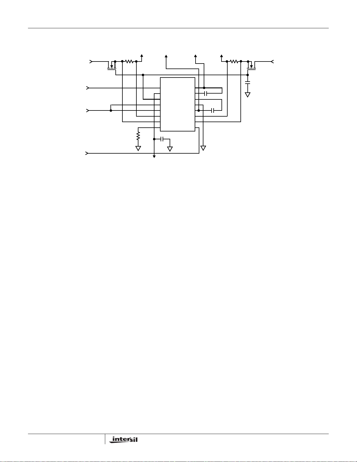
Typical Application
www.BDTIC.com/Intersil
3.3V INPUT
HIP1011
3.3V,
7.6A OUT 0.5A OUT 0.1A OUT 5A OUT
5mΩ, 1%
12V,
5V,-12V,
5mΩ, 1%
5V INPUT
HUF761315K8
-12V INPUT
12V INPUT
6.04kΩ
POWER CONTROL INPUT
HIP1011
M12VIN
FLTN
3V5VG
V
CC
12VIN
3VISEN
3VS
OCSET
1%
FAULT OUTPUT (ACTIVE LOW)
5VISEN
PWRON
(OPTIONAL)
M12VO
M12VG
12VG
GND
12VO
5VS
0.033µF
0.033µF
0.033µF
NOTE:
1. All capacitors are ±10%.
2
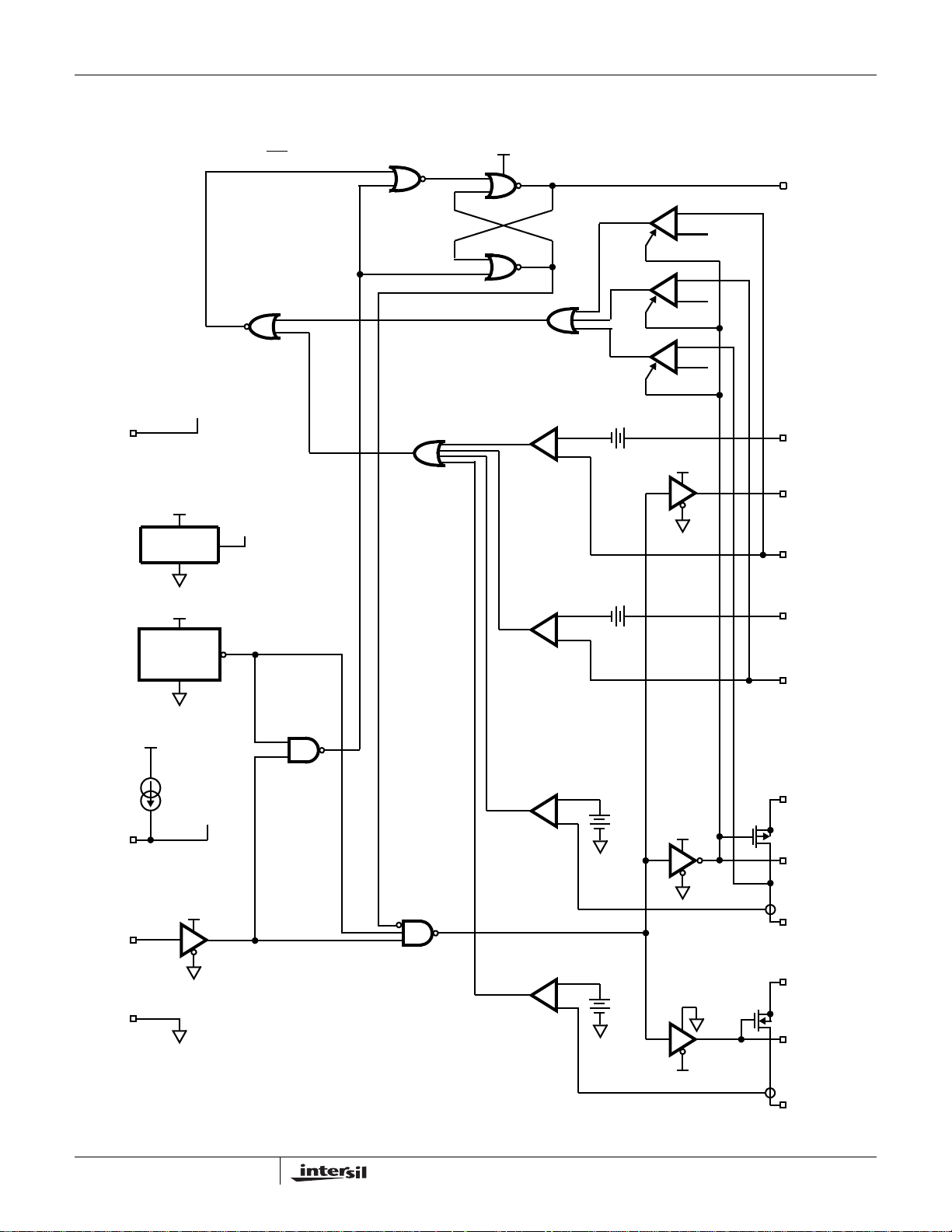
Simplified Schematic
www.BDTIC.com/Intersil
V
CC
V
CC
SET (LOW = FAULT)
HIP1011
RESET
5VREF
COMP
FAULT LATCH
+
-
V
OCSET
LOW = FAULT
COMP
COMP
COMP
/17
-
+
-
4.6V
+
INHIBIT
-
2.9V
+
INHIBIT
-
10.8V
+
INHIBIT
V
CC
FLTN
5VS
100µA
OCSET
PWRON
V
CC
5V ZENER
REFERENCE
V
CC
12VIN
POWER-ON
RESET
V
CC
V
V
OCSET
CC
5VREF
LOW WHEN V
CC
< 10V
HIGH =
FAU LT
V
OCSET
COMP
+
-
V
COMP
HIGH = SWITCHES ON
OCSET
+
-
3V5VG
5VISEN
/13.3
-
+
/0.8
+
V
CC
0.3Ω
3VS
3VISEN
12VIN
12VG
12VO
V
COMP
GND
OCSET
+
3
/3.3
+
-
M12VIN
0.7Ω
M12VIN
M12VG
M12VO

HIP1011
www.BDTIC.com/Intersil
Pin Descriptions
PIN DESIGNATOR FUNCTION DESCRIPTION
1 M12VIN -12V Input -12V Supply Input. Also provides power to the -12V overcurrent circuitry.
2 FLTN Fault Output 5V CMOS Fault Output; LOW = FAULT. An optional capacitor may be place from this pin to
ground to provide additional immunity from power supply glitches.
3 3V5VG 3.3V/5V Gate Output Drive the gates of the 3.3V and 5V MOSFETs. Connect a capacitor to ground to set the startup
4 VCC 12V V
5 12VIN 12V Input Switched 12V supply input.
6 3VISEN 3.3V Current Sense Connect to the load side of the current sense resistor in series with source of external 3.3V
7 3VS 3.3V Source Connect to source of 3.3V MOSFET. This connection along with pin 6 (3VISEN) senses the
8 OCSET Overcurrent Set Connect a resistor from this pin to ground to set the overcurrent trip point of all four switches. All
9 PWRON Power On Control Controls all four switches. High to Turn Switches ON, Low to turn them OFF.
10 5VS 5V Source Connect to source of 5V MOSFET switch. This connection along with pin 11(5VISEN) senses
11 5VISEN 5V Current Sense Connect to the load side of the current sense resistor in series with source of external 5V MOSFET.
12 12VO Switched 12V Output Switched 12V output.
13 GND Ground Connect to common of power supplies.
14 12VG Gate of Internal
15 M12VG Gate of Internal
16 M12VO Switched -12V
Input Connect to unswitched 12V supply.
CC
PMOS
NMOS
Output
ramp. During turn on, this capacitor is charged with a 25µA current source.
MOSFET.
voltage drop across the sense resistor.
four over current trips can be programmed by changing the value of this resistor. The default
(6.04kΩ, 1%) is compatible with the maximum allowable currents as outlined in the PCI
specification.
the voltage drop across the sense resistor.
Connect a capacitor between 12VG and 12VO to set the startup ramp for the +12V supply. This
capacitor is charged with a 25µA current source during startup. The 3.3V and 5V UV circuitry
is enabled after the voltage on 12VG is less than 400mV. Therefore, if the capacitor on the pin
3 (3V5VG) is more than 25% larger than the capacitor on pin 14 (12VG) a false UV may be
detected during startup.
Connect a capacitor between M12VG and M12VO to set the startup ramp for the M12V supply.
This capacitor is charged with 25µA during startup.
Switched 12V Output.
4

HIP1011
www.BDTIC.com/Intersil
Absolute Maximum Ratings Thermal Information
VCC, 12VIN . . . . . . . . . . . . . . . . . . . . . . . . . . . . . . . -0.5V to +14.0V
12VO . . . . . . . . . . . . . . . . . . . . . . . . . . . . . . . -0.5V to V
12VO, 12VG, 3V5VG . . . . . . . . . . . . . . . . . . . . . -0.5V to V
M12VIN . . . . . . . . . . . . . . . . . . . . . . . . . . . . . . . . . . -15.0V to +0.5V
M12VO, M12VG. . . . . . . . . . . . . . . . . . . . . V
3VISEN, 5VISEN . . . . . . . . . . . -0.5V to the lesser of V
Voltage, Any Other Pin. . . . . . . . . . . . . . . . . . . . . . . . -0.5V to +7.0V
12VO Output Current . . . . . . . . . . . . . . . . . . . . . . . . . . . . . . . . . . 3A
M12VO Output Current . . . . . . . . . . . . . . . . . . . . . . . . . . . . . . . 0.8A
ESD Classification . . . . . . . . . . . . . . . . . . . . . . . . . . . . 4KeV (HBM)
M12VIN
-0.5V to +0.5V
12VIN
CC
or +7.0V
CC
+0.5V
+0.5V
Operating Conditions
VCC Supply Voltage Range. . . . . . . . . . . . . . . . . +10.8V to +13.2V
±12V, 5V and 3.3V Input Supply Tolerances . . . . . . . . . . . . . . ±10%
12VO Output Current . . . . . . . . . . . . . . . . . . . . . . . . . . . . 0 to +0.5A
M12VO Output Current . . . . . . . . . . . . . . . . . . . . . . . . . . 0 to +0.1A
Temperature Range (T
CAUTION: Stresses above those listed in “Absolute Maximum Ratings” may cause permanent damage to the device. This is a stress only rating and operation of the
device at these or any other conditions above those indicated in the operational sections of this specification is not implied.
NOTES:
1. θ
is measured in free air with the component mounted on a high effective thermal conductivity test board in free air. See Technical Brief 379
JA
for details.
2. All voltages are relative to GND, unless otherwise specified.
) . . . . . . . . . . . . . . . . . . . . . . . . 0°C to 70°C
A
Thermal Resistance (Typical, Note 1)
SOIC Package . . . . . . . . . . . . . . . . . . . . . . . . . . . . . 68
Maximum Junction Temperature . . . . . . . . . . . . . . . . . . . . . . 125°C
Maximum Storage Temperature Range . . . . . . . . . . -65°C to 150°C
Maximum Lead Temperature (Soldering 10s) . . . . . . . . . . . . 300°C
(SOIC - Lead Tips Only)
θ
JA
(°C/W)
Die Characteristics
Number of Transistors . . . . . . . . . . . . . . . . . . . . . . . . . . . . . . . . 290
Electrical Specifications Nominal 5V and 3.3V Input Supply Voltages,
= 12VIN = 12V, M12VIN = -12V, TA = T
V
CC
PARAMETER SYMBOL TEST CONDITIONS MIN TYP MAX UNITS
5V/3.3V SUPPLY CONTROL
5V Overcurrent Threshold I
5V Overcurrent Threshold Voltage V
5V Undervoltage Trip Threshold V
5V Undervoltage Fault Response Time t
5V Turn-On Time (PWRON High to
5VOUT = 4.75V)
5VS Input Bias Current IB
5VISEN Input Bias Current IB
3V Overcurrent Threshold I
3V Overcurrent Threshold Voltage V
3V Undervoltage Trip Threshold V
3V Undervoltage Fault Response Time t
3V Turn-On Time (PWRON High to
3VOUT = 3.00V)
3VS Input Bias Current IB
3VISEN Input Bias Current IB
Gate Output Charge Current IC
Gate Turn-On Time (PWRON High to
3V5VG = 11V)
Gate Turn-Off Time t
Gate Turn-Off Time C
OC5V
OC5V
5VUV
5VUV
5VS
5VISEN
OC3V
OC3V
3VUV
3VUV
3VS
3VISEN
3V5VG
t
ON3V5V
OFF3V5V
See Figure 1, Typical Application - 7.1 - A
V
C
R
PWRON = High -40 -26 -20 µA
PWRON = High -160 -140 -110 µA
See Figure 1, Typical Application - 9.0 - A
V
C
R
PWRON = High -40 -26 -20 µA
PWRON = High -160 -140 -110 µA
PWRON = High, V
C
C
10%
= 1.2V 66 72 79 mV
OCSET
= 0.022µF, C
3V5VG
= 1Ω
L
= 1.2V 88 95 102 mV
OCSET
= 0.022µF, C
3V5VG
= 0.43Ω
L
= 0.1µF - 280 500 µs
3V5VG
= 0.1µF, 3V5VG from 9.5 V to 1V - 13 17 µs
3V5VG
= 0.022µF, 3V5VG Falling 90% to
3V5VG
= 0 to 70°C, Unless Otherwise Specified
J
4.42 4.6 4.75 V
- 150 350 ns
= 2000µF,
5VOUT
= 2000µF,
3VOUT
= 2V 22.5 25.0 27.5 µA
3V5VG
-6.5- ms
2.74 2.86 2.97 V
- 150 350 ns
-6.5- ms
-2-µs
5

HIP1011
www.BDTIC.com/Intersil
Electrical Specifications Nominal 5V and 3.3V Input Supply Voltages,
= 12VIN = 12V, M12VIN = -12V, TA = T
V
CC
PARAMETER SYMBOL TEST CONDITIONS MIN TYP MAX UNITS
+12V SUPPLY CONTROL
On Resistance of Internal PMOS r
Overcurrent Threshold I
12V Undervoltage Trip Threshold V
Undervoltage Fault Response Time t
Gate Charge Current IC
Turn-On Time (PWRON High to
12VG = 1V)
Turn-O ff Time t
Turn-O ff Time C
-12V SUPPLY CONTROL
On Resistance of Internal NMOS r
Overcurrent Threshold I
Gate Output Charge Current IC
Turn-On Time (PWRON High to
M12VG = -1V)
Turn-On Time (PWRON High to
M12VO = -10.8V)
Turn-O ff Time t
Turn-O ff Time C
M12VIN Input Bias Current IB
CONTROL I/O PINS
Supply Current I
OCSET Current I
Overcurrent Fault Response Time t
PWRON Threshold Voltage V
FLTN Output Low Voltage V
FLTN Output High Voltage V
FLTN Output Latch Threshold V
12V Power On Reset Threshold V
DS(ON)12
OC12V
12VUV
12VUV
12VG
t
ON12V
OFF12V
DS(ON)M12
OCM12V
M12VG
t
ONM12V
OFFM12V
M12VIN
VCC
OCSET
OC
THPWRON
FLTN,OLIFLTN
FLTN,OHIFLTN
FLTN,TH
POR,TH
PWRON = High, ID = 0.5A, TA = TJ = 25°C 0.18 .300 0.350 Ω
V
PWRON = High, V
C
C
10% - 90%
PWRON = High, ID = 0.1A,
T
V
PWRON = High, V
C
C
R
C
to 10%
PWRON = High - 2 2.6 mA
VCC Voltage Falling 9.4 10 10.6 V
= 1.2V 1.25 1.50 1.8 A
OCSET
= 0.022µF - 16 20 ms
12VG
= 0.1µF, 12VG - 9 12 µs
12VG
= 0.022µF, 12VG Rising
12VG
= TJ = 25°C
A
= 1.2V 0.30 0.37 0.50 A
OCSET
= 0.022µF - 160 300 µs
M12VG
= 0.022µF, C
M12VG
= 120Ω
L
= 0.1µF, M12VG - 18 23 µs
M12VG
= 0.022µF, M12VG Falling 90%
M12VG
= 2mA - 0.6 0.9 V
= 0 to -4mA 3.9 4.3 4.9 V
= 0 to 70°C, Unless Otherwise Specified (Continued)
J
10.5 10.8 11.15 V
- 150 - ns
= 3V 23.5 25.0 28.5 µA
12VG
-3-µs
0.5 0.7 0.9 Ω
= -4V 22.5 25 27.5 µA
M12VG
M12VO
= 50µF,
-16-ms
-3-µs
455.8mA
95 100 105 µA
- 500 960 ns
0.8 1.6 2.1 V
1.8 2.3 3 V
6

Typical Performance Curves
www.BDTIC.com/Intersil
HIP1011
340
320
+12 (mΩ)
ON
300
PMOS r
280
260
0 5 10 15 20 25 30 35 40 45 50 55 60 65 70
NMOS -12 r
ON
PMOS +12 r
TEMPERATURE (°C)
ON
FIGURE 1. rON vs TEMPERATURE FIGURE 2. UV TRIP vs TEMPERATURE
10.84
10.83
1000
900
800
700
600
-12 (mΩ)
ON
NMOS r
4.632
4.631
4.630
4.629
5V UVTRIP (V)
4.628
4.627
4.626
0 5 10 15 20 25 30 35 40 45 50 55 60 65 70
TEMPERATURE (°C)
100
90
3V OCVth
5 UV
3.3 UV
2.862
2.861
2.860
3.3V UVTRIP (V)
2.859
2.858
12 UV TRIP (V)
10.82
10.81
0 5 10 15 20 25 30 35 40 45 50 55 60 65 70
TEMPERATURE (°C)
FIGURE 3. 12 UV TRIP vs TEMPERATURE FIGURE 4. OCVth vs TEMPERATURE (VR
102
101
100
IOC SET (µA)
99
98
0 5 10 15 20 25 30 35 40 45 50 55 60 65 70
80
OC Vth (mV)
70
60
0 5 10 15 20 25 30 35 40 45 50 55 60 65 70
TEMPERATURE (°C)
FIGURE 5. OCSET I vs TEMPERATURE
TEMPERATURE (°C)
5V OCVth
OCSET
= 1.21V)
7

HIP1011
www.BDTIC.com/Intersil
Small Outline Plastic Packages (SOIC)
N
INDEX
AREA
123
-A-
D
e
B
0.25(0.010) C AMB
NOTES:
1. Symbols are defined in the “MO Series Symbol List” in Section
2.2 of Publication Number 95.
2. Dimensioning and tolerancing per ANSI Y14.5M-1982.
3. Dimension “D” does not include mold flash, protrusions or gate
burrs. Mold flash, protrusion and gate burrs shall not exceed
0.15mm (0.006 inch) per side.
4. Dimension “E” does not include interlead flash or protrusions. Interlead flash and protrusions shall not exceed 0.25mm (0.010
inch) per side.
5. The chamfer on the body is optional. If it is not present, a visual
index feature must be located within the crosshatched area.
6. “L” is the length of terminal for soldering to a substrate.
7. “N” is the number of terminal positions.
8. Terminal numbers are shown for reference only.
9. The lead width “B”, as measured 0.36mm (0.014 inch) or greater
above the seating plane, shall not exceed a maximum value of
0.61mm (0.024 inch)
10. Controlling dimension: MILLIMETER. Converted inch dimensions are not necessarily exact.
E
-B-
SEATING PLANE
A
-C-
S
M
0.25(0.010) B
H
α
µ
A1
0.10(0.004)
M
L
h x 45
M
o
M16.15 (JEDEC MS-012-AC ISSUE C)
16 LEAD NARROW BODY SMALL OUTLINE PLASTIC PACKAGE
INCHES MILLIMETERS
SYMBOL
A 0.053 0.069 1.35 1.75 -
A1 0.004 0.010 0.10 0.25 -
B 0.014 0.019 0.35 0.49 9
C 0.007 0.010 0.19 0.25 -
D 0.386 0.394 9.80 10.00 3
E 0.150 0.157 3.80 4.00 4
e 0.050 BSC 1.27 BSC -
H 0.228 0.244 5.80 6.20 -
h 0.010 0.020 0.25 0.50 5
C
L 0.016 0.050 0.40 1.27 6
N16 167
α
0° 8° 0° 8° -
NOTESMIN MAX MIN MAX
Rev. 1 02/02
All Intersil U.S. products are manufactured, assembled and tested utilizing ISO9000 quality systems.
Intersil Corporation’s quality certifications can be viewed at www.intersil.com/design/quality
Intersil products are sold by description only. Intersil Corporation reserves the right to make changes in circuit design, software and/or specifications at any time without
notice. Accordingly, the reader is cautioned to verify that data sheets are current before placing orders. Information furnished by Intersil is believed to be accurate and
reliable. However, no responsibility is assumed by Intersil or its subsidiaries for its use; nor for any infringements of patents or other rights of third parties which may result
from its use. No license is granted by implication or otherwise under any patent or patent rights of Intersil or its subsidiaries.
For information regarding Intersil Corporation and its products, see www.intersil.com
8
 Loading...