

HIP1011
Data Sheet August 1999 File Number 4311.7
PCI Hot Plug Controller
The HIP1011 is the PCI Hot Plug voltage bus control IC f or
use in modern computer systems that facilitates hot plugging
of adapter cards into and out of an active or passive back
plane. Along with discrete power MOSFETs and a few
passivecomponents, the HIP1011 creates a small and simple
yet complete power control solution. F our independent
supplies are controlled, +5V, +3.3, +12V, and -12V. The +12V
and -12V switches are integrated. F or the +5V and +3.3V
supplies, overcurrent protection is provided by sensing the
voltage across external current-sense resistors. For the +12V
and -12V supplies, overcurrent protection is provided
internally . In addition, an on-chip reference is used to monitor
the +5V, +3.3V and +12V outputs for undervoltage conditions.
The PWRON input controls the state of the switches. During
an overcurrent condition on any output, or an undervoltage
condition on the +5V, +3.3V or +12V outputs, all MOSFETs
are immediately latched-off and a LOW (0V) is asserted on
the FLTN output. The FLTNlatchiscleared when the PWRON
input is toggled low again. During initial power-up of the main
supply (+12V), the PWRON input is inhibited from
V
CC
turning on the switches, and the latch is held in the Reset
state until the V
input is greater than 10V.
CC
User programmability of the overcurrent threshold and turn-on
slew rate is provided. A resistor connected to the OCSET pin
programs the overcurrent threshold. Capacitors connected to
the gate pins set the turn-on rate. Also, a capacitor may be
added to the FLTN pin to provide noise immunity.
Ordering Information
TEMP.
PART NUMBER
HIP1011CB 0 to 70 16 Ld SOIC M16.15
HIP1011CB-T 0 to 70 Tape and Reel
RANGE (oC) PACKAGE
PKG.
NO.
Features
• Controls Distribution of Four Supplies: +5V, +3.3V, +12V,
and -12V
• Internal MOSFET Switches for +12V and -12V Outputs
• Microprocessor Interface for On/Off Control and Fault
Reporting
• Adjustable Overcurrent Protection for All Supplies
• Provides Fault Isolation
• Adjustable Turn-On Slew Rate
• Minimum Parts Count Solution
• No Charge Pump
Applications
• PCI Hot Plug
• CompactPCI
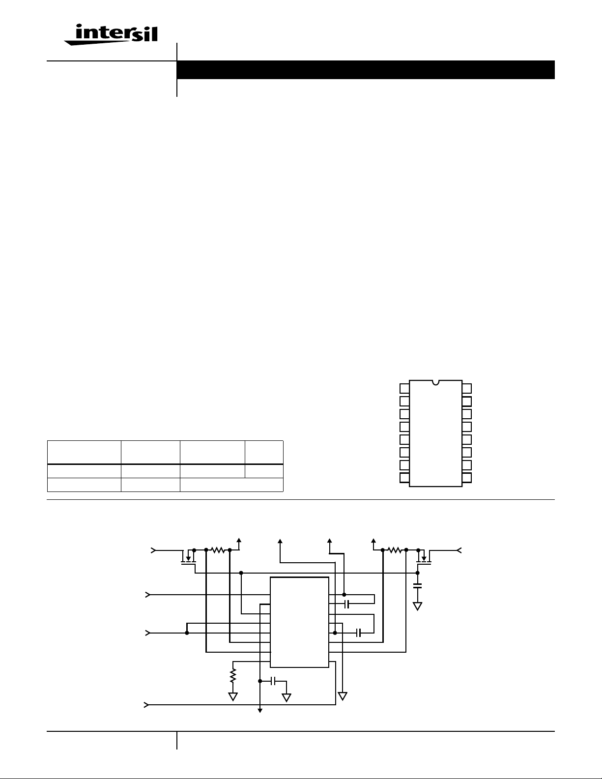
Pinout
HIP1011
(SOIC)
TOP VIEW
M12VIN
FLTN
3V5VG
V
CC
12VIN
3VISEN
3VS
OCSET
1
2
3
4
5
6
7
8
16
15
14
13
12
11
10
9
M12VO
M12VG
12VG
GND
12VO
5VISEN
5VS
PWRON
Typical Application
3.3V INPUT
-12V INPUT
12V INPUT
POWER CONTROL INPUT
2-1
3.3V,
7.6A OUT 0.5A OUT 0.1A OUT 5A OUT
5mΩ, 1%
6.04kΩ
1%
FAULT OUTPUT (ACTIVE LOW)
CAUTION: These devices are sensitive to electrostatic discharge; follow proper IC Handling Procedures.
12V,
HIP1011
M12VIN
FLTN
3V5VG
V
CC
12VIN
3VISEN
3VS
OCSET
(OPTIONAL)
M12VO
M12VG
12VG
GND
12VO
5VISEN
5VS
PWRON
1-888-INTERSIL or 321-724-7143
5V,-12V,
5mΩ, 1%
0.033µF
0.033µF
NOTE:
1. All capacitors are ±10%.
5V INPUT
HUF761315K8
0.033µF
| Copyright © Intersil Corporation 1999
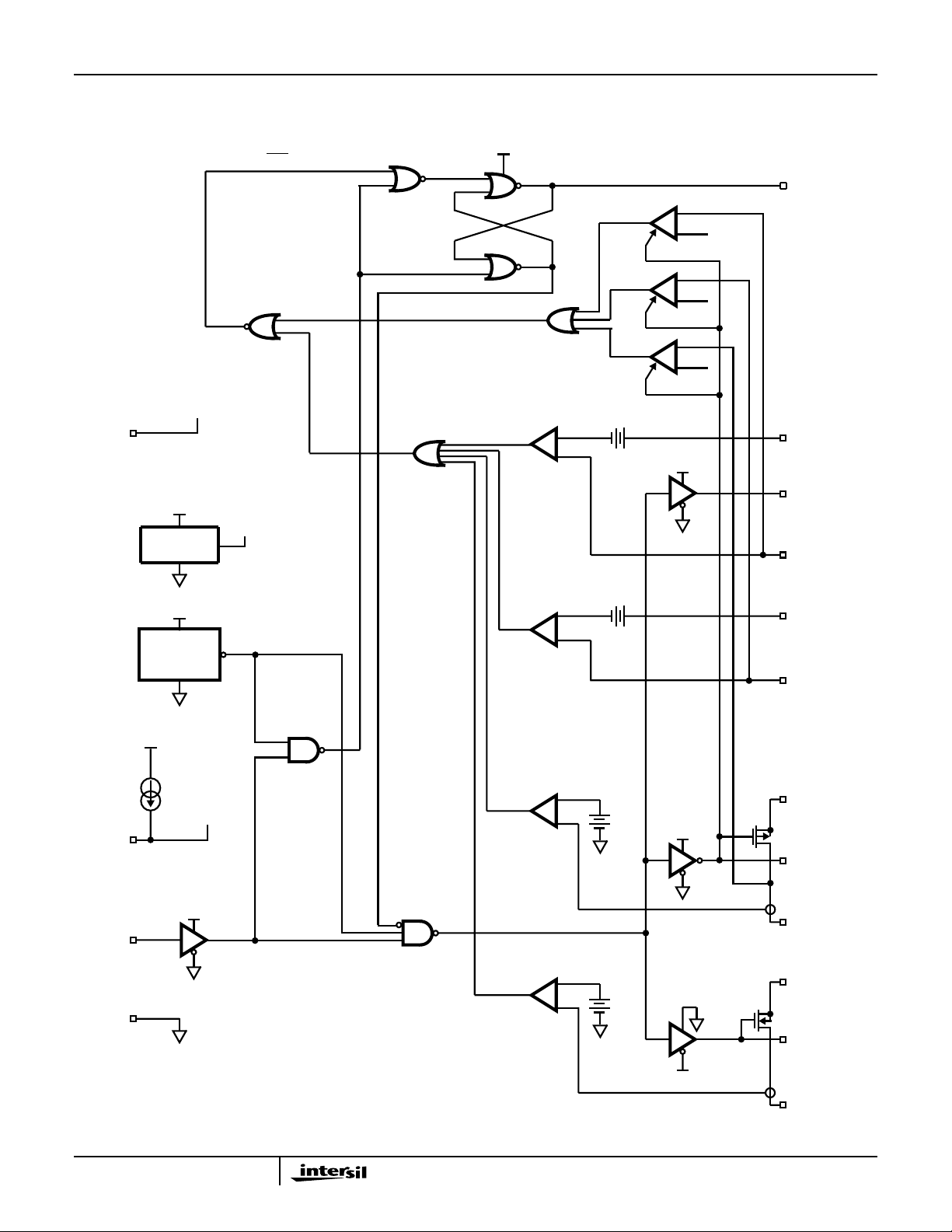
Simplified Schematic
V
CC
V
CC
SET (LOW = FAULT)
HIP1011
RESET
5VREF
COMP
FAULT LATCH
+
-
V
OCSET
LOW = FAULT
COMP
COMP
COMP
/17
-
+
-
+
INHIBIT
-
+
INHIBIT
-
+
INHIBIT
V
CC
FLTN
4.6V
2.9V
10.8V
5VS
100µA
OCSET
PWRON
V
CC
5V ZENER
REFERENCE
V
CC
12VIN
POWER-ON
RESET
V
CC
V
V
OCSET
CC
5VREF
LOW WHEN V
CC
< 10V
HIGH =
FAULT
V
OCSET
COMP
+
-
V
COMP
OCSET
-
+
-
HIGH = SWITCHES ON
3V5VG
5VISEN
/13.3
-
+
/0.8
+
V
CC
0.3Ω
3VS
3VISEN
12VIN
12VG
12VO
GND
2-2
COMP
V
/3.3
OCSET
+
-
+
-
M12VIN
0.7Ω
M12VIN
M12VG
M12VO

HIP1011
Pin Descriptions
PIN DESIGNATOR FUNCTION DESCRIPTION
1 M12VIN -12V Input -12V Supply Input. Also provides power to the -12V overcurrent circuitry.
2 FLTN Fault Output 5V CMOS Fault Output; LOW = FAULT. An optional capacitor may be place from this pin to
ground to provide additional immunity from power supply glitches.
3 3V5VG 3.3V/5V Gate Output Drive the gates of the 3.3V and 5V MOSFETs. Connect a capacitor to ground to set the start-
up ramp. During turn on, this capacitor is charged with a 25µA current source.
4 VCC 12V VCC Input Connect to unswitched 12V supply.
5 12VIN 12V Input Switched 12V supply input.
6 3VISEN 3.3V Current Sense Connect to the load side of the current sense resistor in series with source of external 3.3V
MOSFET.
7 3VS 3.3V Source Connect to source of 3.3V MOSFET. This connection along with pin 6 (3VISEN) senses the
voltage drop across the sense resistor.
8 OCSET Overcurrent Set Connect a resistor from this pin to ground to set the overcurrent trip point of all four switches. All
four over current trips can be programmed by changing the value of this resistor. The default
(6.04kΩ, 1%) is compatible with the maximum allowable currents as outlined in the PCI specifi-
cation.
9 PWRON Power On Control Controls all four switches. High to Turn Switches ON, Low to turn them OFF.
10 5VS 5V Source Connect to source of 5V MOSFET switch. This connection along with pin 11(5VISEN) senses
the voltage drop across the sense resistor.
11 5VISEN 5V Current Sense Connectto the load side of the current senseresistorinserieswithsourceof external 5V MOSFET .
12 12VO Switched 12V Output Switched 12V output.
13 GND Ground Connect to common of power supplies.
14 12VG Gate of Internal
PMOS
15 M12VG Gate of Internal
NMOS
16 M12VO Switched -12V
Output
Connect a capacitor between 12VG and 12VO to set the start up ramp for the +12V supply.
This capacitor is charged with a 25µA current source during start -up. The 3.3V and 5V UV
circuitry is enabled after the voltage on 12VG is less than 400mV. Therefore, if the capacitor
on the pin 3 (3V5VG) is more than 25% larger than the capacitor on pin 14 (12VG) a false UV
may be detected during start up.
Connectacapacitorbetween M12VG andM12VOto set the startupramp for the M12Vsupply.
This capacitor is charged with 25µA during start up.
Switched 12V Output.
2-3

HIP1011
Absolute Maximum Ratings Thermal Information
VCC, 12VIN . . . . . . . . . . . . . . . . . . . . . . . . . . . . . . . -0.5V to +14.0V
12VO . . . . . . . . . . . . . . . . . . . . . . . . . . . . . . . -0.5V to V
12VIN
+0.5V
12VO, 12VG, 3V5VG . . . . . . . . . . . . . . . . . . . . . -0.5V to VCC+0.5V
M12VIN . . . . . . . . . . . . . . . . . . . . . . . . . . . . . . . . . . -15.0V to +0.5V
M12VO, M12VG. . . . . . . . . . . . . . . . . . . . . V
M12VIN
-0.5V to +0.5V
3VISEN, 5VISEN . . . . . . . . . . . -0.5V to the lesser of VCC or +7.0V
Voltage, Any Other Pin. . . . . . . . . . . . . . . . . . . . . . . . -0.5V to +7.0V
12VO Output Current. . . . . . . . . . . . . . . . . . . . . . . . . . . . . . . . . . 3A
M12VO Output Current . . . . . . . . . . . . . . . . . . . . . . . . . . . . . . . 0.8A
ESD Classification . . . . . . . . . . . . . . . . . . . . . . . . . . . . 4KeV (HBM)
Operating Conditions
VCC Supply Voltage Range. . . . . . . . . . . . . . . . . +10.8V to +13.2V
±12V, 5V and 3.3V Input Supply Tolerances . . . . . . . . . . . . . . ±10%
12VO Output Current. . . . . . . . . . . . . . . . . . . . . . . . . . . . 0 to +0.5A
M12VO Output Current . . . . . . . . . . . . . . . . . . . . . . . . . . 0 to +0.1A
Temperature Range (TA) . . . . . . . . . . . . . . . . . . . . . . . 0oC to 70oC
CAUTION: Stresses above those listed in “Absolute Maximum Ratings” may cause permanent damage to the device. This is a stress only rating and operation of the
device at these or any other conditions above those indicated in the operational sections of this specification is not implied.
NOTES:
1. θJA is measured with the component mounted on an evaluation PC board in free air.
2. All voltages are relative to GND, unless otherwise specified.
Thermal Resistance (Typical, Note 1) θJA (oC/W)
SOIC Package . . . . . . . . . . . . . . . . . . . . . . . . . . . . . 100
Maximum Junction Temperature . . . . . . . . . . . . . . . . . . . . . . 125oC
Maximum Storage Temperature Range. . . . . . . . . . -65oC to 150oC
Maximum Lead Temperature (Soldering 10s) . . . . . . . . . . . . 300oC
(SOIC - Lead Tips Only)
Die Characteristics
Number of Transistors . . . . . . . . . . . . . . . . . . . . . . . . . . . . . . . . 290
Electrical Specifications Nominal 5V and 3.3V Input Supply Voltages,
VCC = 12VIN = 12V, M12VIN = -12V, TA = TJ= 0 to 70oC, Unless Otherwise Specified
PARAMETER SYMBOL TEST CONDITIONS MIN TYP MAX UNITS
5V/3.3V SUPPLY CONTROL
5V Overcurrent Threshold I
5V Overcurrent Threshold Voltage V
5V Undervoltage Trip Threshold V
5V Undervoltage Fault Response Time t
OC5V
OC5V
5VUV
5VUV
5V Turn-On Time (PWRON High to
5VOUT = 4.75V)
5VS Input Bias Current IB
5VISEN Input Bias Current IB
3V Overcurrent Threshold I
3V Overcurrent Threshold Voltage V
3V Undervoltage Trip Threshold V
3V Undervoltage Fault Response Time t
5VS
5VISEN
OC3V
OC3V
3VUV
3VUV
3V Turn-On Time (PWRON High to
3VOUT = 3.00V)
3VS Input Bias Current IB
3VISEN Input Bias Current IB
Gate Output Charge Current IC
Gate Turn-On Time (PWRON High to
3VS
3VISEN
3V5VG
t
ON3V5V
3V5VG = 11V)
Gate Turn-Off Time t
OFF3V5V
Gate Turn-Off Time C
See Figure 1, Typical Application - 7.1 - A
V
= 1.2V 66 72 79 mV
OCSET
C
= 0.022µF, C
3V5VG
RL = 1Ω
PWRON = High -40 -26 -20 µA
PWRON = High -160 -140 -110 µA
See Figure 1, Typical Application - 9.0 - A
V
= 1.2V 88 95 102 mV
OCSET
C
= 0.022µF, C
3V5VG
RL = 0.43Ω
PWRON = High -40 -26 -20 µA
PWRON = High -160 -140 -110 µA
PWRON = High, V
C
= 0.1µF - 280 500 µs
3V5VG
C
= 0.1µF, 3V5VG from 9.5 V to 1V - 13 17 µs
3V5VG
=0.022µF,3V5VGFalling 90% to
3V5VG
10%
4.42 4.6 4.75 V
- 150 350 ns
5VOUT
= 2000µF,
- 6.5 - ms
2.74 2.86 2.97 V
- 150 350 ns
= 2000µF,
3VOUT
= 2V 22.5 25.0 27.5 µA
3V5VG
- 6.5 - ms
-2-µs
2-4

HIP1011
Electrical Specifications Nominal 5V and 3.3V Input Supply Voltages,
VCC = 12VIN = 12V, M12VIN = -12V, TA = TJ= 0 to 70oC, Unless Otherwise Specified (Continued)
PARAMETER SYMBOL TEST CONDITIONS MIN TYP MAX UNITS
+12V SUPPLY CONTROL
On Resistance of Internal PMOS r
Overcurrent Threshold I
12V Undervoltage Trip Threshold V
Undervoltage Fault Response Time t
Gate Charge Current IC
Turn-On Time (PWRON High to
DS(ON)12
OC12V
12VUV
12VUV
12VG
t
ON12V
12VG = 1V)
Turn-Off Time t
OFF12V
Turn-Off Time C
-12V SUPPLY CONTROL
On Resistance of Internal NMOS r
Overcurrent Threshold I
Gate Output Charge Current IC
Turn-On Time (PWRON High to
DS(ON)M12
OCM12V
M12VG
t
ONM12V
M12VG = -1V)
Turn-On Time (PWRON High to
M12VO = -10.8V)
Turn-Off Time t
OFFM12V
Turn-Off Time C
M12VIN Input Bias Current IB
M12VIN
CONTROL I/O PINS
Supply Current I
OCSET Current I
Overcurrent Fault Response Time t
PWRON Threshold Voltage V
FLTN Output Low Voltage V
FLTN Output High Voltage V
FLTN Output Latch Threshold V
12V Power On Reset Threshold V
VCC
OCSET
OC
THPWRON
FLTN,OLIFLTN
FLTN,OHIFLTN
FLTN,TH
POR,TH
PWRON = High, ID= 0.5A, TA=TJ=25oC 0.18 .300 0.350 Ω
V
= 1.2V 1.25 1.50 1.8 A
OCSET
PWRON = High, V
C
= 0.022µF - 16 20 ms
12VG
C
= 0.1µF, 12VG - 9 12 µs
12VG
= 0.022µF, 12VG Rising
12VG
10% - 90%
PWRON = High, ID = 0.1A,
TA = TJ = 25oC
V
= 1.2V 0.30 0.37 0.50 A
OCSET
PWRON = High, V
C
= 0.022µF - 160 300 µs
M12VG
C
= 0.022µF, C
M12VG
RL = 120Ω
C
= 0.1µF, M12VG - 18 23 µs
M12VG
= 0.022µF, M12VG Falling 90%
M12VG
to 10%
PWRON = High - 2 2.6 mA
= 2mA - 0.6 0.9 V
= 0 to -4mA 3.9 4.3 4.9 V
VCC Voltage Falling 9.4 10 10.6 V
10.5 10.8 11.15 V
- 150 - ns
= 3V 23.5 25.0 28.5 µA
12VG
-3-µs
0.5 0.7 0.9 Ω
= -4V 22.5 25 27.5 µA
M12VG
M12VO
= 50µF,
-16-ms
-3-µs
4 5 5.8 mA
95 100 105 µA
- 500 960 ns
0.8 1.6 2.1 V
1.8 2.3 3 V
2-5

Typical Performance Curves
HIP1011
340
320
+12 (mΩ)
ON
300
PMOS r
280
260
0 5 10 15 20 25 30 35 40 45 50 55 60 65 70
NMOS -12 r
ON
PMOS +12 r
TEMPERATURE (oC)
ON
FIGURE 1. rON vs TEMPERATURE FIGURE 2. UV TRIP vs TEMPERATURE
10.84
10.83
1000
900
800
700
600
-12 (mΩ)
ON
NMOS r
4.632
4.631
4.630
4.629
5V UVTRIP (V)
4.628
4.627
4.626
0 5 10 15 20 25 30 35 40 45 50 55 60 65 70
TEMPERATURE (oC)
100
90
3V OCVth
5 UV
3.3 UV
2.862
2.861
2.860
3.3V UVTRIP (V)
2.859
2.858
12 UV TRIP (V)
10.82
10.81
0 5 10 15 20 25 30 35 40 45 50 55 60 65 70
TEMPERATURE (oC)
FIGURE 3. 12 UV TRIP vs TEMPERATURE FIGURE 4. OCVth vs TEMPERATURE (VR
102
101
100
IOC SET (µA)
99
98
0 5 10 15 20 25 30 35 40 45 50 55 60 65 70
80
OC Vth (mV)
70
60
0 5 10 15 20 25 30 35 40 45 50 55 60 65 70
TEMPERATURE (oC)
FIGURE 5. OCSET I vs TEMPERATURE
TEMPERATURE (oC)
5V OCVth
OCSET
= 1.21V)
2-6

HIP1011
All Intersil semiconductor products are manufactured, assembled and tested under ISO9000 quality systems certification.
Intersil semiconductor products are sold by description only. Intersil Corporation reserves the right to make changes in circuit design and/or specifications at any time without notice. Accordingly, the reader is cautioned to verify that data sheets are current before placing orders. Information furnished by Intersil is believed to be accurate and
reliable. However, no responsibility is assumed by Intersil or its subsidiaries for its use; nor for any infringements of patents or other rights of third parties which may result
from its use. No license is granted by implication or otherwise under any patent or patent rights of Intersil or its subsidiaries.
For information regarding Intersil Corporation and its products, see web site http://www.intersil.com
Sales Office Headquarters
NORTH AMERICA
Intersil Corporation
P. O. Box 883, Mail Stop 53-204
Melbourne, FL 32902
TEL: (321) 724-7000
FAX: (321) 724-7240
2-7
EUROPE
Intersil SA
Mercure Center
100, Rue de la Fusee
1130 Brussels, Belgium
TEL: (32) 2.724.2111
FAX: (32) 2.724.22.05
ASIA
Intersil (Taiwan) Ltd.
7F-6, No. 101 Fu Hsing North Road
Taipei, Taiwan
Republic of China
TEL: (886) 2 2716 9310
FAX: (886) 2 2715 3029
 Loading...