HIP0082, HIP0084
PRELIMINARY
May 1998
Features
• Low Side Power MOSFET Output Drivers
- Output Voltage Clamp (Typ) . . . . . . . . . . . . . . . . 80V
- Maximum Output Current . . . . . . . . . . . . . . . . 5A/2A
- Output r
• Controlled Slew Rate Switching (HIP0084)
• Single Pulse Energy Rating . . . . . . . . . . . . . . . . . 70mJ
• Programmable Output Over Current Shutdown Threshold
- Bit Select 2A or 5A on Outputs 3 and 4
• Output Protection
- Output Over Current Shutdown
- Output Over Voltage Clamp
- Over Temperature Diagnostic Feedback
• Diagnostics for Shorts, Opens and Over Temperature
• Synchronous Serial Interface with
- 22-Bit Serial Diagnostic Register
- SPI Compatible Interface
• Single 5V Supply Operation with CMOS Logic Inputs
• Supply Current, I
•Lowθ
SIP. . . . . . . . . . . . . . . . . . . . . . . . . . . . . . . . . . . . . 3
Power SIP Packages
JC
PSOP. . . . . . . . . . . . . . . . . . . . . . . . . . . . . . . . . . . 2
o
C to 125oC Operating Temperature
• -40
Applications
• Drivers For • System Use
- Solenoids - Injectors - Automotive
- Relays - Steppers - Appliances
- Power Output - Motors - Industrial
- Lamps - Displays - Robotics
(TJ = 150oC) (Max). . . . .0.57Ω/0.62Ω
DS(ON)
, Full Load (Typ) . . . . . . . . . <10mA
CC
o
o
Quad Power Drivers with
Serial Diagnostic Interface
Description
The HIP0082 and HIP0084 Quad Power Drivers contain four
individually protected NDMOS transistor switches to drive
inductive and resistive loads such as: fuel injectors, relays,
solenoids, etc. The outputs are low-side switches driven by
active-low CMOS logic inputs. Each output is protected
against excessive current due to a short-circuit. Internal
drain-to-gate zener diodes provide output clamping for over
voltage. An integrated charge pump allows operation from a
single 5V logic supply. Diagnostic circuits provide ground
short (SG), supply short (SC) and open load (OL) detection
for each of the four output stages and indicate over temperature. Diagnostic information may be read via a synchronous
serial interface. Six bits of write/store data sets a long or
short OL fault delay time for each output and sets Outputs 3
and 4 to a 2A or 5A current shutdown threshold. The
HIP0084 is specified with controlled slew rate switching.
Both types are fabricated in a Power BiMOS IC process and
are intendedfor use in automotiv eand otherapplications witha
wide range of temperature and electrical stress. They are particularly suited for driving high-current inductive loads requiring
high breakdown voltage and high output current. Both types
available in the 15 lead Pow er SIP or 20 lead PSOP packages
with low thermal resistance for high power applications.
C/W
C/W
Ordering Information
PART
NUMBER
HIP0082AS1 -40 to 125 15 Ld SIP Z15.05A
HIP0084AS1 -40 to 125 15 Ld SIP Z15.05A
HIP0082AS2 -40 to 125 15 Ld SIP Z15.05B
HIP0082AB -40 to 125 20 Ld PSOP M20.433
HIP0084AB -40 to 125 20 Ld PSOP M20.433
TEMP.
RANGE(°C) PACKAGE
PKG.
NO.
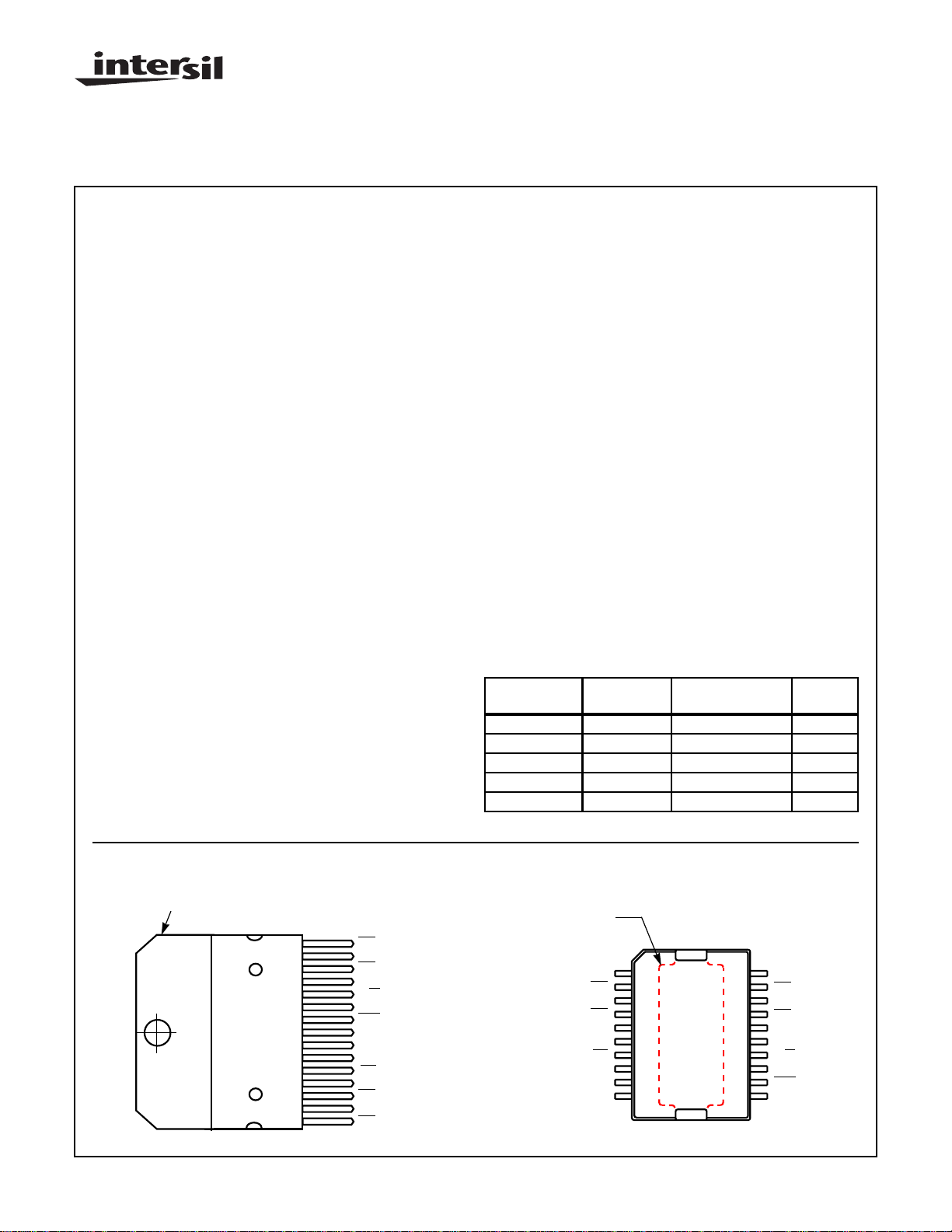
Pinouts
HIP0082, HIP0084 (SIP)
TOP VIEW
HEAT SINK TAB INTERNALLY CONNECTED
TO PIN 8 GROUND (V
CAUTION: These devices are sensitive to electrostatic discharge; follow proper IC Handling Procedures.
http://www.intersil.com or 407-727-9207
)
SS
15
14
13
12
11
10
9
8
7
6
5
4
3
2
1
| Copyright © Intersil Corporation 1999
IN3
OUT3
IN1
OUT1
W
R/
V
CC
RST
GND (V
TXD
CLK
CS
OUT2
IN2
OUT4
IN4
SS
)
1
HIP0082, HIP0084 (PSOP W/HEAT SLUG)
INTEGRAL COPPER
HEAT SINK ‘SLUG’
FOR PCB CONTACT
OR EXT. HEAT SINK
GND (SLUG)
GND (V
GND (SLUG)
IN4
OUT4
IN2
SS
OUT2
CS
CLK
TXD
)
TOP VIEW
1
2
3
4
5
6
7
8
9
10
20
GND (SLUG)
19
IN3
18
OUT3
17
IN1
16
15
14
13
12
11
GND (V
OUT1
R/
V
RST
GND (SLUG)
CC
)
SS
W
File Number 3643.4

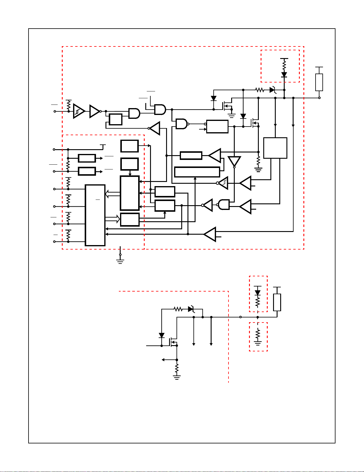
Block Diagram
V
CC
INx
V
CC
RST
TXD
CLK
CS
R/
W
RESET
POR
R/W
SHIFT
REG.
HIP0082, HIP0084
V
CC
V
R
SG
OL
D
OL
(NOTE 1)
1 OF 4
CHANNELS
RST
POR
S
Q
R
OSC
V
CC
POR
RST
OSC
OVER
TEMP.
DIAG.
REG.
WRITE/
STORE
FILTER
FILTER/
DELAY
DELAY
(SHORT CIRCUIT)
ISC REF (PROG. 3, 4)
Q
OL
CHARGE
PUMP
SC
(SHORT-TO-GND)
-
SG
V
+
REF
SG
OL
OL
Q
-
+
-
+
O
I
OL(MAX)
REF
I
OLF
REF
OL
OPEN-
LOAD
CURRENT
SENSE
BATT
LOAD
OUTx
V
SS
(GND)
HIP0084 OUTPUT STAGE
Q
O
SC
V
NOTE 2,
CASE 1
OUTx
NOTE 2,
CASE 2
SGOL
CC
V
BATT
LOAD
NOTES:
1. For Open-LoadDetection, the HIP0082 has an internal series pullup resistor, ROLand diode, DOLconnected fromOUTx to VCC.
2. HIP0084 OL (Open-Load) Detection:
Case 1: For OL Detection, an external series resistor and diode pullup connected from OUTx to VCC is needed.
Case 2: If no failure distinction for OL or SG (Short-to-GND) is required, both faults may be detected (without distinction), with an external
pulldown resistor.
For either case, the pullup or pulldown resistors should be typically 10kΩ or greater.
2

HIP0082, HIP0084
Absolute Maximum Ratings T
Supply Voltage (Logic and Control), VCC. . . . . . . . . . . . -0.3V to 7V
Power MOSFET Drain Voltage, VO (Note 3) . . . . . . -0.7 to V
Output Clamp Energy, EOK (See Note 5). . . . . . . . . . . . . . . . . 70mJ
Input Voltage (Logic and Driver Inputs), VIN. . . .-0.5V to VCC+0.5V
Maximum Output Current, Outputs 1 and 2 . . . . . . . . . . . . . . . . +2A
Maximum Output Current, Outputs 3 and 4 . . . . . . . . . . . . . . . . +5A
Maximum Total Output Current, All Outputs ON. . . . . . . . . . . . . +8A
Maximum Peak Output Current, I
Operating Conditions
Temperature Range . . . . . . . . . . . . . . . . . . . . . . . . . -40oC to 125oC
CAUTION: Stresses above those listed in “Absolute Maximum Ratings” may cause permanent damage to the device. This is a stress only rating and operation
of the device at these or any other conditions above those indicated in the operational sections of this specification is not implied.
= 25oC Thermal Information
A
Thermal Resistance (T ypical, Notes 5, 6, 7) θJA (oC/W) θJC (oC/W)
CLAMP
PowerSIP Package . . . . . . . . . . . . . . . 45 3
PSOP Package . . . . . . . . . . . . . . . . . . 40 2
Maximum Junction Temperature. . . . . . . . . . . . . . . -40oC to 150oC
Maximum Storage Temperature Range, T
Maximum Lead Temperature (During Soldering 10s) . . . . . . 300oC
(PSOP - Lead Tips Only)
, (Note 4) . . . . . -5A to I
O(MAX)
SC
Die Characteristics
Back Side Potential. . . . . . . . . . . . . . . . . . . . . . . .VSS (Tab Ground)
. . . . -55oC to 150oC
STG
NOTES:
3. The MOSFETOutput Drainis internally clamped with a Drain-to-Gate zenerdiode thatturns on the MOSFET to hold the Drain atthe
V
voltage. Refer to the Electrical Specifications Table for the V
CLAMP
CLAMP
voltage limits.
4. Each Output hasOverCurrent Shutdown protection inthe positive current direction.The maximumpeak current rating isset equalto the
minimum Over Current Shutdown as detailed in the Electrical Specification Table. In the event of an Over Current Shutdown the input
drive is latched OFF. The output short must be removed and the input toggled OFF and ON to restore the output drive.
5. Refer toApplication Note AN9416 for Single Pulse Energyand Device Dissipation rating information, including inductiveload operation
and other thermal stress characterization.
6. θJA is measured with the component mounted on an evaluation PC board in free air.
7. Maximum PSOP Package Dissipation at 125oC with 26oC/W Heat Sink (6 sq cm Copper PCB) is0.96W.
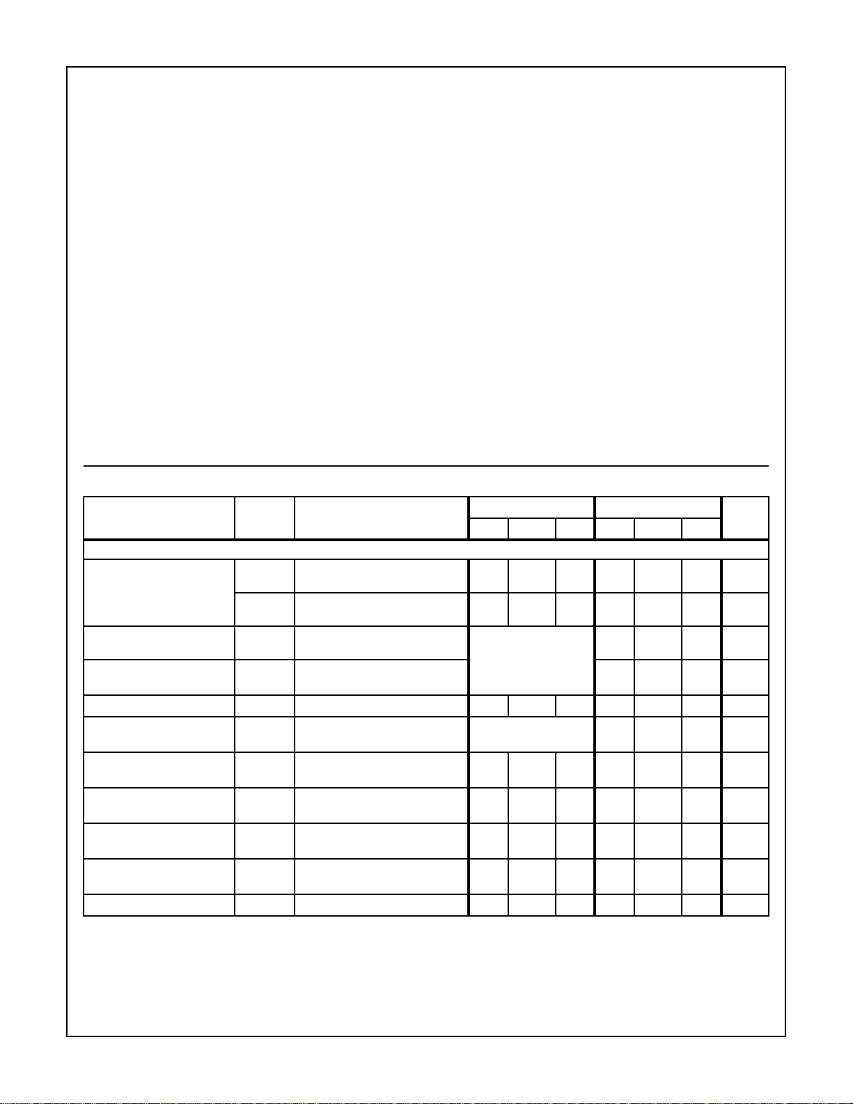
Electrical Specifications V
= 5V ±10%, TA = -40oC to 125oC; Unless Otherwise Specified
CC
HIP0082 HIP0084
PARAMETER SYMBOL TEST CONDITIONS
UNITSMIN TYP MAX MIN TYP MAX
POWER OUTPUTS
Output ON Resistance
(Normal Mode)
Output ON Resistance
(Normal Mode)
Output ON Resistance
(Normal Mode)
Output Zener Clamp Voltage V
Matching Zener Clamp
r
DS(ON)1
r
DS(ON)2
r
DS(ON)3,
r
DS(ON)4
r
DS(ON)1
r
DS(ON)2
r
DS(ON)3
r
DS(ON)4
Z
∆V
ZIOUT
,
Outputs 1 and 2, OneOutput ON,
I
= 2A, TJ = 150oC
OUT
Outputs 3 and 4, OneOutput ON,
I
= 2A, TJ = 150oC
OUT
,
Outputs 1 and 2, OneOutput ON,
I
= 2A, TJ = 75oC
OUT
,
Outputs 3 and 4, OneOutput ON,
I
= 2A, TJ = 105oC
OUT
I
= 40mA 73 80 90 73 80 90 V
OUT
- - 0.62
- - 0.57
N/A
- - 0.62 Ω
- - 0.57 Ω
- - 0.5 Ω
- - 0.5 Ω
= 40mA, tZ = 100µs N/A - - ±1.5 V
Voltage
Output Short Current Limit,
I
SC(L)
2 - 3.4 3 - 5.1 A
Outputs 1 and 2 (Note 8)
Output Short Current Limit,
I
SC(L)
ISC Bit High 2 - 3.4 2 - 3.4 A
Outputs 3 and 4 (Note 8)
Output Short Current Limit,
I
SC(H)
ISC Bit Low 5 - 7.5 5 - 8.3 A
Outputs 3 and 4 (Note 8)
Short Circuit Current Filter
t
SC
--1--3µs
Time
Output Capacitance C
V
O
= 16V, f = 1MHz - - 250 - - 250 pF
OUTX
3

HIP0082, HIP0084
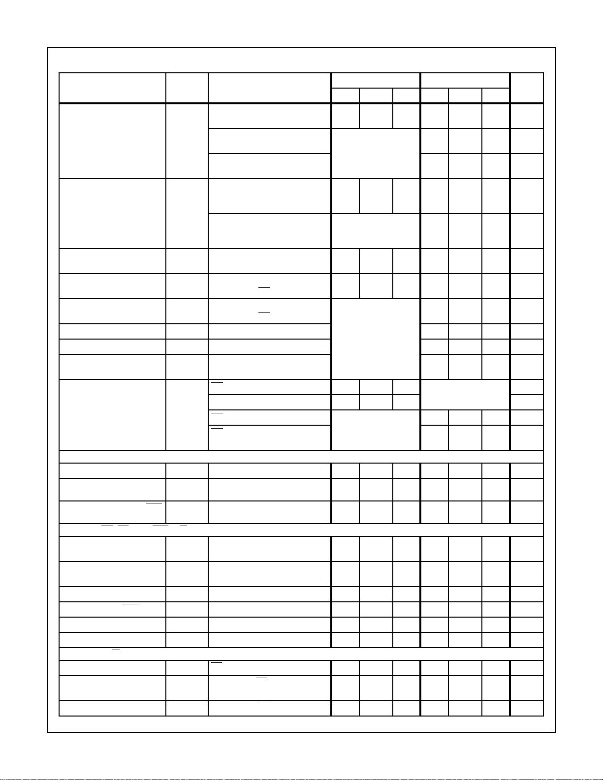
Electrical Specifications V
= 5V ±10%, TA = -40oC to 125oC; Unless Otherwise Specified (Continued)
CC
PARAMETER SYMBOL TEST CONDITIONS
Positive Output Voltage
Ramp Slew Rate, Inductive
Load Switching Off
SR1 I
= 1A, Load 6mH, 12Ω;
OUTX
Measure 25% to 75% of V
I
= 1A, Load 6mH, 12Ω;
OUTX
Measure 4V to 16V of V
I
= 1A, Load 6mH, 12Ω;
OUTX
Measure 75% to 95% of V
Negative Output Voltage
Ramp Slew Rate, Inductive
Load Switching On
SR2 V
= 12V, Load 6mH, 6Ω;
BATT
Measure 25% to 75%,
VCC = 5V ±2%
V
= 12V, Load 6mH, 6Ω;
BATT
Measure 25% to 75%,
TJ = 25oC, VCC = 5V ±2%
Output Negative Voltage
Ramp Fall Time
Turn-Off Delay t
t
I
f
OUTX
6Ω Load
d(OFF)IOUTX
= 2A, From 90% to 10%,
= 2A,
From 50% of INx to 10% of OUTx
Turn-On Delay t
d(ON)IOUTX
= 2A,
From 50% of INx to 90% of OUTx
Matching Turn-On Delay ∆t
Matching Turn-Off Delay ∆t
Output Rise Time t
d(ON)
d(OFF)
r
ForSR3Postive Ramp Conditions
From 10% to 90% of V
Output Leakage Current I
LK
INx = High, V
V
= 60V, VCC Open - - 10 µA
OUTX
INx = High, V
INx = Low, V
VCC = 0V
SUPPLY
Power Supply Current I
Low VCC Shutdown Thresh-
V
CC(LOW)
CC
Standby, No Load
(Note 9)
old
ActiveSupply Range for RST
V
CC(RST)
Pin
INPUTS (INx, CS, CLK, RST, R/W, TXD)
Low-Level Input Voltage V
High-Level Input Voltage V
Input Hysteresis Voltage V
Reset Time after RST L→Ht
Input Pull-Up Resistance R
Input Current
IL
IH
HYS
RST
IN
Logic High Input Voltage
I
IH
TXD PIN (R/W = High)
Three-State Leakage Current
I
Logic High Output Voltage V
Logic Low Output Voltage V
LK_TXD
TXDHIOH
CS = High, V
TXDLIOL
= -4mA, CS = Low
= 3.2mA, CS = Low
HIP0082 HIP0084
6 70 100 6 14 24 V/µs
Z
N/A 2 9 20 V/µs
Z
5.1 11 20.4 V/µs
Z
0.75 15 25 0.75 1.5 3.75 V/µs
N/A 1 - 3 V/µs
- - 25 - 15 25 µs
0.5 - 3 - - 10 µs
N/A - - 10 µs
--±3 µs
--±3 µs
-10µs
Z
= 60V - - 10 N/A µA
OUTX
OUTX=VCC+
= 0V to 60V,
OUTX
to 60V N/A -10 - 10 µA
-10 - 10 µA
- 7.5 15 - 7.5 15 mA
3.4 3.7 4.0 3.4 3.7 4.0 V
3.5 - 5.5 3.5 - 5.5 V
-0.3 - 0.2 X
0.7 x
V
CC
-VCC+
-0.3 - 0.2 X
V
CC
0.7 x
0.3
V
CC
-VCC+
0.85 1.2 2.25 0.85 1.2 2.25 V
48-8048-80µs
50 - 150 50 - 150 kΩ
--2--2µA
TXD
= V
CC
-5 - 5 -5 - 5 µA
VCC -
0.4
--VCC -
0.4
--V
- - 0.42 - - 0.42 V
V
UNITSMIN TYP MAX MIN TYP MAX
V
CC
V
0.3
4
 Loading...