Intersil Corporation HIP0081, HIP0080 Datasheet
HIP0080, HIP0081
September 1998 File Number 3018.4
Quad Inverting Power Drivers with Serial
Diagnostic Interface
HIP0080, HIP0081The HIP0080/0081 Quad Power Drivers
contain four individually protected NDMOS power output
transistor switches to drive inductive and resistive loads
such as: relays, solenoids, injectors, AC and DC motors,
heaters and incandescent lamp displays. The 4 Power
Drivers are low-side switches driven by CMOS logic input
control stages. Each Output Power Driver is protected
against over-current, over-temperature and over-voltage.
An internal drain-to-gatezener diode provides the clamping
protection for over-voltage. Diagnostic circuits provide
ground short,supply short, open load and thermal overload
detection for each of the 4 output stages. Each of the 4
input drivers and their respective diagnostic filters are
controlled by one ENABLE input.
HIP0080, HIP0081The inputs are CMOS logic compatible
and individually control the output drivers with an active
high state for turn-on. All other control inputs are active
high with the exception of the Chip Select (
active low. The DATAIN (DI) and DATAOUT (DO) are
positive logic and the Clock (CLK) input for the Serial
Interface is active on the rising edge of the CLK pulse. All
Inputs except the HIP0080 ENABLE have a nominal level
of hysteresis. IN1, IN2, IN3, IN4 and ENABLE have pulldown resistors of approximately 100kΩ. This switches off
any channel that has an unterminated input.
HIP0080, HIP0081Filters are used on the outputs of the
fault sensing comparators to avoid the detection of short
duration transient spikes. The on-chip oscillator is used to
clock an internal shift register in each filter. If the fault
condition is longer than a preset number of clock cycles,
the fault condition is recognized and the respective bit is
set in the diagnostic register. No filter is used in the
thermal-overload feedback circuit and the bit is set when
thermal shutdown occurs.
CS) which is
Features
• Low Side Power MOSFET Output Drivers
• Output Driver Protection
- Over-Current Shutdown
- Over-Temperature Shutdown with Hysteresis
- Over-Voltage Internal Clamp
• HIP0081 Output Current Switching Capability:
- Each Output, I
- All Outputs ON, Equal I
- All Outputs ON, Equal I
• HIP0080 Output Current Switching Capability:
- Each Output, I
- All Outputs ON, Unequal I
- All Outputs ON, Unequal I
• HIP0080 - Low Idle Current Shutdown Mode
• Regulated Interface for 5V CMOS Logic Inputs
• Open Drain High Z DATAOUT
• Fault Mode Output for Shorts, Opens and Over-Temperature
• 16-Bit Serial Diagnostic Register
• SPI Bus Compatible Data Readout
• HIP0081 - Low θ
o
C to 125oC Operating Temperature Range
• -40
. . . . . . . . . . . . . . . . . . . . . . 2.2A DC
OUT
. . . . . . . . . . . . . . . . 6A DC
OUT
. . . . . . . . . . 8A PK, 500ms
OUT
. . . . . . . . . . . . . . . . . . . . . . 1.3A DC
OUT
. . . . . . . . . . . . . . 3A DC
OUT
. . . . . . . . 4A PK, 500ms
OUT
Power Package. . . . . . . . . . . . 3oC/W
JC
Applications
• Drivers For: • System Use:
- Solenoids - Injectors - Automotive
- Relays - Steppers - Appliances
- Power Output - Motors - Industrial
- Lamps - Displays - Robotics
HIP0080, HIP0081For normal operating conditions, a
Reset turns off all outputs when the V
3.5V. The inter nal bandgap and bias supply function
includes a 5V regulated supply for the low voltage signal
and logic circuits.
1
level drops below
CC
CAUTION: These devices are sensitive to electrostatic discharge; follow proper IC Handling Procedures.
Ordering Information
TEMP.
PART NUMBER
HIP0081AS1 -40 to 125 15 Ld SIP Z15.05A
HIP0081AS2 -40 to 125 15 Ld SIP Z15.05B
HIP0080AM -40 to 125 28 Ld PLCC N28.45
http://www.intersil.com or 407-727-9207
RANGE (oC) PACKAGE
| Copyright © Intersil Corporation 1999
PKG.
NO.
HIP0080, HIP0081
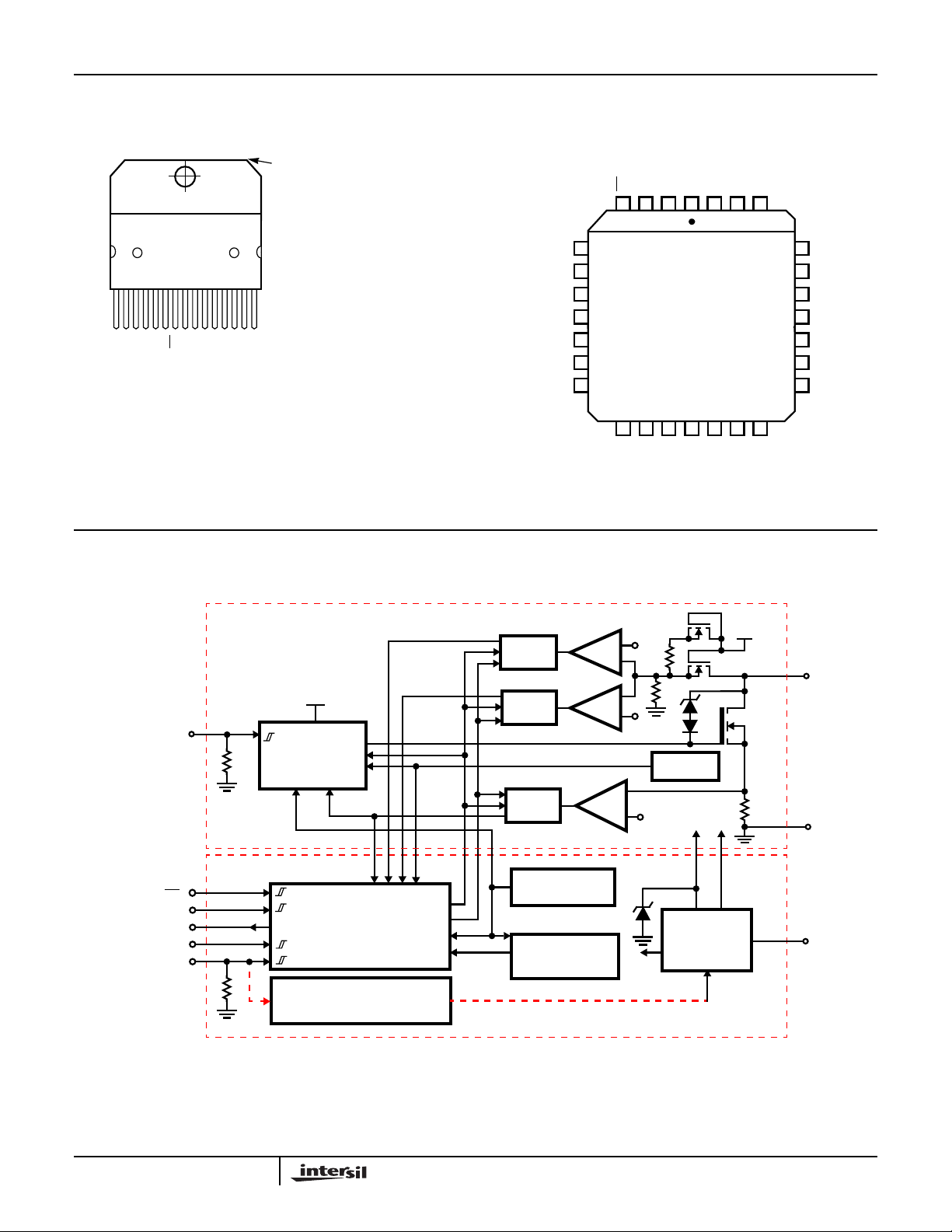
Pinouts
HIP0081 (SIP)
TOP VIEW
HEAT SINK TAB AT SAME
POTENTIAL AS PIN 8-GND
IN1
OUT1
DATAOUT
IN2
CLK
OUT2
CS
10
987654321
GND
ENABLE
CC
V
IN3
OUT3
DATAIN
IN4
1514131211
OUT4
Functional Block Diagram
GND
GND
GND
GND
GND
GND
GND
HIP0080 (PLCC)
TOP VIEW
CS
CLK
5
6
7
8
9
10
11
12 13 14 15 16 17 18
CC
V
ENABLE
OUT 2
1234
OUT 3
IN 2
IN 3
DAT A
OUT
DATAIN
IN1
IN 4
OUT 1
262728
OUT 4
GND
25
GND
24
GND
23
GND
22
GND
21
GND
20
GND
19
IN1
CS
CLK
DATAOUT
DATAIN
ENABLE
1 OF 4 SWITCH/CHANNELS
VCC1
100kΩ
DR1-CNTL
POR
SC
CONTROL AND 16-BIT
DIAGNOSTIC SHIFT
DO
REGISTER
(NOTE)
LOW IDLE CURRENT
POWER DOWN SWITCH
(HIP0080 ONLY)
100kΩ
DR
EN
TS
EN
FCLK
O.L.
FILTER
G.S.
FILTER
S.C.
FILTER
POR
(PWR-ON-RST)
500kHz OSC
(FILTER-FCLK)
COMP
COMP
COMP
O.L.
V
REF
V
REF
G.S.
10kΩ
VREF
I
LIMIT
10kΩ
74V
TEMP.
SENSE
SC
VCC1
14V
BANDGAP
REF. AND BIAS
VOLTAGE
SOURCES
VCC1
0.01Ω
OUT1
GND
V
CC
NOTE: HIP0080 - No enable hysteresis.
2
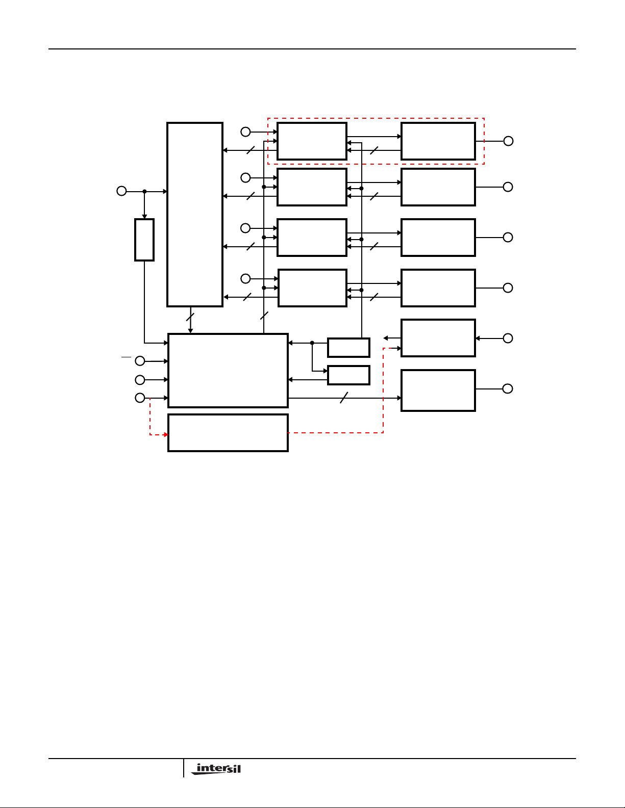
Functional Signal Flow Diagram
DATAIN (DI)
TEST
CS
CLK
ENABLE (EN)
SHIFT REGISTER
4
CONTROL
HIP0080, HIP0081
1 OF 4 SWITCH/CHANNELS (SEE FUNCTIONAL BLOCK DIAGRAM)
IN1
DR OUT1
DR OUT2
DR OUT3
DR OUT4
BANDGAP
AND BIAS
DATAOUT
(DRIVER)
IN2
IN3
IN4
DR1 CNTL
4
4
4
4
4
(DATAPATH)
4
DR2 CNTL
(DATAPATH)
4
DR3 CNTL
(DATAPATH)
4
DR4 CNTL
(DATAPATH)
4
POR
OSC
3
(DRVR)
(DRVR)
(DRVR)
(DRVR)
SERIAL
OUT1
OUT2
OUT3
OUT4
V
CC
DATAOUT
(DO)
LOW IDLE CURRENT
POWER DOWN SWITCH
(HIP0080 ONLY)
3
HIP0080, HIP0081
Absolute Maximum Ratings Thermal Information
Supply Voltage (Logic and Control), VCC. . . . . . . . . . . . -16 to 45V
Power MOSFET Drain Voltage, VO (Note 1) . . . . . . -0.5 to V
Maximum Output Clamp Energy, EOK (HIP0080) . . . . . . . . .
Maximum Output Clamp Energy, EOK (HIP0081) . . . . . . . . .
CLAMP
Note 4
Note 4
Input Voltage (Logic and Driver Inputs), VIN . . . . . . . . . . . -0.5 to 7V
Output Voltage, DATAOUT . . . . . . . . . . . . . . . . . . . . . . . . -0.5 to 7V
HIP0080 Output Current
Each Output, I
Each Output, I
Total of 4 Outputs ON, Unequal I
OUT(PEAK)
OUT(DC)
Total of 4 Outputs ON, Unequal I
HIP0081 Output Current
Each Output, I
Each Output, I
Total of 4 Outputs, ON, Unequal I
OUT(PEAK)
OUT(DC)
Total of 4 Outputs ON, Unequal I
, (Note 2) . . . . . . -1.5A to I
OUT(SC)
. . . . . . . . . . . . . . . . . . . . . . . . +1.3A
. . . . . . . . . . . . . . . . +3A
OUT
. . . . . +4A/500ms (Max)
OUT
, (Note 2) . . . . . . . . . -2 to I
OUT(SC)
. . . . . . . . . . . . . . . . . . . . . . . . +2.2A
. . . . . . . . . . . . . . . +6A
OUT
. . . . . +8A/500ms (Max)
OUT
Operating Conditions
Ambient Temperature Range . . . . . . . . . . . . . . . . . -40oC to 125oC
Junction Temperature Range . . . . . . . . . . . . . . . . . -40oC to 150oC
CAUTION: Stresses above those listed in “Absolute Maximum Ratings” may cause permanent damage to the device. This is a stress only rating and operationofthe
device at these or any other conditions above those indicated in the operational sections of this specification is not implied.
NOTES:
1. The MOSFET Output Drainis internally Clamped with a Drain-to-Gate zenerdiode that turns-on the MOSFET to holdthe Drain at the V
voltage. Refer to the Electrical Characteristic Tables for the V
2. Each Output has Over-Current Shutdown protection in the positive current direction. The maximum peak current rating is determined by the
minimum Over-Current Shutdown as detailed in the Electrical Specification Table. In the event of an Over-Current Shutdown the input drive is
latched OFF. The output short must be removed and the input toggled OFF and ON to restore the output drive.
3. Effective HeatSinking forthe HIP0080 PLCC packagerequires a PC Boardsoldermount or equivalent.TheHIP0080 θJAjunction-to-air thermal
resistance is given for a PC Board with 2 sq. in. of 1 oz. surface mount ground copper extending away from the package. For additional Power
Dissipation Derating information, see Figure 8 curves.
4. Refer to Figures 4 and 5 Single Pulse Output Clamp Energy vs. Time Capability of the HIP0080 and HIP0081. The safe margin for single pulse
energy operation is below the dotted line shown in Figures 4 and 5.
CLAMP
Thermal Resistance (Typical, Note 3) θJA(oC/W) θJC(oC/W)
HIP0080. . . . . . . . . . . . . . . . . . . . . . . . 43 N/A
HIP0080 (on 2 sq. in. PC Board) . . . . . 33 N/A
HIP0081. . . . . . . . . . . . . . . . . . . . . . . . 45 3
HIP0080 Power Dissipation with a 2 sq. in. PC board heat sink:
At 85oC . . . . . . . . . . . . . . . . . . . . . . . . . . . . . . . . . . . . . . . .1.95W
Above 85oC:. . . . . . . . . . . . . . . . . . . Derate Linearly at 30mW/oC
HIP0081 Power Dissipation with infinite heat sink:
At 125oC . . . . . . . . . . . . . . . . . . . . . . . . . . . . . . . . . . . . . . 8.33W
Above 125oC . . . . . . . . . . . . . . . . .Derate Linearly at 333 mW/oC
Maximum Storage Temperature Range, T
Maximum Lead Temperature (Soldering 10s) . . . . . . . . . . . 300oC
. . . . -55oC to 150oC
STG
Die Characteristics
HIP0080 Back Side Potential . . . . . . . . . . . . . . Frame, GND Leads
HIP0081 Back Side Potential . . . . . . . . . Heat Sink Tab, GND Lead
voltage limits.
CLAMP
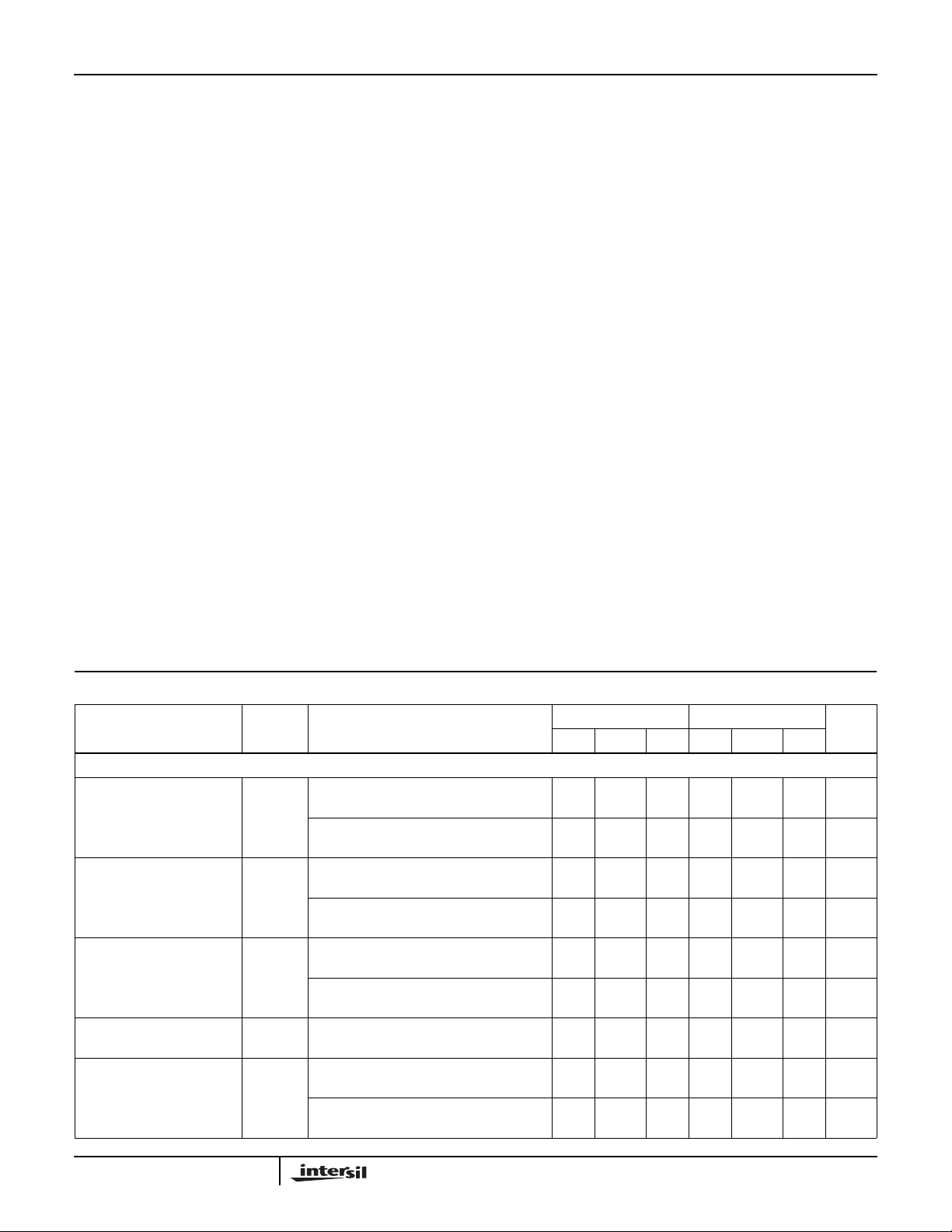
Electrical Specifications V
= 5.5V to 25V ±5%, TA = -40oC to 125oC, Unless Otherwise Specified
CC
PARAMETER SYMBOL TEST CONDITIONS
POWER OUTPUTS
Output ON Resistance
(HIP0081)
Output ON Resistance
(HIP0080)
HIP0081 Output Off Current I
r
r
OFF
VCC = 10 to 25V, All Outputs ON
ON
I
= I
OUT1
V
I
OUT1
VCC = 10 to 25V, All Outputs ON
ON
I
OUT1
V
I
OUT1
OUT2
= 5.5 to 10V, All Outputs ON
CC
= I
OUT2
= I
OUT2
= 5.5 to 10V, All Outputs ON
CC
= I
OUT2
Inputs Low, Each V
TA = 25oC to 125oC
Inputs Low, Each V
TA = -40oC
HIP0081 Output Leakage
Current
HIP0080 Output Off
Current
I
OFFLK
I
OFF
Inputs Low, Each V
VCC = 0V
Inputs Low, Each V
ENABLE High, TA= 25oC to 125oC
Inputs Low, Each V
ENABLE High, TA = -40oC
= I
= I
= I
= I
OUT3
OUT3
OUT3
OUT3
OUT
OUT
OUT
OUT
OUT
= I
= I
= I
= I
= 60V
= 60V,
= 60V,
= 25V,
= 25V,
OUT4
OUT4
OUT4
OUT4
HIP0080 HIP0081
UNITSMIN TYP MAX MIN TYP MAX
-----0.5Ω
= 1A
-----1.0Ω
= 0.7A
- - 1.0 - - - Ω
= 0.5A
- - 2.0 - - - Ω
= 0.4A
- - - - 0.75 1.0 mA
- - - - 0.75 1.5 mA
- - - - 1.0 10 µA
- 0.75 1.0 - - - mA
- 0.75 1.5 - - - mA
4
HIP0080, HIP0081
Electrical Specifications V
= 5.5V to 25V ±5%, TA = -40oC to 125oC, Unless Otherwise Specified (Continued)
CC
HIP0080 HIP0081
PARAMETER SYMBOL TEST CONDITIONS
HIP0080 Output Leakage
Current
Over-Voltage Clamp Range V
Current Short Circuit Prot. I
Short Circuit Det. Delay t
Output ON-OFF Voltage
I
OFFLK
CLAMP
OUT(SC)
SCDLY
Inputs Low, Each V
ENABLE Low
IN Inputs Low (Outputs OFF),
I
= 40mA
OUT
OUT
= 25V,
- 1.0 10 - - - µA
27-4373-89V
Note 2 1.3 - 3 2.2 - 4.8 A
-6--6-µs
Resistive Load - 10 - - 10 - V/µs
Ramp Rate
Turn-On Delay t
Turn-Off Delay t
PHL
PLH
VCC = 14V, R
VCC = 14V, R
= 14Ω --8--8µs
LOAD
= 14Ω --8--8µs
LOAD
SUPPLY
Power Supply Current I
Power Supply Reset Active V
Shut-Down Current Mode I
CC
CC_RSTTA
T
SHTDN
Enable Low - 130 200 - - - µA
= 25oC to TA = 125oC 3-43-4V
= -40oC 2.7 - 4 2.7 - 4 V
A
- 20 30 - 20 30 mA
INPUTS
Low-Level Input Voltage V
High-Level Input Voltage V
Input Hysteresis Threshold V
IN_HYS
Input Pull-Down
IL
IH
(N.A. to HIP0080 ENABLE) 0.85 - 2.25 0.85 - 2.25 V
R
IN1, IN2, IN3, IN4 and ENABLE 50 100 200 50 100 200 kΩ
PD
--1--1V
3.5 - - 3.5 - - V
Resistance
DATAOUT (Open Drain)
Leakage Current I
DO_LEAKVDO
Logic Low Output Voltage V
Max. Logic Low Current I
Oscillator Frequency f
Serial Interface Clock Freq. f
OLIDO
OH
OSC
CLK
= 7V, DO OFF (High) - - 10 - - 10 µA
= 1.6mA, DO ON (Low) - - 0.4 - - 0.4 V
VDO = 4.5V, DO ON 1.6 - - 1.6 - - mA
- 500 - - 500 - kHz
Note 5 - - 2 - - 2 MHz
DIAGNOSTIC AND PROTECTION
Over-Temperature
150 165 - 150 165 -
Shutdown Threshold
Shutdown Temperature Hys-
-15--15-
teresis
Output Short-to-GND
Threshold
Short-to-GND Hysteresis V
Open-Load Resistance for
V
= 5.5V to 16V - 0.24x
CC
= 5.5V to 16V - 0.02x
CC
= 5.5V to 16V 5 - 25 5 - 25 kΩ
V
CC
V
CC
V
CC
- - 0.24x
V
CC
- - 0.02x
V
CC
No-Load Warning
Filter Delay Time for O.L. or
-12--12-µs
Short-to-GND
NOTE:
5. The maximum Serial Clock Frequency may be limited by the time constant of the external load network at the DATAOUT pin.
UNITSMIN TYP MAX MIN TYP MAX
o
C
o
C
-V
-V
5
 Loading...