December 1997
HIP0061
60V, 3.5A, 3-Transistor Common Source
ESD Protected Power MOSFET Array
Features
• Three 3.5A Power MOS N-Channel Transistors
• Output Voltage to 60V
•r
DS(ON)
. . . . . 0.225Ω Max Per Transistor at VGS= 10V
• Pulsed Current. . . . . . . . . . . . . . . .10A Each Transistor
• Avalanche Energy . . . . . . . . . . 100mJ Each Transistor
• Grounded Tab Eliminates Heat Sink Isolation
Applications
• Automotive
• Appliance
• Industrial Control
• Robotics
• Relay, Solenoid, Lamp Drivers
Ordering Information
TEMP.
PART NUMBER
HIP0061AS1 -40 to 125 7 Ld Staggered
RANGE (oC) PACKAGE
Vertical SIP
PKG.
NO.
Z7.05C
Description
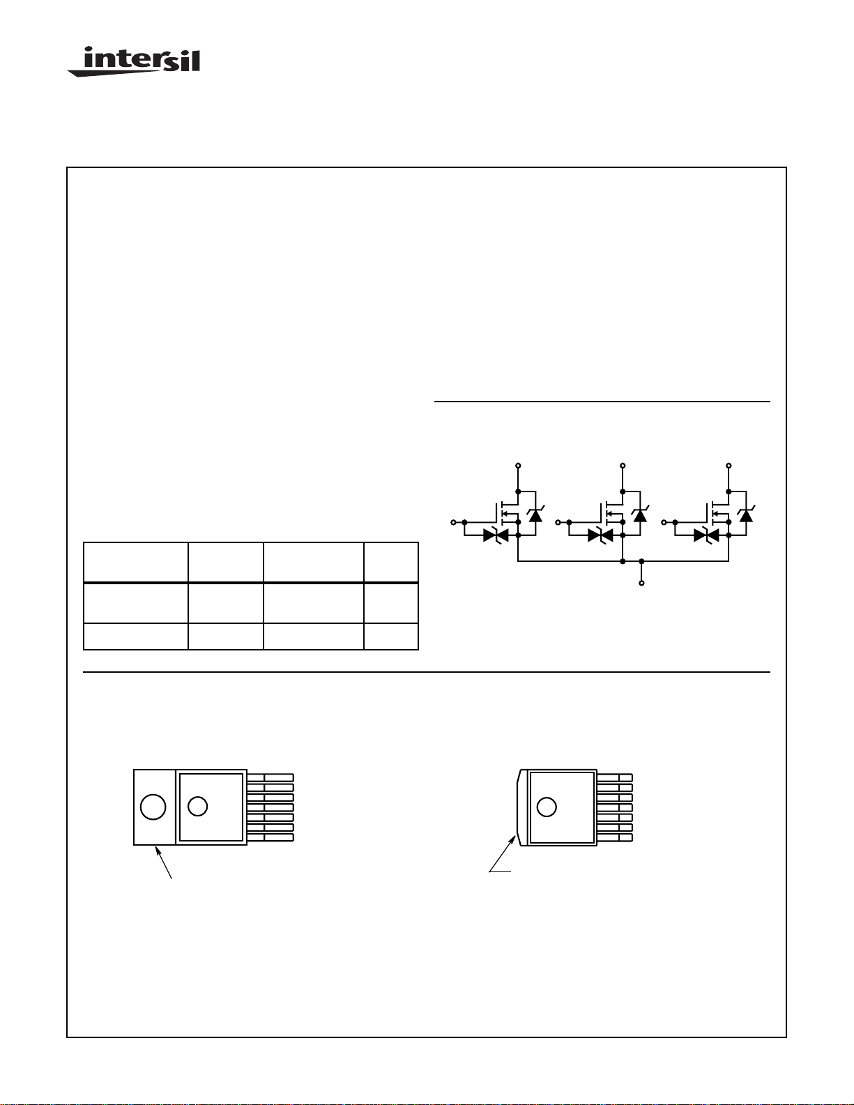
The HIP0061 is a power MOSFET array that consists of
three matched N-Channel enhancement mode MOS transistors connected in a common source configuration. The
advanced Harris PASIC2 process technology used in this
product utilizes efficient geometries that provides outstanding device performance and ruggedness.
The HIP0061 is designed to integrate three power de vices in
one chip thus providing board layout area and heat sink savings for applications such as Motor Controls, Lamps,
Solenoids and Resistive Loads.
Symbol
DRAIN3
7
GATE1
1
DRAIN1
2
GATE2
3
DRAIN2
5
GATE3
6
4
SOURCE, TAB
HIP0061AS2 -40 to 125 7 Ld Gullwing SIP Z7.05B
Pinouts
HIP0061AS1
(SIP - VERTICAL)
TOP VIEW
7 DRAIN3
6 GATE3
5 DRAIN2
4 SOURCE
3 GATE2
2 DRAIN1
1 GATE 1
TAB
TAB (SOURCE) INTERNALLY CONNECTED TO PIN 4
HIP0061AS2
(SIP - GULLWING)
TOP VIEW
7 DRAIN3
6 GATE3
5 DRAIN2
4 SOURCE
3 GATE2
2 DRAIN1
1 GATE 1
TAB
TAB (SOURCE) INTERNALLY CONNECTED TO PIN 4
CAUTION: These devices are sensitive to electrostatic discharge; follow proper IC Handling Procedures.
http://www.intersil.com or 407-727-9207
| Copyright © Intersil Corporation 1999
1
File Number 3982.3

HIP0061
Absolute Maximum Ratings T
Drain to Source Voltage, V
(Over Operating Junction and Case Temperature Range) . . . . 60V
Drain to Gate Voltage, V
Gate to Source Voltage, VGS . . . . . . . . . . . . . . . . . . . . . . .-15, +20V
Pulsed Drain Current, IDM, Each Output,
All Outputs on at VGS = 10V (Notes 1, 2). . . . . . . . . . . . . . . . 10A
Continuous Source to Drain Diode Current, I
at VGS= 10V (Note 2) . . . . . . . . . . . . . . . . . . . . . . . . . . . . . .3.5A
Continuous Drain Current, IDS, Each Output,
All Outputs on at VGS = 10V (Note 2) . . . . . . . . . . . . . . . . . .3.5A
DS
. . . . . . . . . . . . . . . . . . . . . . . . . . . 60V
DGR
=25oC Thermal Information
A
Thermal Resistance (Typical, Note 4) θJA (oC/W) θJC (oC/W)
SIP-Vertical Package . . . . . . . . . . . . . 55 3
SIP-Gullwing Package . . . . . . . . . . . . 55 3
Maximum Junction Temperature, TJ. . . . . . . . . . . . . . . . . . . . 150oC
Maximum Storage Temperature Range, T
Maximum Lead Temperature (Soldering 10s). . . . . . . . . . . . 300oC
SD
Die Characteristics
Back Side Potential. . . . . . . . . . . . . . . . . . . . . . . . . V- (Source, Tab)
. . . . -55oC to 150oC
STG
Single Pulse Avalanche Energy, EAS(Note 3) . . . . . . . . . . . . 100mJ
Operating Conditions
Temperature Range . . . . . . . . . . . . . . . . . . . . . . . . . -40oC to 125oC
Drain to Source On-State Voltage Range . . . . . . . . . . . . 5V to 10V
CAUTION: Stresses above those listed in “Absolute Maximum Ratings” may cause permanent damage to the device. This is a stress only rating and operation
of the device at these or any other conditions above those indicated in the operational sections of this specification is not implied.
NOTES:
1. Pulse width limited by maximum junction temperature.
2. Drain current limited by package construction.
3. VDD = 25V, Start TJ = 25oC, L = 15mH, RGS = 50Ω, I
4. θJA is measured with the component mounted on an evaluation PC board in free air.
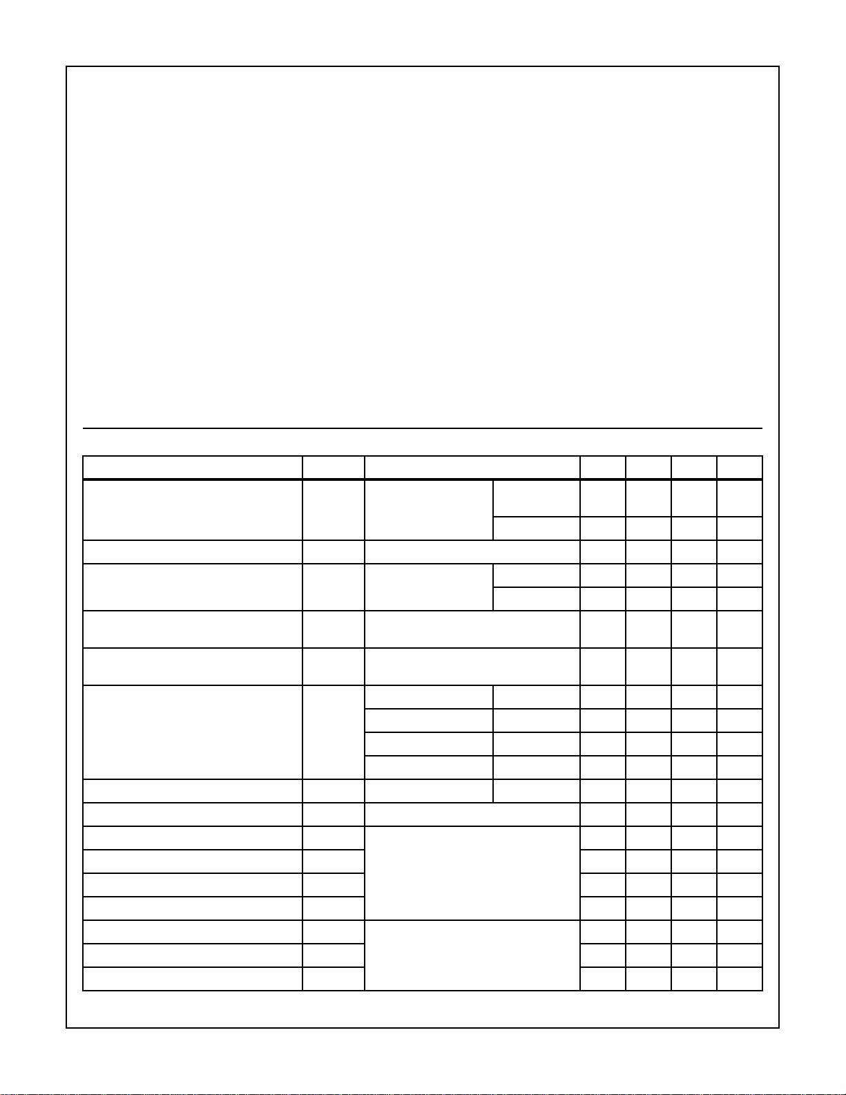
Electrical Specifications T
= 25oC, Unless Otherwise Specified
C
PARAMETERS SYMBOL TEST CONDITIONS MIN TYP MAX UNITS
Drain to Source Breakdown Voltage BV
Gate Threshold Voltage V
Zero Gate Voltage Drain Current I
Forward Gate Current, Drain Short
DSSID
GS(TH)VGS
DSS
I
GSSF
Circuited to Source
Reverse Gate Current, Drain Short
I
GSSR
Circuited to Source
Drain to Source On Resistance (Note 5) r
Drain to Source On Resistance Matching r
Forward Transconductance (Note 5) g
Turn-On Delay Time (Note 6) t
Rise Time (Note 6) t
Turn-Off Delay Time (Note 6) t
Fall Time (Note 6) t
Total Gate Charge (Note 6) Q
Gate-Source Charge (Note 6) Q
Gate-Drain Charge (Note 6) Q
DS(ON)VGS
DS(ON)VGS
fs
d(ON)
r
d(OFF)
f
g(TOT)VDS
gs
gd
= 3.5A. See Figures 1, 2, 12, and 13.
PEAK
= 100µA, VGS = 0V TC = -40oC to
60 - - V
125oC
TC = 25oC-70-V
= VDS, ID = 250µA 1.8 2.3 2.7 V
VDS = 60V
VGS = 0V
TC = 25oC--1µA
TC = 125oC--10µA
VDS = 0V, VGS = 20V - - 100 nA
VDS = 0V, VGS = -15V - - -100 nA
= 10V, ID = 3.5A TC = 25oC - 0.215 0.265 Ω
VGS = 10V, ID = 3.5A TC = 125oC - 0.365 0.425 Ω
VGS = 5V, ID = 2A TC = 25oC - 0.275 0.320 Ω
VGS = 5V, ID = 2A TC = 125oC - 0.465 0.5 Ω
= 10V, ID = 3.5A TC = 25oC-95-%
VDS = 10V, ID = 1A - 2.5 - S
VDD = 30V, RL = 15Ω,
VGS = +10V, ID = 2A, RG = 50Ω
See Figure 14
-10 -ns
-25 -ns
-18 -ns
-12-ns
= 50V, VGS = 10V, ID = 2A
See Figures 16, 17
- 8.0 9.5 nC
- 0.7 1.0 nC
- 3.5 4.0 nC
2

HIP0061
Electrical Specifications T
= 25oC, Unless Otherwise Specified (Continued)
C
PARAMETERS SYMBOL TEST CONDITIONS MIN TYP MAX UNITS
Short-Circuit Input Capacitance,
Common Source
Short-Circuit Output Capacitance,
C
C
ISS
OSS
VDS = 25V, VGS = 0V
f = 1MHz
Common Source
Short-Circuit Reverse Transfer
C
RSS
Capacitance, Common Source
Source-Drain Diode Ratings and Specifications
PARAMETERS SYMBOL TEST CONDITIONS MIN TYP MAX UNITS
Diode Forward Voltage (Note 5) V
Reverse Recovery Time t
SD
rr
ISD = 2A, VGS = 0V - 0.9 1.1 V
ISD = 2A, dISD/dt = 100A/µs -50 -ns
NOTES:
5. Pulse test: Pulse width ≤ 300µs, duty cycle ≤ 2%.
6. Independent of operating temperature.
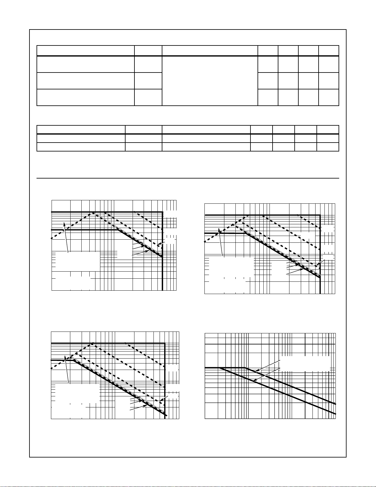
Typical Performance Curves
10
10µs
- 142 - pF
- 107 - pF
-24 -pF
10
10ms
1
OPERATION IN THIS
AREA MAY BE
LIMITED BY r
, DRAIN CURRENT (A)
D
I
TC = 25oC
TJ = MAX RATED
0.1
1
DS(ON)
V
, DRAIN VOLTAGE (V)
DS
100ms
DC
10
FIGURE 1A. 25oC SAFE-OPERATING AREA CURVE
10
1
OPERATION IN THIS
AREA MAY BE
LIMITED BY r
, DRAIN CURRENT (A)
D
I
TC = 125oC
= MAX RATED
T
J
0.1
1
FIGURE 1C. 125
DS(ON)
, DRAIN TO SOURCE VOLTAGE (V)
V
DS
o
C SAFE-OPERATING AREA CURVE FIGURE 2. UNCLAMPED INDUCTIVE-SWITCHING
10ms
100ms
DC
10
100µs
1ms
10µs
100µs
1ms
100
100
1
OPERATION IN THIS
AREA MAY BE
, DRAIN CURRENT (A)
D
I
0.1
LIMITED BY r
TC = 105oC
T
= MAX RATED
J
1
DS(ON)
, DRAIN TO SOURCE VOLTAGE (V)
V
DS
FIGURE 1B. 105
50
10
5
, AVALANCHE CURRENT (A)
AS
I
1
0.001
tAV, TIME IN AVALANCHE (ms)
100µs
10ms
100ms
DC
10 100
o
C SAFE-OPERATING AREA CURVE
STARTING T
STARTING TJ = 125oC
0.01 1.00.1
= 25oC
J
10µs
100µs
1ms
3
 Loading...