Intersil Corporation HIP0051 Datasheet

June 1996
HIP0051
0.25A/50V Octal Low Side Power Driver
with Serial Bus Control
Features
• Eight Open Drain - NDMOS Low Side Drivers Each
Capable of 250mA
• High V olta ge P o wer BiMOS with Low Idle and Standb y
Current
• Over-Voltage Clamp Protection
- Each Output . . . . . . . . . . . . . . . . . . . . . . . 50V Typical
• Serial Data Input, Parallel Output Power Drive
• Common Enable for Output Drivers and Data Storage
Register
o
• -40
C to 85oC Operating Range
Applications
• Automotive and Industrial Systems
• Solenoids, Relays and Lamp Drivers
• Logic and µP Controlled Drivers
• Robotic Controls
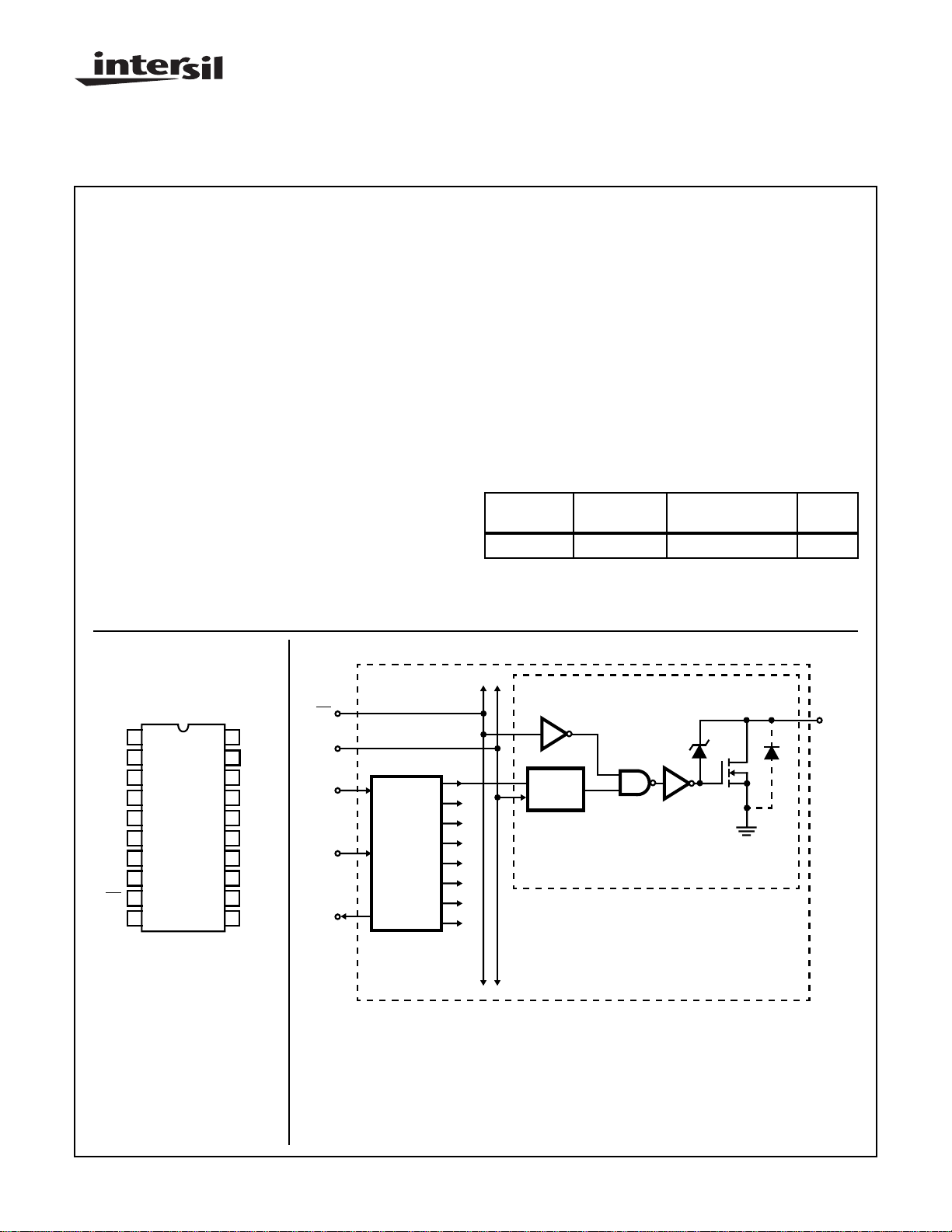
Pinout
Block Diagram
Description
The HIP0051 is a logic controlled, eight channel Octal Low
Side Power Driver. As shown in the Block Diagram, the
outputs are controlled via the serial data interface which
allows the data to be shifted out, allowing control of other
cascaded serial devices.
The HIP0051 is fabricated in a Power BiMOS IC process,
and is intended for use in automotive and other applications
having a wide range of temperature and electrical stress
conditions. It is particularly suited for driving lamps, displays,
relays, and solenoids in applications where low operating
power, high breakdown voltage, and high output current at
high temperature is required.
Ordering Information
PART
NUMBER
HIP0051IB -40 to 85 20 Ld SOIC M20.3
TEMP.
RANGE (oC) PACKAGE
PKG.
NO.
GND
V
CC
DR0
DR1
DR2
DR3
NC
EN
GND
SI
1
2
3
4
5
6
7
8
9
10
HIP0051
(SOIC)
TOP VIEW
20
19
18
17
16
15
14
13
12
11
GND
LGND
SO
DR7
DR6
DR5
DR4
SCK
STR
GND
EN
STR
SCK
SO
OUTPUT DRIVER
(ENABLE)
(STROBE)
SI
8-BIT
SERIAL
(SPI)
INPUT
REGISTER
(DATA IS
PARALLEL
OUTPUT
LATCHED
WHEN
STROBED)
Q0
Q1
Q2
Q3
Q4
Q5
Q6
Q7
OUTPUT
LATCH
(CHANNEL 1 OF 8)
DR#0
CAUTION: These devices are sensitive to electrostatic discharge; follow proper IC Handling Procedures.
http://www.intersil.com or 407-727-9207
| Copyright © Intersil Corporation 1999
1
File Number 4155

Specifications HIP0051
Absolute Maximum Ratings Thermal Information
Output Voltage, V
Input Voltage, VIN . . . . . . . . . . . . . . . . . . . . . . -0.3V to VCC+ 0.3V
Logic Supply Voltage, VCC. . . . . . . . . . . . . . . . . . . . . . -0.3V to +7V
Output Clamp Energy, 25oC (5ms Pulse). . . . . . . . . . . . . . . . . 75mJ
Continuous Output Load Current, I
Continuous Output Current, I
Peak Output Current
Each Output, Other Outputs OFF . . . . . . . . . . . . . . . . . . . . . ±2A
Peak Avalanche Current (3ms duration). . . . . . . . . . . . . . . . . . 1A
Operating Conditions
Operating Ambient Temperature Range, TA. . . . . . . -40oC to 85oC
Operating Logic Supply Voltage Range, VCC . . . . . +4.5V to +5.5V
Power Output Driver Voltage Range. . . . . . . . . . . . . . . . . . 0 to V
Max. Supply Current, with 100mA each Output . . . . . . . . . . . 100µA
Max. Supply Current, with No Load, Outputs OFF. . . . . . . . . 100µA
Logic Input High Voltage. . . . . . . . . . . . . . . . . . . . . . . . . . . .0.7xV
Logic Input Low Voltage . . . . . . . . . . . . . . . . . . . . . . . . . . . .0.2xV
Typical Output R
Typical Output Rise Time . . . . . . . . . . . . . . . . . . . . . . . . . . . . . . .4µs
Typical Output Fall Time . . . . . . . . . . . . . . . . . . . . . . . . . . . . . .10µs
CAUTION: Stresses above those listed in “Absolute Maxim um Ratings” ma y cause permanent damage to the device . This is a stress only rating and oper ation of
the device at these or any other conditions above those indicated in the operational sections of this specification is not implied.
NOTES:
1. The MOSFET Output Drain is internally clamped with a Drain-to-Gate zener diode that turns-on the MOSFET; holding the Drain at the
Output Clamp voltage VOC.
2. The maximum continuous current with all outputs on is limited by package dissipation. At 25oC ambient temperature, the maximum equal
current with all outputs ON is 211mA in each output for a total of 1.69A. At a maximum ambient temperature of TA= 85oC and
r
(Max) = 3.5Ω, each output is limited to 152mA and the total current for all 8 outputs ON is 8 x 152mA = 1.22A.
DSON
3. θJA is measured with the component mounted on an evaluation PC board in free air.
(Note 1). . . . . . . . . . . . . . . . . . . -0.3V to 40V
OUT
(Each Output) . . . . .0.25A
LOAD
(All Outputs ON, Note 2). .1.69A
LOAD
Channel Resistance. . . . . . . . . . . . . . . . . 2Ω
DSON
Thermal Resistance (Typical, Note 3) θJA (oC/W)
SOIC Package. . . . . . . . . . . . . . . . . . . . . . . . . . . . . 100
Maximum Junction Temperature. . . . . . . . . . . . . . . . . . . . . . 150oC
Maximum Storage Temperature Range, T
. . . . -55oC to 150oC
STG
Maximum Lead Temperature (Soldering 10s). . . . . . . . . . . . .300oC
(SOIC Lead Tips Only)
OC
CC
CC
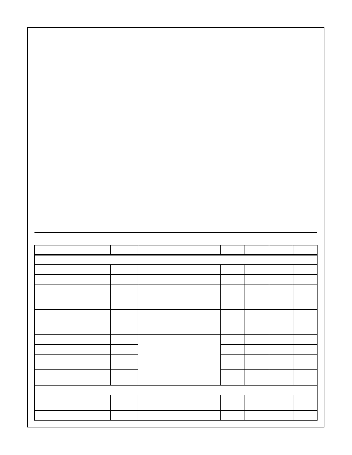
Electrical Specifications V
CC
PARAMETER SYMBOL TEST CONDITIONS MIN TYP MAX UNITS
OUTPUTS DRIVERS (DR0 TO DR7)
Output Channel Resistance r
Output Clamping Voltage V
Output Clamping Energy E
Peak Output Load Currents,
Short Duration
Cold Start-up Lamp Currents I
Output OFF Leakage Current I
Output Rise Time t
Output Fall Time t
Output Delay from Strobe, High to
Low Output Transition
Output Delay from Strobe, Low to
High Output Transition
LOGIC SUPPLY
Logic Supply Current, Loaded I
Logic Supply Current, No Load I
= 4.5V to 5.5V, V
DS(ON)
OC
OC
I
PEAK
Output Current = 200mA, TA=85oC 2 3.5 Ω
Outputs OFF 42 50 58 V
5ms Pulse, TA = 25oC 75 190 mJ
100µs Duration, Each Output, all
Outputs ON, Duty Cycle ≤ 2%
LAMP
5ms Duration, Each Output, all
Outputs ON, Duty Cycle ≤ 17%
OFF
rise
t
DHL
t
DLH
CC
fall
Output Voltage = 40V, TA=85oC - -0.2 10 µA
Load = 75Ω, 0.01µF (RC in Parallel),
V
BATT
All Outputs ON, 200mA Load at each
Output
CC
All Outputs OFF - - 100 µA
= 8V to 16V, TA = -40oC to 85oC, Unless Otherwise Specified.
BATT
0.85 - - A
0.3 - - A
0.5 4 30 µs
= 18V
0.5 10 30 µs
1410µs
0.2 2.6 10 µs
- - 100 µA
2
 Loading...