Intersil Corporation HIP0050 Datasheet

December 1996
HIP0050
0.3A/50V Octal Low Side Power Driver with
Serial Bus Control and Over-Current Fault Flag
Features
• Octal NDMOS Output Drivers in a High Voltage
Power BiMOS Process
- Each Capable of Sinking 300mA
- Low Idle and Standby Current
• Over-Stress Protection - Each Output:
- Over-Current Latch Off . . . . . . . . . 300mA Min
- Over-Voltage Clamp . . . . . . . . . . . . . . . 50V Typ
• Thermal Shutdown with Hysteresis
• Serial Data Input, Parallel Output Power Drive
• Short Circuit Latch Off for Each Output
• Common Enable for Output Drivers and
Data Storage Register
• Ambient Operating
Temperature Range. . . . . . . . . . . . .-40
- Optional 125
o
C Maximum Ambient Operating
o
C to 85oC
Temperature Range (Dissipation Limited)
Applications
• Automotive and Industrial Systems
• Solenoids, Relays and Lamp Drivers
• Logic and µP Controlled Drivers
• Robotic Controls
Description
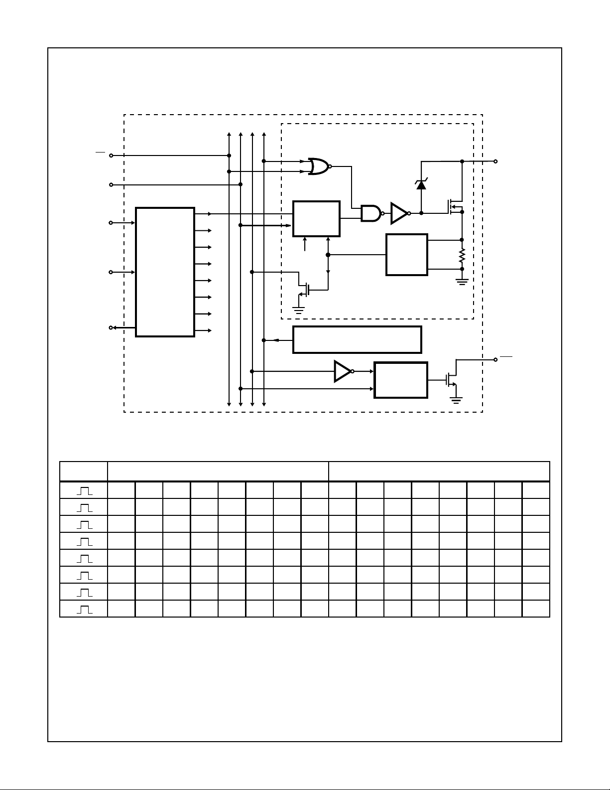
The HIP0050 is a logic controlled, eight channel Octal Low Side
Power Driver. As shown in the block diagram, the outputs are controlled via the serial data interface which allows the data to be
shifted out, allowing control of other cascaded serial devices. If an
Over-Current (OC) short circuit exists in one output, it may be independently shutdown while the other outputs remain in operation.
When a shorted output is latched off, it may be turned back on
when the next serial input data is latched. A fault flag (
FLT) is set to
a low status to indicate current-limited shutdown. The outputs are
independently latched off when an OC fault is detected. The fault
latch is cleared on the next data strobe. Over-Temperature (OT)
shutdown is provided with hysteresis to force global shutdown of
all output drivers. Shutdown is maintained until the on-chip temperature falls below the minimum hysteresis threshold point.
The HIP0050 is fabricated in a Power B iMOS IC process, and is
intended for use in automotive and other applications having a
wide range of temperature and electrical stress conditions. It is
particularly suited for driving lamps, displays, relays, and solenoids in
applications where low operating power, high breakdown voltage,
and high output current at high temperature is required. Higher
current needs can be met by paralleling adjacent output drivers
.
Ordering Information
PART
NUMBER
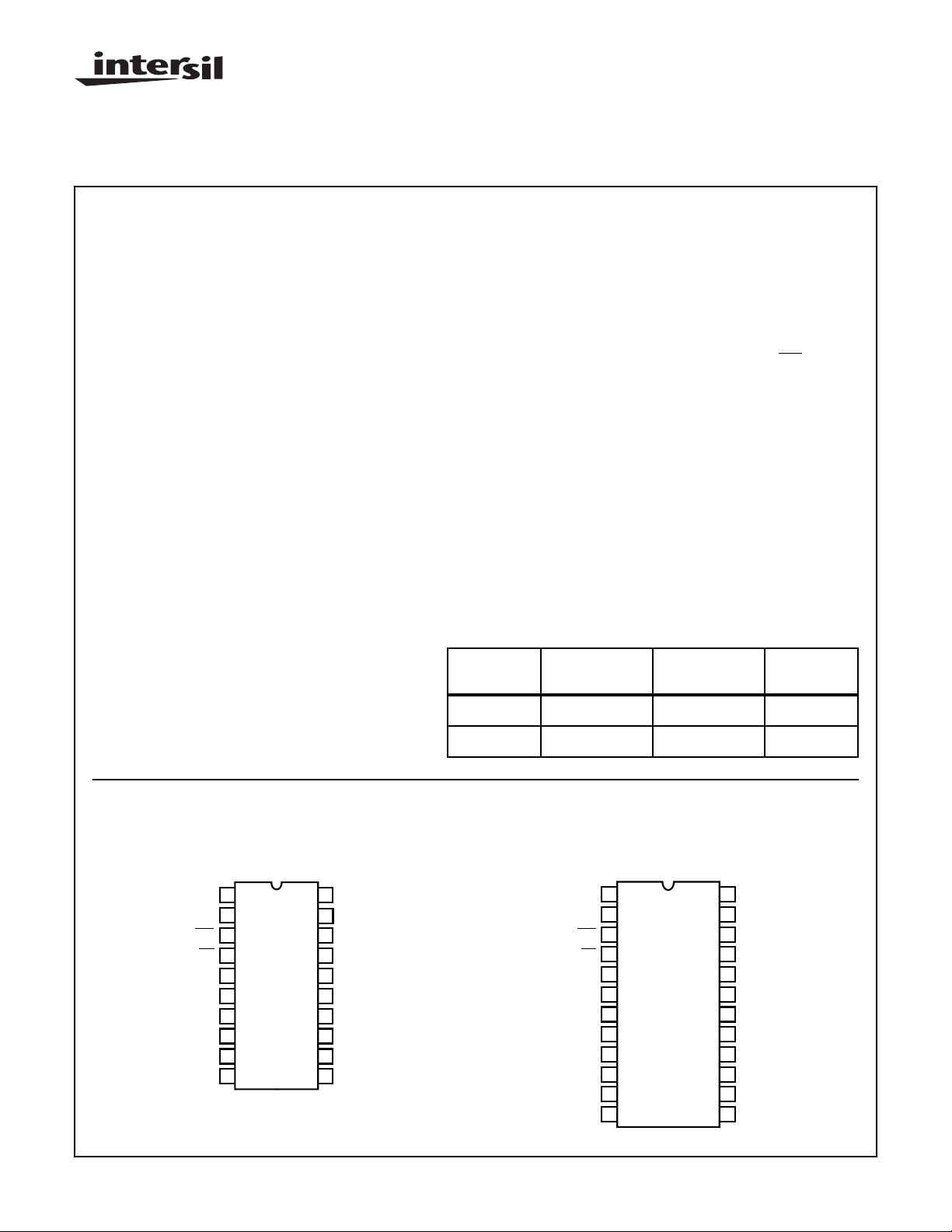
HIP050IP -40 to 85 20 Ld PDIP E20.3
TEMP.
RANGE (oC) PACKAGE PKG. NO.
HIP0050IB -40 to 85 24 Ld SOIC M24.3
Pinouts
HIP0050
(PDIP)
TOP VIEW
1
DR2
DR3
2
FLT
3
EN
4
GND
5
GND
6
STR
7
8
SCK
9
DR4
DR5
10
CAUTION: These devices are sensitive to electrostatic discharge; follow proper IC Handling Procedures.
http://www.intersil.com or 407-727-9207
| Copyright © Intersil Corporation 1999
20
19
18
17
16
15
14
13
12
11
DR1
DR0
SI
V
CC
GND
GND
LGND
SO
DR7
DR6
1
DR2
DR3
FLT
EN
GND
GND
GND
GND
STR
SCK
DR4
DR5
1
2
3
4
5
6
7
8
9
10
11
12
HIP0050
(SOIC)
TOP VIEW
24
DR1
23
DR0
22
SI
V
21
CC
20
GND
19
GND
18
GND
17
GND
16
LGND
15
SO
14
DR7
DR6
13
File Number
4034.1

Block Diagram
EN
STR
(ENABLE)
(STROBE)
HIP0050
OUTPUT DRIVER
(CHANNEL 1 OF 8)
DR#0
SCK
SO
Q0
SI
SERIAL
(SPI)
INPUT
REGISTER
(DATA IS
PARALLEL
OUTPUT
LATCHED
WHEN
STROBED)
Q1
Q2
Q3
Q4
Q5
Q6
Q7
OUTPUT
LATCH
POR
OVER-TEMPERATURE
SHUTDOWN W/HYS
S
R
OC
SHUT-
DOWN
FAULT
LATCH
Output Control Logic Table
STROBE 8-BIT SERIAL DATA (LATCHED) OUTPUT
D1 D2 D3 D4 D5 D6 D7 D8 DR1 DR2 DR3 DR4 DR5 DR6 DR7 DR8
00000000OFFOFFOFFOFFOFFOFFOFFOFF
10000000ONOFFOFFOFFOFFOFFOFFOFF
11000000ONONOFFOFFOFFOFFOFFOFF
11100000ONONONOFFOFFOFFOFFOFF
11110000ONONONONOFFOFFOFFOFF
00001111OFFOFFOFFOFFONONONON
11111111ONONONONONONONON
FLT
2

HIP0050
Absolute Maximum Ratings Thermal Information
Output Voltage, V
Input Voltage, VIN. . . . . . . . . . . . . . . . . . . . . . . . -0.3V to VCC +0.3V
Logic Supply Voltage, VCC . . . . . . . . . . . . . . . . . . . . . . -0.3V to +7V
Max Output Load Current, I
Max. Output Load Current, I
Operating Ambient Temperature Range, TA. . . . . . . . -40oC to 85oC
Operating Junction Temperature Range. . . . . . . . . . -40oC to 150oC
Storage Temperature Range, T
Maximum Lead Temperature (Soldering 10s Max). . . . . . . . . 300oC
(Lead Tips Only)
CAUTION: Stresses above those listed in “Absolute Maximum Ratings” may cause permanent damage to the device. This is a stress only rating and operation
of the device at these or any other conditions above those indicated in the operational sections of this specification is not implied.
Operating Conditions
Typical Logic Supply Voltage, VCC. . . . . . . . . . . . . . . . . . . . . .+5V
ICC Supply Current, with 200mA each Output . . . . . . . . . . . . 2mA
ICC Supply Current, with No Load . . . . . . . . . . . . . . . . . . . . . 2mA
Input Low Voltage. . . . . . . . . . . . . . . . . . . . . . . . . . . . . . . . . . 1.0V
Input High Voltage . . . . . . . . . . . . . . . . . . . . . . . . . . . . . . . . . 3.5V
(Note 1) . . . . . . . . . . . . . . . . . . . -0.3V to V
OUT
(Per Output, Note 2). . . . . . . . . I
LOAD
(All Outputs ON, Note 2). . . . . 2A
LOAD
. . . . . . . . . . . . . -55oC to 150oC
STG
OC
CL
Package
PDIP . . . . . . . . . . . . . 10 50 35
θJC(oC/W)† θJA (oC/W)††
02
SOIC . . . . . . . . . . . . . 10 60 40
† Versus Additional Square Inches 1oz. copper on PCB.
†† Standard Test Board, 0.002 diameter T/C located at lead
shoulder, middle lead.
Power Output Driver Voltage Range. . . . . . . . . . . . . . . . . 0 to V
Power Output Driver Current Load, IDR. . . . . . . . . . . . . . . . 0 to I
Typical Output r
Typical Output Rise Time . . . . . . . . . . . . . . . . . . . . . . . . . . . . . 4µs
Typical Output Fall Time . . . . . . . . . . . . . . . . . . . . . . . . . . . . .10µs
Channel Resistance . . . . . . . . . . . . . . . . 2Ω
DSON
OC
CL
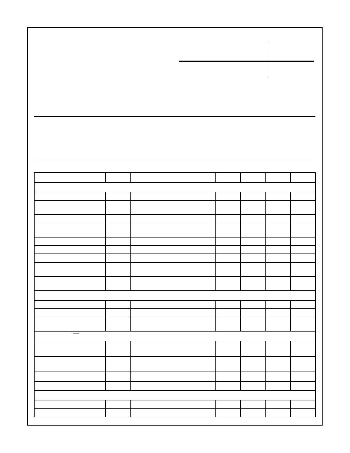
Electrical Specifications V
= 4.5V to 5.5V, V
CC
= 8V to 16V, TA = -40oC to 85oC; Unless Otherwise Specified
BATT
PARAMETER SYMBOL CONDITIONS MIN TYP MAX UNITS
OUTPUTS DRIVERS (DR0 TO DR7)
Output Channel Resistance r
Output Over-Current Shutdown
Threshold
Output Clamping Voltage V
Output Clamping Energy
Output OFF Leakage Current I
Output Rise Time t
Output Fall Time t
Output Delay from Strobe, High
to Low Output Transition
Output Delay from Strobe, Low to
High Output Transition
DSON
I
E
OFF
RISE
FALL
t
DHL
t
DLH
Output Current = 200mA, TA=85oC - 2 4.0 Ω
CL
Outputs OFF 42 50 58 V
OC
1ms Single Pulse Width, TA= 25oC,
OC
(Refer to Figure 2 for SOA).
Output Voltage = 40V, TA=85oC--10µA
Load = 75Ω, 0.01µF (Parallel) 0.5 4 30 µs
Load = 75Ω, 0.01µF (Parallel) 0.5 10 30 µs
LOGIC SUPPLY
Logic Supply Current, Loaded I
Logic Supply Current, No Load I
Logic Supply Under-Voltage
Reset Threshold
All Outputs ON, 0.2A Load Per Output - 2 4 mA
CC
All Outputs OFF - 2 4 mA
CC
All Outputs OFF 3.5 - 4 V
LOGIC INPUTS (EN, SI, SCK, STR)
Threshold Voltage at Falling
VT-VCC = 5V ±10% 0.2V
Edge
Threshold Voltage at Rising
VT+VCC = 5V ±10% - 0.6V
Edge
Hysteresis Voltage V
Leakage Current
I
VT+ - VT- 0.85 1.4 2.25 V
H
LIN
SERIAL DATA CLOCK (SCK) (Refer to Figure 1 for Waveform Detail)
Frequency f
Pulse Width High t
SCK
W(SCKH)
300 - 500 mA
-25-mJ
1410µs
0.2 2.6 10 µs
CC
0.3V
CC
CC
-V
0.7V
CC
V
-10 - 10 µA
- - 1.6 MHz
- 27 175 ns
3
 Loading...