HIP0045
Data Sheet April 1999
1A/50V Octal Low Side Power Driver With
Serial Bus Control and Fault Protection
The HIP0045 is a logic controlled, eight channel Octal Serial
Pow er Low Side Driv er. The serial peripheral interface (SPI)
utilized by the HIP0045 is a serial synchronous bus compatible
with Intersil CDP68HC05, or equivalent, microcomputers. As
shown in the Block Diagram f or the HIP0045, each of the open
drain MOS Output Drivers have individual protection f or o v ervoltage and over-current. Each output channel has separate
output latch control with fault unlatch and diagnostic or status
feedback.Undernormal ON conditions, each output driveris in
a low voltage, high current state of saturated turn-on.
Comparators in the diagnostic circuitry monitor the output
drivers to determine if an out of saturation condition exists. If a
fault is sensed, the respective output driver f or Channels 0 - 5
haveovercurrentlatch-off .Channels6 and 7 are configured for
lamp drivers and have current limiting with ov er-temper ature
latch-off. Channels 0 and 1 have direct par allel drive control for
PWM applications and are ORed with the SPI Bus control. All
channels are SPI Bus controlled and sense the output states
for diagnostic feedbac k.
The HIP0045 is fabricated in a Power BiMOS IC process,
and is intended for use in automotive and other applications
having a wide range of temperature and electrical stress
conditions. It is particularly suited for driving relays,
solenoids and lamps in applications where low standby
power, high operating voltage, and high output current in
high ambient temperature conditions is required.
The HIP0045 is in a 20 lead plastic Pow er SOP (PSOP)
Packagewithanintegralcopper‘slug’toconductheatdirectly
to a PCB interface or heat sink on the bottom of the package.
Ordering Information
PART NO. TEMP. RANGE (oC) PACKAGE PKG. NO.
HIP0045AB -40 to 125 20 Ld PSOP M20.433
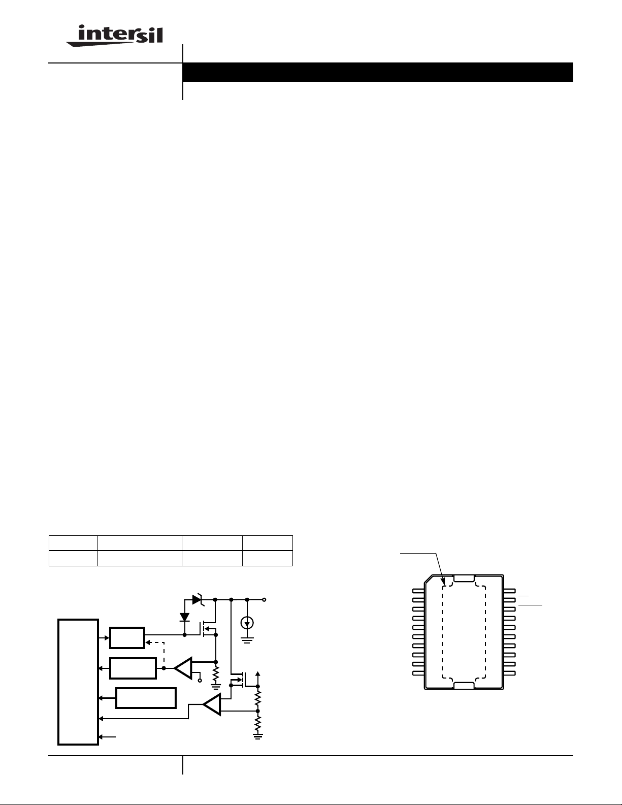
Driver Block Diagram
OUT
I
SK
V
CC
V
REF
SPI AND
DIRECT
INPUT
CONTROL
WITH
FAULT/
STATUS
OUTPUT
DRIVER
OC LATCH
(CH. 0-5)
OVER-TEMP.
DET. (CH. 6, 7)
RESET
OC LIMIT
(CH. 6, 7)
-
+
FAULT/STATUS
OC
REF
+
-
File Number
4047.2
Features
• Octal NDMOS Output Drivers in a High Voltage Power
BiMOS Process
• Over-Stress Protection - Each Output:
- Over-Current Protection . . . . . . . . . . . . . . . . . . . 1A Min
- Over-Voltage Clamp Protection . . . . . . . . . . . . 50V Typ
- Thermal Shutdown Protection (2 Channels)
• Open-Load Detection
• Power BiMOS Output Configuration
- Current Latch-Off Protection for 6 Channels; 2 with
External Drive Input and ORed with SPI Bus Control
- 2 Channels Configured for Lamp Drivers with Current
Limiting and Over-Temperature Latch-Off
• High Speed CMOS Logic Control
- SPI Bus Controlled Interface
- Individual Output Latch
- Individual Fault Unlatch and Feedback
- Common Reset Line
• Low Quiescent Current . . . . . . . . . . . . . . . . . . . 5mA Max
• Ambient Operating Temp. Range. . . . . . . -40
o
C to 125oC
Applications
• Automotive and Industrial Systems
• Solenoids, Relays and Lamp Drivers
• Logic and µP Controlled Drivers
• Robotic Controls
Pinout
HIP0045 (PSOP WITH HEAT SLUG)
TOP VIEW
INTEGRAL COPPER
HEAT SINK ‘SLUG’
FOR PCB CONTACT
OR EXT. HEAT SINK
GND
IN0
MISO
OUT0
OUT2
OUT4
OUT6
MOSI
SCK
GND
1
2
3
4
5
6
7
8
9
10
GND
20
CE
19
RESET
18
OUT7
17
OUT5
16
OUT3
15
OUT1
14
V
13
12
11
CC
IN1
GND
4-1
CAUTION: These devices are sensitive to electrostatic discharge; follow proper IC Handling Procedures.
http://www.intersil.com or 407-727-9207
| Copyright © Intersil Corporation 1999

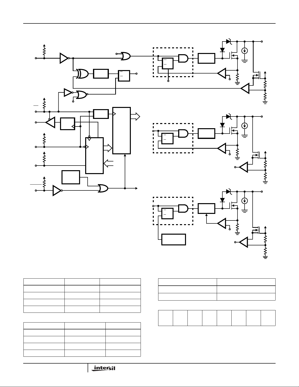
Detailed Block Diagram
HIP0045
SPI
REG
ON/OFF
FILTER
FILTER
OUT
Q0, 1
LATCH
FAULT LATCH
DIAG0-7
S
R
8-BIT
OUTPUT
LATCH
IN 0, 1
CE
MISO
SCK
MOSI
RESET
V
CC
V
CC
V
CC
V
CC
V
CC
RESET
Q
LOW
VOTAGE
RESET
D
SHIFT
IN
NOTES:
1. OC = Over-Current Voltage Ref. = 1.8V Typ.
2. ISK = Current Sink Pull-Down = 500µA Typ.
3. Diag0, 1 = Status bit when Q0, 1 controlling OUT0, 1.
4. Diag0, 1 = Fault bit when IN1, 0 controlling OUT0, 1.
5. Refer to text and Tables 6, 7 for diagnostic information.
Q
DIAG0, 1
STATUS/
FAULT
Q0-7
ON/OFF
LATCH
RESET
ON/OFF
LATCH
Q2 - 5
Q6, 7
OVERLOAD LATCH
QS
R
RESET
OVERLOAD LATCH
QS
R
OVERLOAD LATCH
QS
R
OVER-TEMP.
DET.
DRIVER
DRIVER
DRIVER
-
+
OC
REF
-
+
OC
REF
DIAG2-5
STATUS
-
+
OC
REF
DIAG6, 7
STATUS
I
OUT0, 1
SK
V
CC
V
+
REF
-
I
OUT2-5
SK
V
CC
+
V
REF
-
I
OUT6, 7
SK
V
CC
+
V
REF
-
Input to Output Control Tables
TABLE 1. OUTPUT 0
SPI BIT 0 IN0 OUT0
0 1 OFF
00ON
10ON
11ON
TABLE 2. OUTPUT 1
SPI BIT 1 IN1 OUT1
0 1 OFF
00ON
10ON
11ON
4-2
TABLE 3. OUTPUT 2 - 7
SPI BIT 2 - 7 OUT2 - 7
0 OFF
1ON
TABLE 4. OUTPUT CONTROL REGISTER, Q0 - 7
Q1 Q3 Q5 Q7 Q0 Q2 Q4 Q6
(D7I) (D6I) (D5I) (D4I) (D3I) (D2I) (D1I) (D0I)
MSB LSB
NOTE: The OutputControl Register bitsQ0 -7 have thesame order
asthe Diagnostic FailureRegister bits Diag0- 7as definedin Table 5.
Data bits D0I - D7I give the MOSI SPI serial data input flow
sequence.

HIP0045
Absolute Maximum Ratings Thermal Information
Maximum Output Voltage, V
Peak Output Load Current, I
Continuous Output Load Current, I
Continuous Output Load Current, I
Total Average Current, I
OUT
Reverse Peak Current Drive, Any one Output, IRD; t ≤ 2ms . . . -3A
DC Logic Supply, VCC. . . . . . . . . . . . . . . . . . . . . . . . . . . . -0.3 to 7V
Input Voltage, All Inputs and Data Lines . . . . . . . -0.3 to VCC+0.3V
Operating Conditions
Temperature Range. . . . . . . . . . . . . . . . . . . . . . . . . -40oC to 125oC
Logic Supply Voltage, VCC . . . . . . . . . . . . . . . . . . . . . 4.5V to 5.5V
CAUTION: Stresses above those listed in “Absolute Maximum Ratings” may cause permanent damage to the device. This is a stress only rating and operationofthe
device at these or any other conditions above those indicated in the operational sections of this specification is not implied.
NOTE:
6. θJA Rated with standard PC Board, θJC rated with infinite heat sink.
. . . . . . . . . . . . . . . . . . .-0.7 to V
OUT
. . . . . As Specified for ISC, I
LOAD
(All 8 Outputs ON) . . . . 0.5A
OUT
(Any one Output ON) . . 1A
OUT
OC
LIM
(All 8 Outputs) . . . . . . . . . . . . . . . 4.5A
Thermal Resistance (Typical, Note 6) θJA (oC/W) θJC (oC/W)
PSOP Package . . . . . . . . . . . . . . . . . . 40 2
Maximum Junction Temperature, TJ . . . . . . . . . . . . . . . . . . . .150oC
Maximum Storage Temperature Range, T
. . . . -55oC to 150oC
STG
Maximum Lead Temperature (Soldering 10s) . . . . . . . . . . . . .265oC
Die Characteristics
Back Side Potential . . . . . . . . . . . . . . . . . . .V- (GND Pin, Heat Sink)
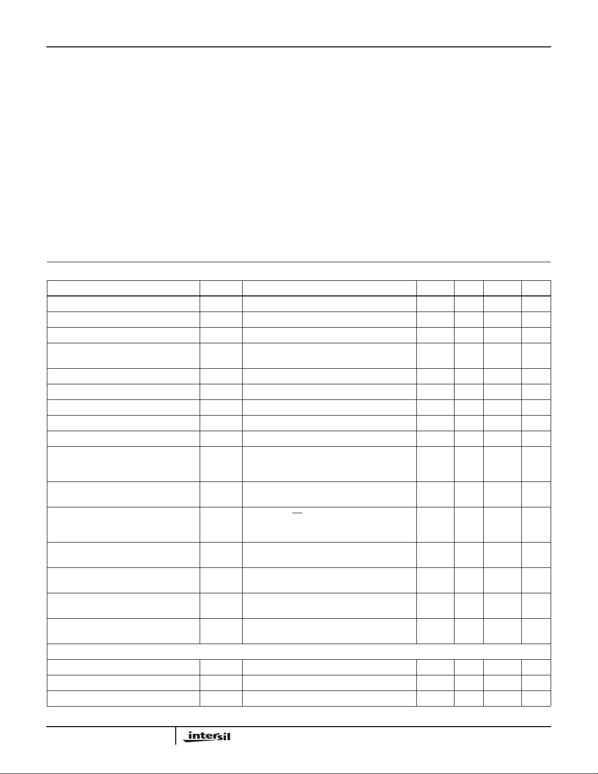
Electrical Specifications V
= 4.5V to 5.5V, TA = -40oC to 125oC, Unless Otherwise Specified
CC
PARAMETER SYMBOL TEST CONDITIONS MIN TYP MAX UNITS
Standby Current, No Load I
Supply Current, Full Load I
Output Clamping Voltage (Note 7) V
Output Clamping Energy E
CCO
No Load - - 5 mA
All Outputs ON, 0.5A Load Per Output - - 5 mA
CC
OCILOAD
1ms Single Pulse Width, TA = 25oC,
OC
(Refer to Figure 4 for SOA)
Output Leakage Current 1 (Note 8) I
Output Leakage Current 2 (Note 8) I
Output Leakage Current 3 (Note 8) I
Drain-to-Source On Resistance, OUT0 - 7 r
Output Capacitance C
Turn-On Delay, OUT0, 1 t
Turn-On Delay, OUT2 - 7 t
Turn-Off Delay t
Turn-On Voltage Slew-Rate, OUT2 - 7 For V
Turn-On Voltage Slew-Rate, OUT0, 1 ForV
Turn-Off Voltage Slew-Rate, OUT0 - 7 For V
Turn-Off Voltage Slew-Rate, OUT0 - 7 For V
O LEAK1VOUT
O LEAK2VOUT
O LEAK3VOUT
DSONILOAD
OUTVOUT
d(ON)RL
d(ON)RL
d(OFF)RL
dV
-------------------
dV
-------------------
dV
----------------------
dV
----------------------
ON1
dt
ON2
dt
OFF1
dt
OFF2
dt
V
IN0,1
V
BATT
V
BATT
V
IN0,1
V
BATT
RL = 500Ω
RL = 500Ω
RL = 500Ω
V
BATT
FAULT PARAMETERS
Reverse Current Drive, OUT0 - 7 I
Reverse Voltage Drop, OUT0 - 7 V
∆ICC during Reverse Current Drive ∆I
RD
RDIOUT
CCIOUT
= 0.5A, Output Programmed OFF 45 - 62 V
20 45 - mJ
= 25V, Outputs OFF - - 100 µA
= 16V, Outputs OFF - - 100 µA
= 16V, Outputs OFF, VCC = 1V - - 10 µA
= 0.5A; TJ = 150oC - - 1.5 Ω
= 16V, f = 1MHz - - 20 pF
= 500Ω, VCE = 50% to V
= 50% to V
OUT
= 0.9 x V
OUT
= 0.9 x V
,
BATT
BATT
,
--5µs
= 16V
= 500Ω, VCE = 50% to V
OUT
= 0.9 x V
BATT
,
--10µs
= 16V
= 500Ω, VCE = 50% to V
= 50% to V
OUT
= 0.9 x V
OUT
= 0.1 x V
,
BATT
BATT
,
--10µs
= 16V
= 90%to 30% ofV
OUT
= 90% to30% of V
OUT
= 30% to90% of V
OUT
= 30% to 80% of V
OUT
BATT;VBATT
BATT;VBATT
BATT;VBATT
OC;
= 16V,
= 16V,
= 16V,
- 0.7 3.5 V/µs
- 2 10 V/µs
- 2 10 V/µs
- 2 15 V/µs
= 0.9 x VOC, RL = 500Ω
-500 - - mA
= -3A, t ≤2ms -1.5 - - V
= -3A, t ≤2ms - - 100 mA
4-3
 Loading...