Intersil Corporation HIN241IA, HIN241, HIN238, HIN237IP, HIN237IB Datasheet
...
TM
HIN230 thru HIN241
Data Sheet May 2000
+5V Powered RS-232
Transmitters/Receivers
The HIN230-HIN241 family of RS-232 transmitters/receivers
interfacecircuits meet all ElA RS-232E and V.28specifications,
and are particularly suited forthose applications where ±12V is
not available . The y require a single +5V po wer supply (except
HIN231 and HIN239) and feature onboard charge pump
voltage converters which generate +10V and -10V supplies
from the 5V supply. The HIN233 and HIN235 require no
externalcapacitors and are ideally suited for applications where
circuit board space is critical. The family of devices offer a wide
variety of RS-232 transmitter/receiver combinations to
accommodate various applications (see Selection Table).
The drivers feature true TTL/CMOS input compatibility, slewrate-limited output, and 300Ω power-off source impedance.
The receivers can handle up to ±30V, and have a 3kΩ to 7kΩ
input impedance. The receivers also feature hysteresis to
greatly improve noise rejection.
File Number 3138.7
Features
• Meets All RS-232E and V.28 Specifications
• Requires Only Single +5V Power Supply
- (+5V and +12V - HIN231 and HIN239)
• High Data Rate. . . . . . . . . . . . . . . . . . . . . . . . . . .120kbps
• HIN233 and HIN235 Require No External Capacitors
• Onboard Voltage Doubler/Inverter
• Low Power Consumption
• Low Power Shutdown Function
• Three-State TTL/CMOS Receiver Outputs
• Multiple Drivers
- ±10V Output Swing for 5V lnput
- 300Ω Power-Off Source Impedance
- Output Current Limiting
- TTL/CMOS Compatible
- 30V/µs Maximum Slew Rate
• Multiple Receivers
- ±30V Input Voltage Range
-3kΩ to 7kΩ Input Impedance
- 0.5V Hysteresis to Improve Noise Rejection
Applications
• Any System Requiring RS-232 Communication Ports
- Computer - Portable, Mainframe, Laptop
- Peripheral - Printers and Terminals
- Instrumentation
- Modems
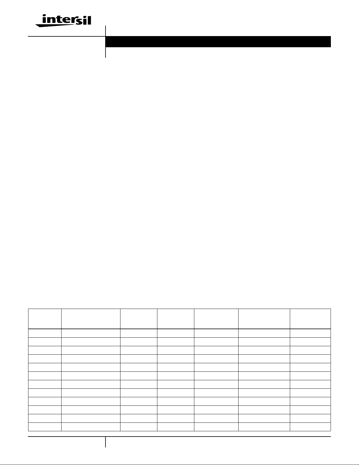
Selection Table
NUMBER OF
PART
NUMBER
HIN230 +5V 5 0 4 Capacitors Yes/No 20
HIN231 +5V and +7.5V to 13.2V 2 2 2 Capacitors No/No 16
HIN232 +5V 2 2 4 Capacitors No/No 16
HIN233 +5V 2 2 None No/No 20
HIN234 +5V 4 0 4 Capacitors No/No 16
HIN235 +5V 5 5 None Yes/Yes 24
HIN236 +5V 4 3 4 Capacitors Yes/Yes 24
HIN237 +5V 5 3 4 Capacitors No/No 24
HIN238 +5V 4 4 4 Capacitors No/No 24
HIN239 +5V and +7.5V to 13.2V 3 5 2 Capacitors No/Yes 24
HIN240 +5V 5 5 4 Capacitors Yes/Yes 44
HIN241 +5V 4 5 4 Capacitors Yes/Yes 28
POWER SUPPLY
VOLTAGE
RS-232
DRIVERS
NUMBER OF
RS-232
RECEIVERS
EXTERNAL
COMPONENTS
LOW POWER
SHUTDOWN/TTL
THREE-ST ATE
NUMBER OF
LEADS
3-1
1-888-INTERSIL or 321-724-7143 | Intersil and Design is a trademark of Intersil Corporation. | Copyright © Intersil Corporation 2000
CAUTION: These devices are sensitive to electrostatic discharge; follow proper IC Handling Procedures.

Ordering Information
HIN230 thru HIN241
PART
NUMBER
HIN230CB 0 to 70 20 Ld SOIC M20.3
HIN230IB -40 to 85 20 Ld SOIC M20.3
HIN231CB 0 to 70 16 Ld SOIC M16.3
HIN231CP 0 to 70 14 Ld PDIP E14.3
HIN231IB -40 to 85 16 Ld SOIC M16.3
HIN231IP -40 to 85 14 Ld PDIP E14.3
HIN232CP 0 to 70 16 Ld PDIP E16.3
HIN232CB 0 to 70 16 Ld SOIC M16.3
HIN232IP -40 to 85 16 Ld PDIP E16.3
HIN232IB -40 to 85 16 Ld SOIC M16.3
HIN233CP 0 to 70 20 Ld PDIP E20.3
HIN234CB 0 to 70 16 Ld SOIC M16.3
HIN234IB -40 to 85 16 Ld SOIC M16.3
HIN235CP 0 to 70 24 Ld PDIP E24.6
HIN236CP 0 to 70 24 Ld PDIP E24.3
HIN236CB 0 to 70 24 Ld SOIC M24.3
HIN236IP -40 to 85 24 Ld PDIP E24.3
HIN236IB -40 to 85 24 Ld SOIC M24.3
TEMP.
RANGE (oC) PACKAGE PKG. NO.
PART
NUMBER
HIN237CP 0 to 70 24 Ld PDIP E24.3
HIN237CB 0 to 70 24 Ld SOIC M24.3
HIN237IP -40 to 85 24 Ld PDIP E24.3
HIN237IB -40 to 85 24 Ld SOIC M24.3
HIN238CP 0 to 70 24 Ld PDIP E24.3
HIN238CB 0 to 70 24 Ld SOIC M24.3
HIN238IP -40 to 85 24 Ld PDIP E24.3
HIN238IB -40 to 85 24 Ld SOIC M24.3
HIN239CB 0 to 70 24 Ld SOIC M24.3
HIN239CP 0 to 70 24 Ld PDIP E24.3
HIN239IB -40 to 85 24 Ld SOIC M24.3
HIN240CN 0 to 70 44 Ld MQFP Q44.10X10
HIN240IN -40 to 85 44 Ld MQFP Q44.10X10
HIN241CB 0 to 70 28 Ld SOIC M28.3
HIN241IB -40 to 85 28 Ld SOIC M28.3
HIN241CA 0 to 70 28 Ld SSOP M28.209
HIN241IA -40 to 85 28 Ld SSOP M28.209
NOTE: Manyof the surface mountdevicesare availableon tape and
reel; add -T to suffix.
TEMP.
RANGE (oC) PACKAGE PKG. NO.
Pin Descriptions
PIN FUNCTION
V
CC
V+ Internally generated positive supply (+10V nominal), HIN231 and HIN239 require +7.5V to +13.2V.
V- Internally generated negative supply (-10V nominal).
GND Ground lead. Connect to 0V.
C1+ External capacitor (+ terminal) is connected to this lead.
C1- External capacitor (- terminal) is connected to this lead.
C2+ External capacitor (+ terminal) is connected to this lead.
C2- External capacitor (- terminal) is connected to this lead.
T
IN
T
OUT
R
IN
R
OUT
EN Enable input. This is an active low input which enables the receiver outputs. With EN = 5V,the outputs are placed in a high
SHUTDOWN Shutdown Input. With SHUTDOWN = 5V, the charge pump is disabled, the receiver outputs are in a high impedance state
NC No Connect. No connections are made to these leads.
Power Supply Input 5V±10%.
Transmitter Inputs. These leads accept TTL/CMOS levels. An internal 400kΩ pull-up resistor to VCCis connected to each lead.
Transmitter Outputs. These are RS-232 levels (nominally ±10V).
ReceiverInputs. These inputs acceptRS-232 input levels.An internal 5kΩpull-down resistor to GNDis connected to each input.
Receiver Outputs. These are TTL/CMOS levels.
impedance state.
and the transmitters are shut off.
3-2

Pinouts
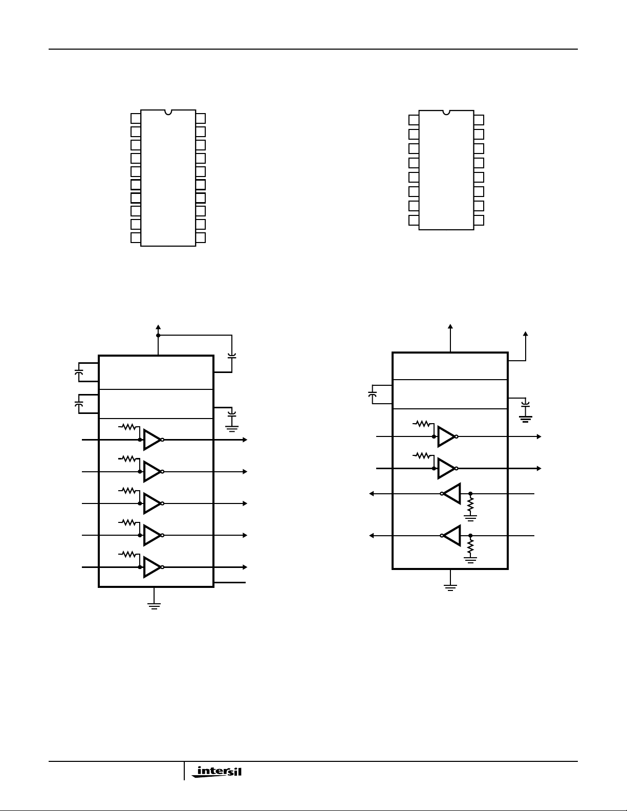
HIN230 (SOIC)
TOP VIEW
HIN230 thru HIN241
HIN231 (SOIC)
TOP VIEW
1
T3
OUT
2
T1
OUT
3
T2
OUT
4
T2
IN
5
T1
IN
6
GND
7
V
CC
8
C1+
9
V+
10
C1-
+5V
8
C1+
+
1µF
10
C1-
11
C2+
+
1µF
12
C2-
+5V
400kΩ
T1
T2
T3
T4
T5
5
IN
+5V
400kΩ
4
IN
+5V
400kΩ
14 1
IN
+5V
400kΩ
15 20
IN
+5V
IN
400kΩ
V
CC
+5V TO 10V
VOLTAGE DOUBLER
+10V TO -10V
VOLTAGE INVERTER
T1
T2
T3
T4
T5
20
T4
OUT
19
T5
IN
18
NC
17
SHUTDOWN
16
T5
OUT
15
T4
IN
14
T3
IN
13
V-
12
C2-
11
C2+
R2
T2
OUT
R2
OUT
T2
C+
NC
1
2
C-
3
V-
4
5
IN
6
7
IN
8
16
V+
(14)
V
CC
GND
T1
R1
R1
T1
NC
OUT
IN
OUT
IN
(13)
(12)
(11)
(10)
(9)
(8)
15
14
13
12
11
10
9
NOTE: Pin numbers in parentheses are for PDIP Package.
+5V
7
V+
V-
1µF
+
9
1
C+
+
13
1µF
1µF
+
2
3
T1
T2
T3
T4
OUT
OUT
OUT
OUT
R1
R2
T1
T2
OUT
OUT
2
10
IN
7
IN
VOLTAGE INVERTER
C-
+5V
400kΩ
+5V
400kΩ
15
V
CC
+12V TO -12V
T1
T2
R1
R2
1619
17
T5
OUT
SHUTDOWN
14
6
+7.5V TO +13.2V
V+
V-
5kΩ
5kΩ
16
3
1µF
+
13
4
1211
56
T1
T2
R1
R2
OUT
OUT
IN
IN
NOTE: SOIC pin numbers shown.
3-3

Pinouts (Continued)
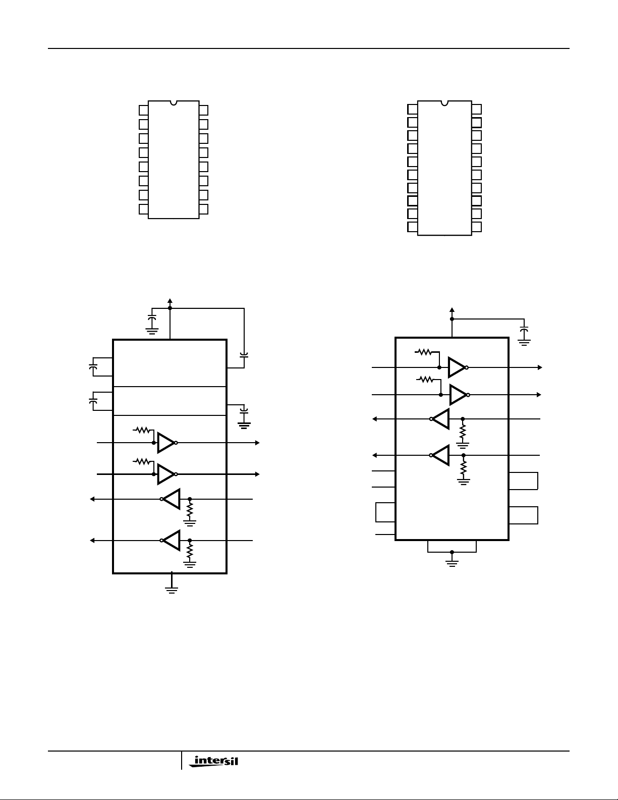
HIN232 (PDIP, SOIC)
TOP VIEW
HIN230 thru HIN241
HIN233 (PDIP, SOIC)
TOP VIEW
R1
R2
1µF
1µF
T1
T2
OUT
OUT
T2
C1+
C2+
OUT
R2
V+
C1-
C2-
V-
1
1
2
3
4
5
6
7
8
IN
16
V
CC
15
GND
14
T1
OUT
13
R1
IN
12
R1
OUT
11
T1
IN
10
T2
IN
9
R2
OUT
T2
T1
R1
OUT
R1
T1
OUT
GND
V
CC
(V+) C1+
GND
(V-) C2-
IN
2
IN
3
4
IN
5
6
7
8
9
10
20
19
18
17
16
15
14
13
12
11
R2
OUT
R2
IN
T2
OUT
VC2C2+
V+ (C1-)
C1- (C1+)
V- (C2+)
C2+ (C2-)
NOTE: Pin names in parentheses are for SOIC Package.
+5V
+
1µF
1
C1+
+
3
4
+
5
11
IN
10
IN
VOLTAGE DOUBLER
C1C2+
VOLTAGE INVERTER
C2-
+5V
400kΩ
+5V
400kΩ
16
V
CC
+5V TO 10V
+10V TO -10V
T1
T2
R1
R2
5kΩ
5kΩ
V+
1µF
+
2
T1
IN
+5V
2
400kΩ
+5V
IN
20
8 (13)
13 (14)
12 (10)
17
14 (8)
1
3
C1+
C1VVV+
6
V-
1µF
+
14
7
1312
89
T1
T2
R1
R2
OUT
OUT
IN
IN
T2
R1
OUT
R2
OUT
NO
CONNECT
INTERNAL
-10V
SUPPLY
INTERNAL
+10V
SUPPLY
400kΩ
GND
6
R1
R2
+5V
V
CC
+
6
T1
T2
0.1µF
5
18
4
T1
T2
R1
OUT
OUT
IN
5kΩ
5kΩ
C2+
C2+
C2-
C2-
19
11 (12)
15
16
10 (11)
R2
IN
GND
9
3-4
15
NOTE: Pin numbers in parentheses are for SOIC Package.

Pinouts (Continued)
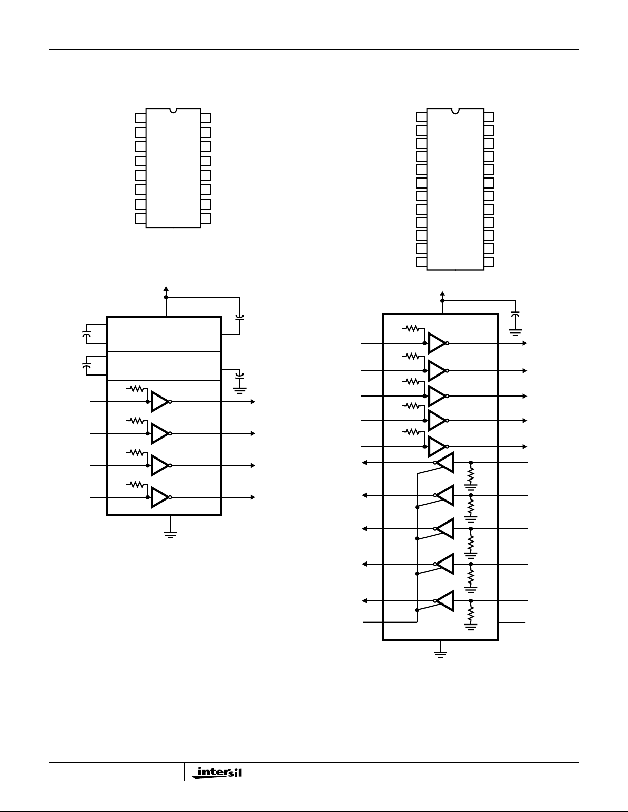
HIN234 (SOIC)
TOP VIEW
HIN230 thru HIN241
HIN235 (PDIP)
TOP VIEW
1
T1
OUT
2
T2
OUT
3
T2
IN
4
T1
IN
5
GND
6
V
CC
7
C1+
8
V+
+5V
7
C1+
+
1µF
1µF
T1
T2
T3
T4
9
C1-
10
C2+
+
11
4
IN
3
IN
13 16
IN
14 15
IN
VOLTAGE INVERTER
C2+5V
400kΩ
+5V
400kΩ
+5V
400kΩ
+5V
400kΩ
V
CC
+5V TO 10V
VOLTAGE DOUBLER
+10V TO -10V
T1
T2
T3
T4
T4
T3
T1
T2
R2
R1
OUT
OUT
OUT
OUT
R2
OUT
T2
T1
OUT
R1
GND
V
CC
1
2
3
4
5
IN
6
7
IN
8
IN
9
10
IN
11
12
16
T3
OUT
15
T4
OUT
14
T4
IN
13
T3
IN
12
V-
11
C2-
10
C2+
9
C1-
24
R3
23
R3
22
T5
IN
21
SHUTDOWN
20
EN
19
T5
OUT
18
R4
17
R4
16
T4
IN
15
T3
IN
14
R5
13
R5
IN
OUT
IN
OUT
OUT
IN
+5V
6
V+
V-
5
1µF
+
8
T1
IN
12
1µF
+
1
2
T1
T2
T3
T4
OUT
OUT
OUT
OUT
R1
R2
R3
R4
R5
T2
T3
T4
T5
OUT
OUT
OUT
OUT
OUT
IN
IN
IN
IN
EN
+5V
400kΩ
8
+5V
7
400kΩ
+5V
15
400kΩ
+5V
16
400kΩ
+5V
400kΩ
22
9
6
23
17
14
20
V
T1
T2
T3
T4
T5
R1
R2
R3
R4
R5
GND
CC
12
5kΩ
5kΩ
5kΩ
0.1µF
+
3
4
2
1
19
10
5
24
18
T1
T2
T3
T4
T5
R1
R2
R3
R4
OUT
OUT
OUT
OUT
OUT
IN
IN
IN
IN
5kΩ
5kΩ
13
21
R5
IN
SHUTDOWN
11
3-5
 Loading...