

Page 1
查询FN3138供应商
®
HIN232, HIN236, HIN237,HIN238,
HIN239, HIN240, HIN241
Data Sheet September 2004
+5V Powered RS-232
Transmitters/Receivers
The HIN232-HIN241 family of RS-232 transmitters/receivers
interface circuits meet all ElA RS-232E and V.28 specifications,
and are particularly suited for those applications where ±12V is
not available. They require a single +5V power supply (except
HIN239) and feature onboard charge pump voltage converters
which generate +10V and
The family of devices off er a wide variety of RS-232
transmitter/receiver combinations to accommodate various
applications (see Selection Table).
The drivers feature true TTL/CMOS input compatibility, slewrate-limited output, and 300Ω power-off source impedance.
The receivers can handle up to ±30V, and have a 3kΩ to 7kΩ
input impedance. The receivers also feature hysteresis to
greatly improve noise rejection.
-10V supplies from the 5V supply.
FN3138.14
Features
• Meets All RS-232E and V.28 Specifications
• Requires Only Single +5V Power Supply
- (+5V and +12V - HIN239)
• High Data Rate. . . . . . . . . . . . . . . . . . . . . . . . . . . 120kbps
• Onboard Voltage Doubler/Inverter
• Low Power Consumption
• Low Power Shutdown Function
• Three-State TTL/CMOS Receiver Outputs
• Multiple Drivers
- ±10V Output Swing for 5V lnput
-300Ω Power-O ff Sourc e Impedance
- Output Current Limiting
- TTL/CMOS Compatible
-30V/µs Maximum Slew Rate
• Multiple Receivers
- ±30V Input Voltage Range
-3kΩ to 7kΩ Input Impedance
- 0.5V Hysteresis to Improve Noise Rejection
• Pb-free available
Applications
• Any System Requiring RS-232 Communication Ports
- Computer - Portable, Mainframe, Laptop
- Peripheral - Printers and Terminals
- Instrumentation
- Modems
Selection Table
NUMBER OF
PART
NUMBER
HIN232 +5V 2 2 4 Capacitors No/No 16
HIN236 +5V 4 3 4 Capacitors Yes/Yes 24
HIN237 +5V 5 3 4 Capacitors No/No 24
HIN238 +5V 4 4 4 Capacitors No/No 24
HIN239 +5V and +7.5V to 13.2V 3 5 2 Capacitors No/Yes 24
HIN240 +5V 5 5 4 Capacitors Yes/Yes 44
HIN241 +5V 4 5 4 Capacitors Yes/Yes 28
POWER SUPPLY
VOLTAGE
RS-232
DRIVERS
NUMBER OF
RS-232
RECEIVERS
EXTERNAL
COMPONENTS
LOW POWER
SHUTDOWN/TTL
THREE-STATE
NUMBER OF
LEADS
1
CAUTION: These devices are sensitive to electrostatic discharge; follow proper IC Handling Procedures.
1-888-INTERSIL or 321-724-7143
| Intersil (and design) is a registered trademark of Intersil Americas Inc.
All other trademarks mentioned are the property of their respective owners.
Copyright © Intersil Americas Inc. 2004. All Rights Reserved.
Page 2
Pin Descriptions
PIN FUNCTION
HIN232, HIN236, HIN237, HIN238, HIN239, HIN240, HIN241
V
CC
V+ Internally generated positive supply (+10V nominal), HIN239 requires +7.5V to +13.2V.
V- Internally generated negative supply (-10V nominal).
GND Ground lead. Connect to 0V.
C1+ External capacitor (+ terminal) is connected to this lead.
C1- External capacitor (- terminal) is connected to this lead.
C2+ External capacitor (+ terminal) is connected to this lead.
C2- External capacitor (- terminal) is connected to this lead.
T
IN
T
OUT
R
IN
R
OUT
EN
SD Shutdown Input. With SD = 5V, the charge pump is disabled, the receiver outputs are in a high impedance state and the
NC No Connect. No connections are made to these leads.
Power Supply Input 5V ±10%.
Transmitter Inputs. These leads accept TTL/CMOS levels. A n internal 400kΩ pull-up resistor to V
Transmitter Outputs. These are RS-232 levels (nominally ±10V).
Receiver Inputs. These inputs accept RS-232 input le vels . An internal 5kΩ pull-dow n resistor to GND is connected to each input.
Receiver Outputs. These are TTL/CMOS levels.
Enable input. This is an active low input which enables the receiver outputs. With EN = 5V, the receiver outputs are placed in
a high impedance state.
transmitters are shut off.
is connected to each lead.
CC
2
Page 3
HIN232, HIN236, HIN237, HIN238, HIN239, HIN240, HIN241
Ordering Information
PART
NUMBER
HIN232CB 0 to 70 16 Ld SOIC M16.3
HIN232CB-T 0 to 70 Tape and Reel
HIN232CBZ
(See Note)
HIN232CBZ-T
(See Note)
HIN232CP 0 to 70 16 Ld PDIP E16.3
HIN232CPZ
(See Note)
HIN232IB -40 to 85 16 Ld SOIC M16.3
HIN232IB-T -40 to 85 Tape and Reel
HIN232IBZ
(See Note)
HIN232IBZ-T
(See Note)
HIN232IP -40 to 85 16 Ld PDIP E16.3
HIN232IPZ
(See Note)
HIN236CB 0 to 70 24 Ld SOIC M24.3
HIN236CBZ
(See Note)
HIN237CB 0 to 70 24 Ld SOIC M24.3
HIN237CB-T 0 to 70 Tape and Reel
HIN237CBZ
(See Note)
HIN237CBZ-T
(See Note)
HIN238CB 0 to 70 24 Ld SOIC M24.3
HIN238CB-T 0 to 70 Tape and Reel
HIN238CBZ
(See Note)
HIN238CBZ-T
(See Note)
HIN238CP 0 to 70 24 Ld PDIP E24.3
HIN238IB -40 to 85 24 Ld SOIC M24.3
HIN238IBZ
(See Note)
HIN239CB 0 to 70 24 Ld SOIC M24.3
HIN239CB-T 0 to 70 Tape and Reel
HIN239CBZ
(See Note)
HIN239CBZ-T
(See Note)
HIN239CP 0 to 70 24 Ld PDIP E24.3
HIN239CPZ
(See Note)
HIN240CN 0 to 70 44 Ld MQFP Q44.10X10
HIN241CA 0 to 70 28 Ld SSOP M28.209
TEMP.
RANGE (
o
C) PACKAGE PKG. DWG. #
0 to 70 16 Ld SOIC
(Pb-free)
0 to 70 Tape and Reel (Pb-free)
0 to 70 16 Ld PDIP
(Pb-free)
-40 to 85 16 Ld SOIC
(Pb-free)
-40 to 85 Tape and Reel (Pb-free)
-40 to 85 16 Ld PDIP
(Pb-free)
0 to 70 24 Ld SOIC
(Pb-free)
0 to 70 24 Ld SOIC
(Pb-free)
0 to 70 Tape and Reel (Pb-free)
0 to 70 24 Ld SOIC
(Pb-free)
0 to 70 Tape and Reel (Pb-free)
-40 to 85 24 Ld SOIC
(Pb-free)
0 to 70 24 Ld SOIC
(Pb-free)
0 to 70 Tape and Reel (Pb-free)
0 to 70 24 Ld PDIP
(Pb-free)
M16.3
E16.3
M16.3
E16.3
M24.3
M24.3
M24.3
M24.3
M24.3
E24.3
Ordering Information (Continued)
PART
NUMBER
HIN241CAZ
(See Note)
HIN241CB 0 to 70 28 Ld SOIC M28.3
HIN241CB-T 0 to 70 Tape and Reel
HIN241CBZ
(See Note)
HIN241CBZ-T
(See Note)
HIN241IB -40 to 85 28 Ld SOIC M28.3
HIN241IBZ
(See Note)
NOTE: Intersil Pb-free products employ special Pb-free material
sets; molding compounds/die attach materials and 100% matte tin
plate termination finish, which is compatible with both SnPb and
Pb-free soldering operations. Intersil Pb-free products are MSL
classified at Pb-free peak reflow temperatures that meet or exceed
the Pb-free requirements of IPC/JEDEC J Std-020B.
TEMP.
RANGE (
o
C) PACKAGE PKG. DWG. #
0 to 70 28 Ld SSOP
(Pb-free)
0 to 70 28 Ld SOIC
(Pb-free)
0 to 70 Tape and Reel (Pb-free)
-40 to 85 28 Ld SOIC
(Pb-free)
M28.209
M28.3
M28.3
3
Page 4
Pinouts
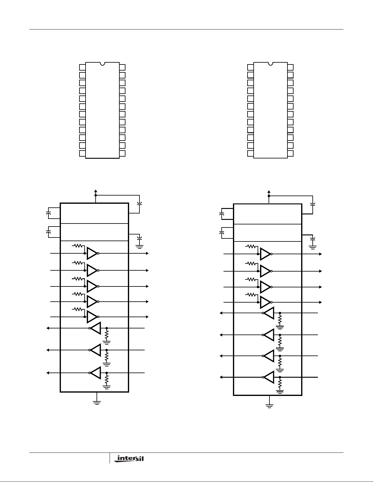
HIN232, HIN236, HIN237, HIN238, HIN239, HIN240, HIN241
HIN232 (PDIP, SOIC)
TOP VIEW
HIN236 (SOIC)
TOP VIEW
16
V
CC
15
GND
14
T1
OUT
13
R1
IN
12
R1
OUT
11
T1
IN
10
T2
IN
9
R2
OUT
T2
C1+
C2+
OUT
R2
V+
C1-
C2-
V-
1
2
3
4
5
6
7
8
IN
+5V
+
NOTE 1
NOTE 1
T1
T2
R1
OUT
R2
OUT
1µF
1
C1+
+
3
4
+
5
11
IN
10
IN
VOLTAGE DOUBL ER
C1C2+
VOLTAGE INVERTER
C2-
+5V
400kΩ
+5V
400kΩ
16
V
CC
+5V TO 10V
+10V TO -10V
T1
T2
R1
R2
5kΩ
5kΩ
V+
NOTE 1
+
2
6
V-
NOTE 1
+
14
7
1312
89
T1
T2
R1
R2
OUT
OUT
IN
IN
15
NOTE:
1. Either 0.1µF or 1µF capacitors may be used. The V+ capacitor
may be terminated to V
or to GND.
CC
R1
R2
R3
1
T3
OUT
2
T1
OUT
3
T2
OUT
4
R1
IN
OUT
T2
T1
GND
V
CC
C1+
V+
C1-
5
6
IN
7
IN
8
9
10
11
12
R1
+5V
10
C1+
+
1µF
12
C1-
13
C2+
+
1µF
14
T1
IN
T2
IN
18 1
T3
IN
19 24
T4
IN
OUT
VOLTAGE INVERTER
C2-
+5V
400kΩ
7
+5V
400kΩ
6
+5V
400kΩ
+5V
400kΩ
V
CC
+5V TO 10V
VOLTAGE DOUBL ER
+10V TO -10V
T1
T2
T3
T4
R1
OUT
R2
OUT
EN
20
R3
24
T4
OUT
23
R2
IN
22
R2
OUT
21
SD
20
EN
19
T4
IN
18
T3
IN
17
R3
OUT
16
R3
IN
15
V-
14
C2-
13
C2+
9
V+
V-
1µF
+
11
15
1µF
+
2
3
T1
OUT
T2
OUT
T3
OUT
T4
R1
OUT
IN
45
5kΩ
2322
R2
IN
5kΩ
1617
R3
5kΩ
21
IN
SD
8
4
Page 5
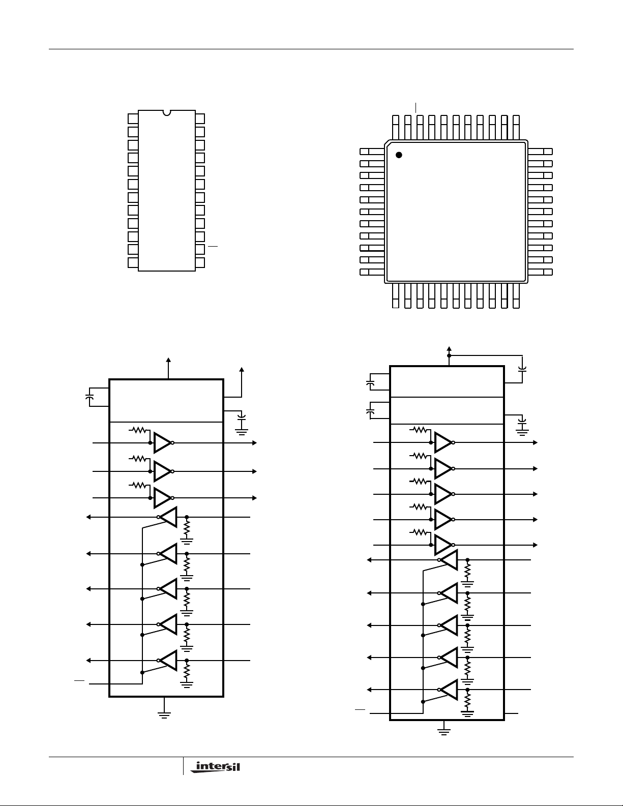
Pinouts (Continued)
HIN232, HIN236, HIN237, HIN238, HIN239, HIN240, HIN241
HIN237 (SOIC)
TOP VIEW
HIN238 (PDIP, SOIC)
TOP VIEW
R1
R2
R3
T3
1
OUT
T1
2
OUT
T2
3
OUT
R1
4
IN
R1
5
OUT
T2
6
IN
T1
7
IN
8
GND
V
9
CC
C1+
10
V+
11
C1-
12
+5V
10
C1+
+
1µF
12
C1-
13
C2+
+
1µF
14
C2-
+5V
400kΩ
T1
T2
T3
T4
T5
OUT
OUT
OUT
7
IN
+5V
400kΩ
6
IN
+5V
400kΩ
18 1
IN
+5V
400kΩ
19 24
IN
+5V
400kΩ
21 20
IN
V
+5V TO 10V
VOLTAGE DOUBLER
+10V TO -10V
VOLTAGE INVERTER
T1
T2
T3
T4
T5
R1
R2
R3
CC
T4
24
OUT
R2
23
IN
R2
22
OUT
T5
21
IN
T5
20
OUT
T4
19
IN
T3
18
IN
R3
17
OUT
R3
16
IN
V-
15
14
C2C2+
13
9
V+
V-
5kΩ
5kΩ
5kΩ
1µF
+
11
15
1µF
+
2
3
45
2322
1617
T1
T2
T3
T4
T5
R1
R2
R3
OUT
OUT
OUT
OUT
OUT
IN
IN
IN
R1
R2
R3
R4
1µF
1µF
T1
T2
T3
T4
OUT
OUT
OUT
OUT
T2
T1
R2
R1
10
+
12
13
+
14
5
IN
18
IN
19 24
IN
21 20
IN
1
OUT
2
OUT
R2
3
IN
4
OUT
T1
5
IN
6
OUT
R1
7
IN
GND
8
V
9
CC
C1+
10
V+
11
C1-
12
+5V
C1+
C1C2+
C2-
+5V
+5V
+5V
+5V
+5V TO 10V
VOLTAGE DOUBLER
+10V TO -10V
VOLTAGE INVERTER
400kΩ
400kΩ
400kΩ
400kΩ
T1
T2
T3
T4
V
R1
R2
R3
R4
9
CC
5kΩ
5kΩ
5kΩ
5kΩ
24
23
22
21
20
19
18
17
16
15
14
13
T3
R3
R3
T4
T4
T3
T2
R4
R4
VC2C2+
V+
V-
OUT
IN
OUT
IN
OUT
IN
IN
OUT
IN
11
15
2
1
76
34
2322
1617
+
+
1µF
1µF
T1
T2
T3
T4
R1
R2
R3
R4
OUT
OUT
OUT
OUT
IN
IN
IN
IN
8
8
5
Page 6
Pinouts (Continued)
HIN239 (PDIP, SOIC)
R1
1
OUT
R1
2
IN
3
GND
V
4
CC
5
V+
6
C1+
7
C1-
8
V-
R5
9
IN
R5
10
OUT
R4
11
OUT
R4
12
IN
HIN232, HIN236, HIN237, HIN238, HIN239, HIN240, HIN241
TOP VIEW
T1
24
IN
T2
23
IN
R2
22
OUT
R2
21
IN
T2
20
OUT
T1
19
OUT
R3
18
IN
R3
17
OUT
T3
16
IN
15
NC
14
EN
T3
13
OUT
R3
T4
T3
T1
T2
T5
R3
R2
NC
OUT
OUT
OUT
OUT
OUT
NC
NC
1
IN
2
3
IN
4
5
6
7
8
9
IN
10
11
12 13 14 15 16 17
HIN240 (MQFP)
OUT
R2
OUT
T5
IN
T2INT1
NCSDEN
44 43 42 41 40
NC
OUT
IN
R4
R4
39 38 37 36 35 34
IN
OUT
R1
R1
T4INT3INR5
CC
NCNCNC
V
GND
OUTR5IN
NC
33
32
31
30
29
28
27
26
25
24
23
2221201918
NC
NC
NC
VC2C2+
C1V+
C1+
NC
NC
+5V
4
1µF
(NOTE)
T1
T2
T3
R1
OUT
6
C1+
+
7
C1-
VOLTAGE INVERTER
+5V
400kΩ
24
IN
+5V
400kΩ
23
IN
+5V
400kΩ
16 13
IN
1
V
CC
+10V TO -10V
T1
T2
T3
R1
R2
OUT
R2
R3
OUT
R3
R4
OUT
R4
R5
OUT
R5
EN
14
3
NOTE: For V+ > 11V, use C1 ≤ 0.1µF.
+7.5V TO +13.2V (NOT E)
5
V+
8
V-
1µF
+
19
20
2
5kΩ
2122
5kΩ
1817
5kΩ
1211
5kΩ
910
5kΩ
T1
T2
T3
R1
R2
R3
R4
R5
OUT
OUT
OUT
IN
IN
IN
IN
IN
R1
R2
R3
R4
R5
1µF
1µF
T1
T2
T3
T4
T5
OUT
OUT
OUT
OUT
OUT
+5V
25
C1+
+
27
C1-
28
+
29
15
IN
14
IN
37 6
IN
38 5
IN
IN
VOLTAGE DOUBLER
C2+
VOLTAGE INVERTER
C2-
+5V
400kΩ
+5V
400kΩ
+5V
400kΩ
+5V
400kΩ
+5V
400kΩ
241
16
42
EN
19
V
CC
+5V TO 10V
+10V TO -10V
T1
T2
T3
T4
T5
R1
R2
R3
R4
R5
5kΩ
5kΩ
5kΩ
5kΩ
5kΩ
V+
V-
1µF
+
26
30
1µF
7
8
17
1013
43
4039
3536
43
SD
T1
T2
T3
T4
T5
R1
R2
R3
R4
R5
OUT
OUT
OUT
OUT
OUT
IN
IN
IN
IN
IN
18
6
Page 7

Pinouts (Continued)
HIN232, HIN236, HIN237, HIN238, HIN239, HIN240, HIN241
HIN241 (SOIC, SSOP)
TOP VIEW
28
T3
T1
T2
R2
R1
OUT
OUT
OUT
R2
OUT
T2
T1
OUT
R1
GND
V
CC
C1+
V+
C1-
1
2
3
4
IN
5
6
IN
7
IN
8
9
IN
10
11
12
13
14
T4
OUT
R3
27
IN
R3
26
OUT
SD
25
EN
24
R4
23
IN
R4
22
OUT
T4
21
IN
20
T3
IN
R5
19
OUT
R5
18
IN
V-
17
16
C2-
15
C2+
R1
R2
R3
R4
R5
1µF
1µF
T1
T2
T3
T4
OUT
OUT
OUT
OUT
OUT
+5V
12
C1+
+
14
C1-
15
+
16
IN
IN
20 1
IN
21 28
IN
8
VOLTAGE DOUBLER
C2+
VOLTAGE INVERTER
C2-
+5V
400kΩ
7
+5V
400kΩ
6
+5V
400kΩ
+5V
400kΩ
11
V
CC
+5V TO 10V
+10V TO -10V
T1
T2
T3
T4
R1
R2
R3
R4
R5
EN
24
10
5kΩ
5kΩ
5kΩ
5kΩ
5kΩ
V+
V-
1µF
+
13
17
1µF
+
2
3
9
45
2726
2322
1819
25
SD
T1
T2
T3
T4
R1
R2
R3
R4
R5
OUT
OUT
OUT
OUT
IN
IN
IN
IN
IN
7
Page 8

HIN232, HIN236, HIN237, HIN238, HIN239, HIN240, HIN241
Absolute Maximum Ratings Thermal Information
VCC to Ground. . . . . . . . . . . . . . . . . . . . . . (GND -0.3V) < VCC < 6V
V+ to Ground (Note 2) . . . . . . . . . . . . . . . (V
V- to Ground. . . . . . . . . . . . . . . . . . . . . . . .-12V < V- < (GND +0.3V)
-0.3V) < V+ < 13.2V
CC
V+ to V- . . . . . . . . . . . . . . . . . . . . . . . . . . . . . . . . . . . . . . . . . . . 24V
Input Voltages
T
. . . . . . . . . . . . . . . . . . . . . . . . . . . . . -0.3V < VIN < (V+ +0.3V)
IN
R
. . . . . . . . . . . . . . . . . . . . . . . . . . . . . . . . . . . . . . . . . . . . ±30V
IN
Output Voltages
T
. . . . . . . . . . . . . . . . . . . .(V- -0.3V) < V
OUT
R
. . . . . . . . . . . . . . . . . (GND -0.3V) < V
OUT
Short Circuit Duration
T
. . . . . . . . . . . . . . . . . . . . . . . . . . . . . . . . . . . . . .Continuous
OUT
R
. . . . . . . . . . . . . . . . . . . . . . . . . . . . . . . . . . . . . .Continuous
OUT
TXOUT
RXOUT
< (V+ +0.3V)
< (V+ +0.3V)
Thermal Resistance (Typical, Note 3) θ
16 Ld PDIP Package . . . . . . . . . . . . . . . . . . . . . . . . 90
24 Ld PDIP Package . . . . . . . . . . . . . . . . . . . . . . . . 70
16 Ld SOIC Package . . . . . . . . . . . . . . . . . . . . . . . . 100
24 Ld SOIC Package . . . . . . . . . . . . . . . . . . . . . . . . 75
28 Ld SOIC Package . . . . . . . . . . . . . . . . . . . . . . . . 70
28 Ld SSOP Package . . . . . . . . . . . . . . . . . . . . . . . 95
44 Ld MQFP Package . . . . . . . . . . . . . . . . . . . . . . . 80
Maximum Junction Temperature (Plastic Package) . . . . . . . .150
Maximum Storage Temperature Range. . . . . . . . . . -65
Maximum Lead Temperature (Soldering 10s) . . . . . . . . . . . . .300
(SOIC, SSOP, MQFP - Lead Tips Only)
Operating Conditions
Temperature Range
HIN2XXCX . . . . . . . . . . . . . . . . . . . . . . . . . . . . . . . . . 0
HIN2XXIX. . . . . . . . . . . . . . . . . . . . . . . . . . . . . . . . -40
CAUTION: Stresses above those listed in “Absolute Maximum Ratings” may cause permanent damage to the device. This is a stress only rating and operation of the
device at these or any other conditions above those indicated in the operational sections of this specification is not implied.
NOTE:
2. Only HIN239. For V+ > 11V, C1 must be ≤0.1µF.
is measured with the component mounted on a low effective thermal conductivity test board in free air. See Tech Brief TB379 for details.
3. θ
JA
o
C to 70oC
o
C to 85oC
(oC/W)
JA
o
C to 150oC
o
o
C
C
Electrical Specifications Test Conditions: V
= +5V ±10%, TA = Operating Temperature Range
CC
PARAMETER TEST CONDITIONS MIN TYP MAX UNITS
SUPPLY CURRENTS
Power Supply Current, I
CC
V+ Power Supply Current, I
No Load, TA = 25oC
Shutdown Supply Current, I
CC
(SD) TA = 25oC-110µA
CC
No Load,
T
= 25oC
A
No Load,
TA = 25oC
LOGIC AND TRANSMITTER INPUTS, RECEIVER OUTPUTS
Input Logic Low, V
Input Logic High, V
Transmitter Input Pullup Current, I
lL
lH
P
TTL/CMOS Receiver Output Voltage Low, V
TTL/CMOS Receiver Output Voltage High, V
TIN, EN, Shutdown - - 0.8 V
T
IN
, Shutdown 2.4 - - V
EN
TIN = 0V - 15 200 µA
I
OL
OH
= 1.6mA - 0.1 0.4 V
OUT
I
= -1.0mA 3.5 4.6 - V
OUT
RECEIVER INPUTS
RS-232 Input Voltage Range V
Receiver Input Impedance R
Receiver Input Low Threshold, V
Receiver Input High Threshold, V
Receiver Input Hysteresis V
IN
IN
(H-L) VCC = 5V, TA = 25oC0.81.2-V
lN
(L-H) VCC = 5V, TA = 25oC-1.72.4V
IN
HYST
VIN = ±3V 3.0 5.0 7.0 kΩ
HIN232 - 5 10 mA
HIN236-HIN238, HIN240-HIN241 - 7 15 mA
HIN239 - 0.4 1 mA
HIN239 - 5.0 15 mA
2.0 - - V
-30 - +30 V
0.2 0.5 1.0 V
8
Page 9

HIN232, HIN236, HIN237, HIN238, HIN239, HIN240, HIN241
Electrical Specifications Test Conditions: V
PARAMETER TEST CONDITIONS MIN TYP MAX UNITS
TIMING CHARACTERISTICS
Baud Rate (1 Transmitter Switching) R
Output Enable Time, t
Output Disable Time, t
Propagation Delay, t
Instantaneous Slew Rate SR C
Transition Region Slew Rate, SR
TRANSMITTER OUTPUTS
Output Voltage Swing, T
Output Resistance, T
RS-232 Output Short Circuit Current, I
NOTE:
4. Guaranteed by design.
V
CC
GND
EN
DIS
PD
OUT
OUT
VOLTAGE DOUBLER
S1
S3
T
SC
+
C1
C1-
S2
+
C1
-
S4
= +5V ±10%, TA = Operating Temperature Range (Continued)
CC
= 3kΩ 120 - - kbps
L
HIN236, HIN239, HIN240, HIN241 - 400 - ns
HIN236, HIN239, HIN240, HIN241 - 250 - ns
RS-232 to TTL - 0.5 - µs
= 10pF, RL = 3kΩ, TA = 25oC (Note 4) - - 30 V/µs
L
RL = 3kΩ, CL = 2500pF Measured from +3V to -3V or
-3-V/µs
-3V to +3V, 1 Transmitter Switching
Transmitter Outputs, 3kΩ to Ground ±5 ±9 ±10 V
VCC = V+ = V- = 0V, V
T
shorted to GND - ±10 - mA
OUT
+
C3
V
CC
= ±2V 300 - - Ω
OUT
VOLTAGE INVE RTER
V+ = 2V
GND
CC
S5
S7
C2
C2
+
S6
+
C2
-
-
S8
+
C4
-
GND
V- = -(V+)
RC
OSCILLATOR
FIGURE 1. CHARGE PUMP
Detailed Description
The HIN232 thru HIN241 family of RS-232
transmitters/receivers are powered by a single +5V pow er
supply (except HIN239), feature low power consumption, and
meet all ElA RS-232C and V.28 specifications. The circuit is
divided into three sections: The charge pump, transmitter, and
receiver.
Charge Pump
An equivalent circuit of the charge pump is illustrated in
Figure 1. The charge pump contains two sections: the v oltage
doubler and the voltag e in verter. Each section is drive n by a
two phase, internally generated clock to gener ate +10V and
-10V. The nominal clock frequency is 16kHz. During phase
one of the clock, capacitor C1 is charged to V
phase two, the voltage on C1 is added to V
signal across C3 equal to twice V
also charged to 2V
, and then during phase two, it is
CC
. During phase one, C2 is
CC
inverted with respect to ground to produce a signal across C4
equal to -2V
. The charge pump accepts input voltages up
CC
. During
CC
, producing a
CC
to 5.5V. The output impedance of the voltage doubler section
(V+) is approximately 200Ω, and the output impedance of the
voltage inv erter section (V-) is approximately 450Ω. A typical
application uses 1µF capacitors for C1-C4, ho we ver , the val ue
is not critical. Increasing the values of C1 and C2 will lo wer the
output impedance of the voltage doubler an d inverter,
increasing the values of the reservoir capacitors, C3 and C4,
lowers the ripple on the V+ and V- supplies.
During shutdown mode (HIN236, HIN240 and HIN241),
SHUTDOWN control line set to logic “1”, the charge pump is
turned off, V+ is pulled down to V
, V - is pulled up to GND,
CC
and the supply current is reduced to less than 10µA. The
transmitter outputs are disabled and the receiver outputs are
placed in the high impedance state.
9
Page 10

HIN232, HIN236, HIN237, HIN238, HIN239, HIN240, HIN241
Transmitters
The transmitters are TTL/CMOS compatible inverters which
translate the inputs to RS-232 outputs. The input logic threshold
is about 26% of V
input results in a voltage of between -5V and V- at the output,
and a logic 0 results in a voltage between +5V and (V+ -0.6V).
Each transmitter input has an internal 400kΩ pullup resistor so
any unused input can be left unconnected and its output
remains in its low state. The output voltage swing meets the
RS-232C specifications of ±5V minimum with the worst case
conditions of: all transmitters driving 3kΩ minimum load
impedance, V
temperature. The transmitters have an internally limited output
slew rate which is less than 30V/µs. The outputs are short
circuit protected and can be shorted to ground indefinitely. The
powered down output impedance is a minimum of 300Ω with
±2V applied to the outputs and V
V+
V
CC
T
XIN
GND < T
XIN
, or 1.3V for VCC = 5V. A logic 1 at the
CC
= 4.5V, and maximum allowable operating
CC
= 0V.
CC
< V
400kΩ
CC
300Ω
V- < V
T
OUT
TOUT
< V+
Receivers
The receiver inputs accept up to ±30V while presenting the
required 3kΩ to 7kΩ input impedance even if the power is off
(V
= 0V). The receivers have a typical input threshold of
CC
1.3V which is within the ±3V limits, known as the transition
region, of the RS-232 specifications. The receiver output is
0V to V
greater than 2.4V and high whenever the input is floating or
driven between +0.8V and -30V. The receivers feature 0.5V
hysteresis to improve noise rejection. The receiver Enable
line EN
disables the receiver outputs, placing them in the high
impedance mode. The receiver outputs are also placed in
the high impedance state when in shutdown mode.
. The output will be low whenever the input is
CC
, when set to logic “1”, (HIN236, 239, 240, and 241)
V
CC
R
-30V < R
XIN
< +30V
XIN
GND
5kΩ
FIGURE 3. RECEIVER
GND < V
R
OUT
ROUT
< V
CC
V-
FIGURE 2. TRANSMITTER
T
IN
OR
R
IN
T
OUT
OR
R
OUT
t
PHL
Average Propagation Delay =
t
PLH
t
PHL + tPLH
2
FIGURE 4. PROPAGATION DELAY DEFINITION
V
OL
V
OL
10
Page 11

HIN232, HIN236, HIN237, HIN238, HIN239, HIN240, HIN241
Typical Performance Curves
12
10
8
6
4
V- SUPPLY VOLTAGE
2
1µF
0.47µF
0.10µF
TA = 25oC
12
TRANSMITTER OUTPUTS
OPEN CIRCUIT
10
8
6
V- (VCC = 4.5V)
4
SUPPLY VOLTAGE (|V|)
2
V+ (VCC = 5V)
V+ (VCC = 4.5V)
V- (VCC = 5V)
0
3.0
3.5
4.0 4.5 6.0
V
CC
5.0 5.5
FIGURE 5. V- SUPPLY V OLTA GE vs VCC, VARYING
CAPACITORS
Test Circuits (HIN232)
-
1µF
C3
1µF
C1
1µF
C2
3kΩ
T2
OUTPUT
RS-232
±30V INPUT
+
+
-
+
-
+
1µF C4
C1+
1
V+
2
C1-
3
C2+
4
C2-
5
-
V-
6
T2
7
8
R2
OUT
IN
T1
R1
R2
V
CC
GND
OUT
R1
OUT
T1
T2
OUT
16
15
14
RS-232 ±30V INPUT
13
IN
TTL/CMOS OUTPUT
12
TTL/CMOS INPUT
11
IN
TTL/CMOS INPUT
10
IN
TTL/CMOS OUTPUT
9
+4.5V TO
+5.5V INPUT
3kΩ
T1 OUTPUT
0
0
|I
LOAD
| (mA)
30252015105
FIGURE 6. V+, V- OUTPUT VOLTAGE vs LOAD (HIN232)
1
2
3
4
5
6
7
8
R
OUT
VIN = ±2V
C1+
V+
C1C2+
C2V-
T2
OUT
R2
IN
= VIN/1
T1
R1
R2
T2
V
CC
GND
OUT
R1
OUT
T1
T2
OUT
OUT
T1
16
15
14
13
IN
12
11
IN
10
IN
9
OUT
A
35
FIGURE 7. GENERAL TEST CIRCUIT
11
FIGURE 8. POWER-OFF SOURCE RESIST ANCE
CONFIGURATION
Page 12

HIN232, HIN236, HIN237, HIN238, HIN239, HIN240, HIN241
Applications
The HIN2XX may be used for all RS-232 data terminal and
communication links. It is particularly useful in applications
where ±12V power supplies are not available for
conventional RS-232 interface circuits. The applications
presented represent typical interface configurations.
A simple duplex RS-232 port with CTS/RTS handshaking is
illustrated in Figure 9. Fixed output signals such as DTR
(data terminal ready) and DSRS (data signaling rate select)
is generated by driving them through a 5kΩ resistor
connected to V+.
In applications requiring four RS-232 inputs and outputs
(Figure 10), note that each circuit requires two charge pump
capacitors (C1 and C2) but can share common reservoir
capacitors (C3 and C4). The benefit of sharing common
reservoir capacitors is the elimination of two capacitors and
the reduction of the charge pump source impedance which
effectively increases the output swing of the transmitters.
1
+
TTL/CMOS
INPUTS AND
OUTPUTS
C1
1µF
-
TD
RTS
RD
CTS
HIN232
3
T1
11
R2
T2
R1
10
12
9
TTL/CMOS
INPUTS AND
OUTPUTS
FIGURE 9. SIMPLE DUPLEX RS-232 PORT WITH CTS/RTS
4
+
C2
5
1µF
-
14
TD (2) TRANSMIT DATA
7
RTS (4) REQUEST TO SEND
13
RD (3) RECEIVE DATA
8
CTS (5) CLEAR TO SEND
15
+5V
1
+
C1
3
1µF
-
4
+
C2
5
1µF
-
11
TD
10
RTS
12
RD
R2
9
CTS
HANDSHAKING
16
HIN232
T1
R1
T2
-
+
DTR (20) DATA
2
6
-
+
14
TD (2) TRANSMIT DATA
7
RTS (4) REQUEST TO SEND
13
RD (3) RECEIVE DATA
8
CTS (5) CLEAR TO SEND
SIGNAL GROUND (7)15
TERMINAL READY
DSRS (24) DATA
SIGNALING RATE
SELECT
RS-232
INPUTS AND OUTPUTS
16
TTL/CMOS
INPUTS AND
OUTPUTS
2µF
C1
1µF
DTR
DSRS
DCD
R1
26
C4
+
-
V- V+
6
HIN232
1
+
3
-
T1
11
R2
T2
R1
10
12
9
C3
+
2µF
2
16
4
+
C2
5
1µF
-
14
DTR (20) DATA TERMINAL READY
7
DSRS (24) DATA SIGNALING RATE SELECT
13
DCD (8) DATA CARRIER DETECT
8
R1 (22) RING INDICATOR
SIGNAL GROUND (7)15
+5V
-
RS-232
INPUTS AND OUTPUTS
FIGURE 10. COMBINING TWO HIN232s FOR 4 PAIRS OF RS-232 INPUTS AND OUTPUTS
12
Page 13

HIN232, HIN236, HIN237, HIN238, HIN239, HIN240, HIN241
Die Characteristics
DIE DIMENSIONS
160 mils x 140 mils
METALLIZATION
Type: Al
Thickness: 10k
Å ±1kÅ
SUBSTRATE POTENTIAL
V+
Metallization Mask Layout
R2
IN
R2
OUT
T2
IN
T2
OUT
T1
OUT
T3
OUT
HIN240
T4
OUT
PASSIVATION
Type: Nitride over Silox
Nitride Thickness: 8k
Silox Thickness: 7kÅ
TRANSISTOR COUNT
238
PROCESS
CMOS Metal Gate
R3
IN
R3
OUT
Å
T5
IN
SHUTDOWN
EN
R1
T1
OUT
R1
GND
V
CC
T5
R4
R4
T4
T3
R5
R5
OUT
IN
OUT
IN
IN
OUT
IN
IN
IN
13
C1+ V+ C1-
V-C2-C2+
Page 14

HIN232, HIN236, HIN237, HIN238, HIN239, HIN240, HIN241
Dual-In-Line Plastic Packages (PDIP)
N
D1
-C-
E1
-B-
A1
A2
E
A
L
e
C
C
L
e
A
C
e
B
INDEX
AREA
BASE
PLANE
SEATING
PLANE
D1
B1
12 3 N/2
-AD
e
B
0.010 (0.25) C AM BS
NOTES:
1. Controlling Dimensions: INCH. In case of conflict between English and
Metric dimensions, the inch dimensions control.
2. Dimensioning and tolerancing per ANSI Y14.5M-1982.
3. Symbols are defined in the “MO Series Symbol List” in Section 2.2 of
Publication No. 95.
4. Dimensions A, A1 and L are measured with the package seated in JEDEC seating plane gauge GS-3.
5. D, D1, and E1 dimensions do not include mold flash or protrusions.
Mold flash or protrusions shall not exceed 0.010 inch (0.25mm).
6. E and are measured with the leads constrained to be perpendic-
7. e
e
A
ular to datum .
and eC are measured at the lead tips with the leads unconstrained.
B
e
must be zero or greater.
C
-C-
8. B1 maximum dimensions do not include dambar protrusions. Dambar
protrusions shall not exceed 0.010 inch (0.25mm).
9. N is the maximum number of terminal positions.
10. Corner leads (1, N, N/2 and N/2 + 1) for E8.3, E16.3, E18.3, E28.3,
E42.6 will have a B1 dimension of 0.030 - 0.045 inch (0.76 - 1.14mm).
E16.3 (JEDEC MS-001-BB ISSUE D)
16 LEAD DUAL-IN-LINE PLASTIC PACKAGE
INCHES MILLIMETERS
SYMBOL
A - 0.210 - 5.33 4
A1 0.015 - 0.39 - 4
A2 0.115 0.195 2.93 4.95 -
B 0.014 0.022 0.356 0.558 B1 0.045 0.070 1.15 1.77 8, 10
C 0.008 0.014 0.204 0.355 -
D 0.735 0.775 18.66 19.68 5
D1 0.005 - 0.13 - 5
E 0.300 0.325 7.62 8.25 6
E1 0.240 0.280 6.10 7.11 5
e 0.100 BSC 2.54 BSC e
A
e
B
0.300 BSC 7.62 BSC 6
- 0.430 - 10.92 7
L 0.115 0.150 2.93 3.81 4
N16 169
NOTESMIN MAX MIN MAX
Rev. 0 12/93
14
Page 15

HIN232, HIN236, HIN237, HIN238, HIN239, HIN240, HIN241
Dual-In-Line Plastic Packages (PDIP)
N
D1
-C-
E1
-B-
A1
A2
E
A
L
e
C
C
L
e
A
C
e
B
INDEX
AREA
BASE
PLANE
SEATING
PLANE
D1
B1
12 3 N/2
-AD
e
B
0.010 (0.25) C AM BS
NOTES:
1. Controlling Dimensions: INCH. In case of conflict between English and
Metric dimensions, the inch dimensions control.
2. Dimensioning and tolerancing per ANSI Y14.5M-1982.
3. Symbols are defined in the “MO Series Symbol List” in Section 2.2 of
Publication No. 95.
4. Dimensions A, A1 and L are measured with the package seated in
JEDEC seating plane gauge GS-3.
5. D, D1, and E1 dimensions do not include mold flash or protrusions.
Mold flash or protrusions shall not exceed 0.010 inch (0.25mm).
6. E and are measured with the leads constrained to be perpendic-
7. e
e
A
ular to datum .
and eC are measured at the lead tips with the leads unconstrained.
B
e
must be zero or greater.
C
-C-
8. B1 maximum dimensions do not include dambar protrusions. Dambar
protrusions shall not exceed 0.010 inch (0.25mm).
9. N is the maximum number of terminal positions.
10. Corner leads (1, N, N/2 and N/2 + 1) for E8.3, E16.3, E18.3, E28.3,
E42.6 will have a B1 dimension of 0.030 - 0.045 inch (0.76 - 1.14mm).
E24.3 (JEDEC MS-001-AF ISSUE D)
24 LEAD NARROW BODY DUAL-IN-LINE PLASTIC
PACKAGE
INCHES MILLIMETERS
SYMBOL
A - 0.210 - 5.33 4
A1 0.015 - 0.39 - 4
A2 0.115 0.195 2.93 4.95 -
B 0.014 0.022 0.356 0.558 B1 0.045 0.070 1.15 1.77 8
C 0.008 0.014 0.204 0.355 -
D 1.230 1.280 31.24 32.51 5
D1 0.005 - 0.13 - 5
E 0.300 0.325 7.62 8.25 6
E1 0.240 0.280 6.10 7.11 5
e 0.100 BSC 2.54 BSC e
A
e
B
0.300 BSC 7.62 BSC 6
- 0.430 - 10.92 7
L 0.115 0.150 2.93 3.81 4
N24 249
NOTESMIN MAX MIN MAX
Rev. 0 12/93
15
Page 16

HIN232, HIN236, HIN237, HIN238, HIN239, HIN240, HIN241
Small Outline Plastic Packages (SOIC)
N
INDEX
AREA
123
SEA TING PLANE
-AD
e
B
0.25(0.010) C AM BS
M
E
-B-
A
-C-
0.25(0.010) BM M
H
α
µ
A1
0.10(0.004)
L
h x 45
o
C
NOTES:
1. Symbols are defined in the “MO Series Symbol List” in Section 2.2 of
Publication Number 95.
2. Dimensioning and tolerancing per ANSI Y14.5M-1982.
3. Dimension “D” does not include mold flash, protrusions or gate burrs.
Mold flash, protrusion and gate burrs shall not exceed 0.15mm (0.006
inch) per side.
4. Dimension “E” does not include interlead flash or protrusions. Interlead
flash and protrusions shall not exceed 0.25mm (0.010 inch) per side.
5. The chamfer on the body is optional. If it is not present, a visual index
feature must be located within the crosshatched area.
6. “L” is the length of terminal for soldering to a substrate.
7. “N” is the number of terminal positions.
8. Terminal numbers are shown for reference only.
9. The lead width “B”, as measured 0.36mm (0.014 inch) or greater above
the seating plane, shall not exceed a maximum value of 0.61mm (0.024
inch)
10. Controlling dimension: MILLIMETER. Converted inch dimensions are
not necessarily exact.
M16.3 (JEDEC MS-013-AA ISSUE C)
16 LEAD WIDE BODY SMALL OUTLINE PLASTIC PACKAGE
INCHES MILLIMETERS
SYMBOL
A 0.0926 0.1043 2.35 2.65 -
A1 0.0040 0.0118 0.10 0.30 -
B 0.013 0.0200 0.33 0.51 9
C 0.0091 0.0125 0.23 0.32 D 0.3977 0.4133 10.10 10.50 3
E 0.2914 0.2992 7.40 7.60 4
e 0.050 BSC 1.27 BSC H 0.394 0.419 10.00 10.65 -
h 0.010 0.029 0.25 0.75 5
L 0.016 0.050 0.40 1.27 6
N16 167
o
α
0
o
8
o
0
o
8
Rev. 0 12/93
NOTESMIN MAX MIN MAX
-
16
Page 17

HIN232, HIN236, HIN237, HIN238, HIN239, HIN240, HIN241
Small Outline Plastic Packages (SOIC)
N
INDEX
AREA
123
SEA TING PLANE
-AD
e
B
0.25(0.010) C AM BS
M
E
-B-
A
-C-
0.25(0.010) BM M
H
α
µ
A1
0.10(0.004)
L
h x 45
o
C
NOTES:
1. Symbols are defined in the “MO Series Symbol List” in Section 2.2 of
Publication Number 95.
2. Dimensioning and tolerancing per ANSI Y14.5M-1982.
3. Dimension “D” does not include mold flash, protrusions or gate burrs.
Mold flash, protrusion and gate burrs shall not exceed 0.15mm
(0.006 inch) per side.
4. Dimension “E” does not include interlead flash or protrusions. Interlead flash and protrusions shall not exceed 0.25mm (0.010 inch) per
side.
5. The chamfer on the body is optional. If it is not present, a visual index
feature must be located within the crosshatched area.
6. “L” is the length of terminal for soldering to a substrate.
7. “N” is the number of terminal positions.
8. Terminal numbers are shown for reference only.
9. The lead width “B”, as measured 0.36mm (0.014 inch) or greater
above the seating plane, shall not exceed a maximum value of
0.61mm (0.024 inch)
10. Controlling dimension: MILLIMETER. Converted inch dimensions
are not necessarily exact.
M24.3 (JEDEC MS-013-AD ISSUE C)
24 LEAD WIDE BODY SMALL OUTLINE PLASTIC PACKAGE
INCHES MILLIMETERS
SYMBOL
A 0.0926 0.1043 2.35 2.65 -
A1 0.0040 0.0118 0.10 0.30 -
B 0.013 0.020 0.33 0.51 9
C 0.0091 0.0125 0.23 0.32 D 0.5985 0.6141 15.20 15.60 3
E 0.2914 0.2992 7.40 7.60 4
e 0.05 BSC 1.27 BSC -
H 0.394 0.419 10.00 10.65 -
h 0.010 0.029 0.25 0.75 5
L 0.016 0.050 0.40 1.27 6
N24 247
o
α
0
o
8
o
0
o
8
Rev. 0 12/93
NOTESMIN MAX MIN MAX
-
17
Page 18

HIN232, HIN236, HIN237, HIN238, HIN239, HIN240, HIN241
Small Outline Plastic Packages (SOIC)
N
INDEX
AREA
123
SEA TING PLANE
-AD
e
B
0.25(0.010) C AM BS
M
E
-B-
A
-C-
0.25(0.010) BM M
H
α
µ
A1
0.10(0.004)
L
h x 45
o
NOTES:
1. Symbols are defined in the “MO Series Symbol List” in Section 2.2
of Publication Number 95.
2. Dimensioning and tolerancing per ANSI Y14.5M-1982.
3. Dimension “D” does not include mold flash, protrusions or gate
burrs. Mold flash, protrusion and gate burrs shall not exceed
0.15mm (0.006 inch) per side.
4. Dimension “E” does not include interlead flash or protrusions. Interlead flash and protrusions shall not exceed 0.25mm (0.010
inch) per side.
5. The chamfer on the body is optional. If it is not present, a visual
index feature must be located within the crosshatched area.
6. “L” is the length of terminal for soldering to a substrate.
7. “N” is the number of terminal positions.
8. Terminal numbers are shown for reference only.
9. The lead width “B”, as measured 0.36mm (0.014 inch) or greater
above the seating plane, shall not exceed a maximum value of
0.61mm (0.024 inch)
10. Controlling dimension: MILLIMETER. Converted inch dimensions are not necessarily exact.
M28.3 (JEDEC MS-013-AE ISSUE C)
28 LEAD WIDE BODY SMALL OUTLINE PLASTIC PACKAGE
INCHES MILLIMETERS
SYMBOL
A 0.0926 0.1043 2.35 2.65 -
A1 0.0040 0.0118 0.10 0.30 -
B 0.013 0.0200 0.33 0.51 9
C 0.0091 0.0125 0.23 0.32 D 0.6969 0.7125 17.70 18.10 3
E 0.2914 0.2992 7.40 7.60 4
e 0.05 BSC 1.27 BSC H 0.394 0.419 10.00 10.65 -
C
h 0.01 0.029 0.25 0.75 5
L 0.016 0.050 0.40 1.27 6
N28 287
o
α
0
o
8
o
0
o
8
Rev. 0 12/93
NOTESMIN MAX MIN MAX
-
18
Page 19

HIN232, HIN236, HIN237, HIN238, HIN239, HIN240, HIN241
Shrink Small Outline Plastic Packages (SSOP)
N
INDEX
AREA
123
SEATING PLANE
-AD
e
B
0.25(0.010) C AM BS
M
E
-B-
A
-C-
0.25(0.010) BM M
H
α
µ
A1
0.10(0.004)
GAUGE
PLANE
0.25
0.010
A2
L
C
NOTES:
1. Symbols are defined in the “MO Series Symbol List” in Section 2.2
of Publication Number 95.
2. Dimensioning and tolerancing per ANSI Y14.5M-1982.
3. Dimension “D” does not include mold flash, protrusions or gate
burrs. Mold flash, protrusion and gate burrs shall not exceed
0.20mm (0.0078 inch) per side.
4. Dimension “E” does not include interlead flash or protrusions. Interlead flash and protrusions shall not exceed 0.20mm (0.0078 inch)
per side.
5. The chamfer on the body is optional. If it is not present, a visual index feature must be located within the crosshatched area.
6. “L” is the length of terminal for soldering to a substrate.
7. “N” is the number of terminal positions.
8. Terminal numbers are shown for reference only.
9. Dimension “B” does not include dambar protrusion. Allowable dambar protrusion shall be 0.13mm (0.005 inch) total in excess of “B”
dimension at maximum material condition.
10. Controlling dimension: MILLIMETER. Converted inch dimensions
are not necessarily exact.
M28.209 (JEDEC MO-150-AH ISSUE B)
28 LEAD SHRINK SMALL OUTLINE PLASTIC PACKAGE
INCHES MILLIMETERS
SYMBOL
A - 0.078 - 2.00 A1 0.002 - 0.05 - A2 0.065 0.072 1.65 1.85 -
B 0.009 0.014 0.22 0.38 9
C 0.004 0.009 0.09 0.25 -
D 0.390 0.413 9.90 10.50 3
E 0.197 0.220 5.00 5.60 4
e 0.026 BSC 0.65 BSC -
H 0.292 0.322 7.40 8.20 -
L 0.022 0.037 0.55 0.95 6
N28 287
o
α
0
o
8
o
0
o
8
Rev. 1 3/95
NOTESMIN MAX MIN MAX
-
19
Page 20

HIN232, HIN236, HIN237, HIN238, HIN239, HIN240, HIN241
Metric Plastic Quad Flatpack Packages (MQFP)
E
E1
0.40
0.016
0o MIN
0o-7
-H-
-A-
o
MIN
D
D1
-D-
Q44.10x10 (JEDEC MS-022AB ISSUE B)
44 LEAD METRIC PLASTIC QUAD FLATPACK PACKAGE
INCHES MILLIMETERS
SYMBOL
NOTESMIN MAX MIN MAX
A - 0.096 - 2.45 -
A1 0.004 0.010 0.10 0.25 -
-B-
A2 0.077 0.083 1.95 2.10 -
b 0.012 0.018 0.30 0.45 6
b1 0.012 0.016 0.30 0.40 -
D 0.515 0.524 13.08 13.32 3
D1 0.389 0.399 9.88 10.12 4, 5
E 0.516 0.523 13.10 13.30 3
e
PIN 1
E1 0.390 0.398 9.90 10.10 4, 5
L 0.029 0.040 0.73 1.03 N44 447
e 0.032 BSC 0.80 BSC -
12o-16
A2
SEATING
PLANE
A
0.076
o
A1
0.20
0.008
A-B SD SCM
0.003
-C-
b
b1
NOTES:
1. Controlling dimension: MILLIMETER. Converted inch
dimensions are not necessarily exact.
2. All dimensions and tolerances per ANSI Y14.5M-1982.
3. Dimensions D and E to be determined at seating plane .
4. Dimensions D1 and E1 to be determined at datum plane
.
-H-
5. Dimensions D1 and E1 do not include mold protrusion.
Rev. 2 4/99
-C-
Allowable protrusion is 0.25mm (0.010 inch) per side.
0.13/0.17
o
L
12o-16
0.005/0.007
BASE METAL
WITH PLATING
0.13/0.23
0.005/0.009
6. Dimension b does not include dambar protrusion. Allowable
dambar protrusion shall be 0.08mm (0.003 inch) total.
7. “N” is the number of terminal positions.
All Intersil products are manufactured, assembled and tested utilizing ISO9000 quality systems .
Intersil Corporation’s quality certifications can be viewed at website www.intersil.com/quality/iso.asp
Intersil products are sold by description only. Intersil Corporation reserves the right to make changes in circuit design and/or specifications at any time without notice.
Accordingly, the reader is cautioned to verify that data sheets are current before pla cing orders . Inf ormation furnished b y Intersil is belie v ed to be accurate and re liabl e. However , no responsib ility is assumed by In tersil or its subsidia ries f or its use; nor f or any i nfringements of patents or other rights of third p arties which may resu lt from its use . No
license is granted by implication or otherwise under any patent or patent rights of Intersil or its subsidiaries.
.
For information regarding Intersil Corporation and its products, see web site www.intersil.com
20
 Loading...