HI-DAC80V,
HI-DAC85V
August 1997
Features
• DAC 80V/DAC 85V Alternative Source
• Monolithic Construction
• Fast Settling Time (Typ) . . . . . . . . . . . . . . . . . . . . 1.5µs
• Guaranteed Monotonicity
• Wafer Laser Trimmed Linearity, Gain, Offset
• Span Resistors On-Chip
• On-Board Reference
• Supply Operation. . . . . . . . . . . . . . . . . . . . . . . . . . ±12V
Applications
• High Speed A/D Converters
• Precision Instrumentation
• CRT Display Generation
Ordering Information
TEMP.
PART NUMBER
HI3-DAC80V-5 0 to 75 24 Ld PDIP E24.6
HI3-DAC85V-4 -25 to 85 24 Ld PDIP E24.6
RANGE (oC) PACKAGE
12-Bit, Low Cost, Monolithic D/A Converters
Description
The Hl-DAC80V is a monolithic direct replacement for the
popular DAC80 and AD DAC80. The HI-DAC85V is a monolithic direct replacement for the popular DAC85 and AD
DAC85 as well as the HI-5685V. Single chip construction
along with several design innovations make the Hl-DAC80V
the optimum choice for low cost, high reliability applications.
Intersil’ unique Dielectric Isolation (Dl) processing reduces
internal parasitics resulting in fast switching times and minimum glitch. On board span resistors are provided for good
tracking over temperature, and are laser trimmed to high
accuracy.
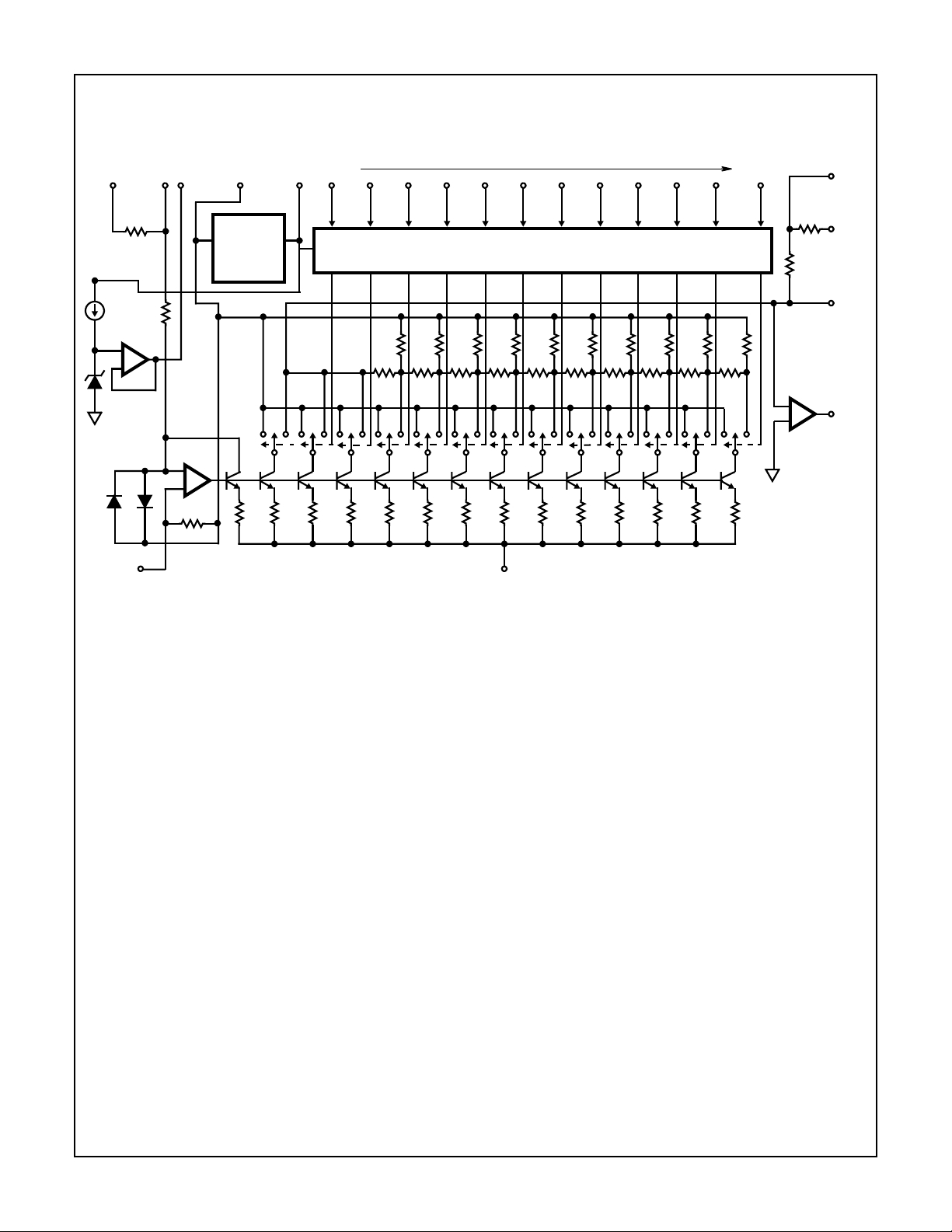
Internally the Hl-DAC80V/HI-DAC85V eliminates code
dependent ground currents by routing current from the positive supply to the internal ground node, as determined by an
auxiliary R2R ladder. This results in a cancellation of code
dependent ground currents allowing virtually zero variation
in current through the package common, pin 21.
PKG.
NO.
The Hl-DAC80V is available as a voltage output device which
is guaranteed over the 0
HI-DAC85V is available as a voltage output device which is
guaranteed over the -25
includes a buried zener reference featuring a low temperature
coefficient as well as an on board operational amplifier. The
Hl-DAC80V requires only two power supplies and will operate
in the range of ± (11.4V to 16.5V).
o
C to 75oC temperature range. The
o
C to 85oC temperature range. It
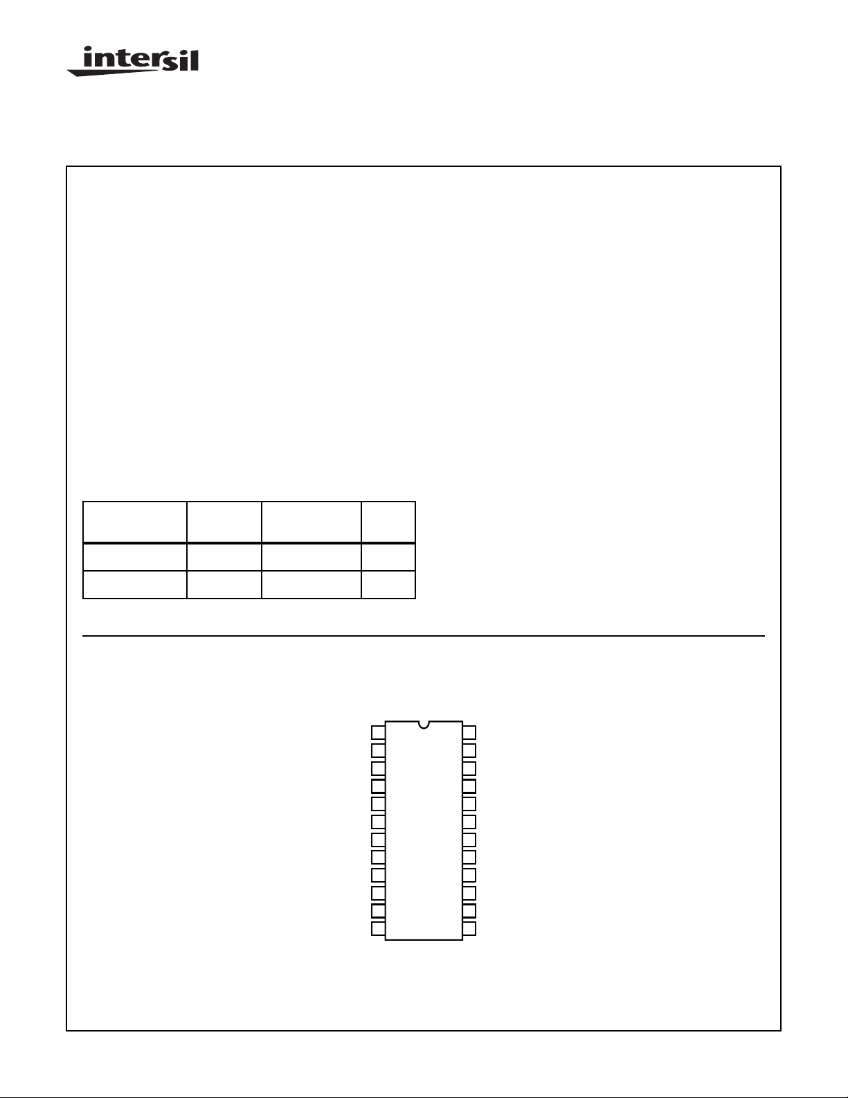
Pinout
HI-DAC80V/HI-DAC85V
(PDIP)
TOP VIEW
(MSB) BIT 1
(LSB) BIT 12
CAUTION: These devices are sensitive to electrostatic discharge; follow proper IC Handling Procedures.
http://www.intersil.com or 407-727-9207
| Copyright © Intersil Corporation 1999
BIT 2
BIT 3
BIT 4
BIT 5
BIT 6
BIT 7
BIT 8
BIT 9
BIT 10
BIT 11
1
2
3
4
5
6
7
8
9
10
11
12
10-1034
24
6.3V REF OUT
GAIN ADJUST
23
+V
22
S
21
COMMON
∑ JUNCTION
20
19
20V RANGE
10V RANGE
18
17
BIPOLAR OFFSET
REF INPUT
16
15
V
OUT
14
-V
S
13
NC
File Number 3110.1

Functional Block Diagram
HI-DAC80V, HI-DAC85V
BIPOLAR
OFFSET
6.3K
12.6K
+
-
CONTROL
AMP
GAIN
ADJUST
REF
OUT COMMON
IN
+
-
12.6K
GROUND
CURRENT
CANCEL-
LATION
CIRCUIT
8K
+V
S
BIT 1 IN
(MSB)
DIGITAL INPUT LEVEL SHIFTERS AND SWITCH DRIVERS
2K
2K
2K
2K
2K
2K
2K
1K
1K
1K
1K
1K
1K
1K
8K
8K
8K
8K
8K
8K
8K8K8K
-V
S
8K
1K
2K
8K
1K
2K
8K
BIT 12 IN
1K
1K
(LSB)
8K
5K
5K
SPAN Σ
JUNCTION
-
+
10V
SPAN R
20V
SPAN R
V
OUT
10-1035

HI-DAC80V, HI-DAC85V
Absolute Maximum Ratings Thermal Information
Power Supply Inputs
+VS. . . . . . . . . . . . . . . . . . . . . . . . . . . . . . . . . . . . . . . . . . . . +20V
-VS . . . . . . . . . . . . . . . . . . . . . . . . . . . . . . . . . . . . . . . . . . . . .-20V
Reference
Input (Pin 16) . . . . . . . . . . . . . . . . . . . . . . . . . . . . . . . . . . . . . +V
Output Drain . . . . . . . . . . . . . . . . . . . . . . . . . . . . . . . . . . . . 2.5mA
Digital Inputs (Bits 1 to 12) . . . . . . . . . . . . . . . . . . . . . . . .-1V to +V
Operating Conditions
Operating Temperature Range
HI-DAC80V. . . . . . . . . . . . . . . . . . . . . . . . . . . . . . . . .0oC to 75oC
HI-DAV85V . . . . . . . . . . . . . . . . . . . . . . . . . . . . . . . -25oC to 85oC
CAUTION: Stresses above those listed in “Absolute Maximum Ratings” may cause permanent damage to the device. This is a stress only rating and operation
of the device at these or any other conditions above those indicated in the operational sections of this specification is not implied.
NOTE:
1. θJA is measured with the component mounted on an evaluation PC board in free air.
Thermal Resistance (Typical, Note 1) θJA (oC/W)
PDIP Package. . . . . . . . . . . . . . . . . . . . . . . . . . . . . 60
Maximum Power Dissipation
PDIP Package. . . . . . . . . . . . . . . . . . . . . . . . . . . . . . . . . . 550mW
S
Maximum Junction Temperature . . . . . . . . . . . . . . . . . . . . . . .150oC
Maximum Storage Temperature Range . . . . . . . . . .-65oC to 150oC
S
Maximum Lead Temperature (Soldering 10s). . . . . . . . . . . . . 300oC
Die Characteristics
Process. . . . . . . . . . . . . . . . . . . . . . . . . . . . . . . . . . . . . . . Bipolar-DI
Transistor Count . . . . . . . . . . . . . . . . . . . . . . . . . . . . . . . . . . . . . 214
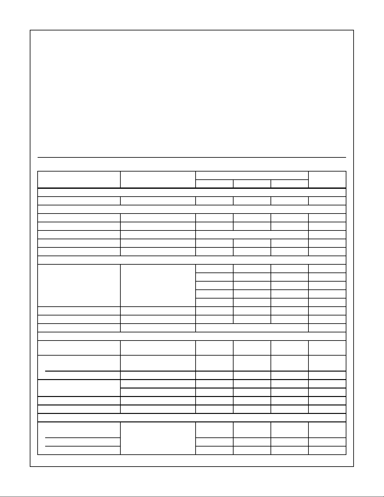
Electrical Specifications T
PARAMETER TEST CONDITIONS
SYSTEM PERFORMANCE
Resolution - - 12 Bits
ACCURACY (Note 2)
Linear Error Full Temperature - ±
Differential Linearity Error Full Temperature - ±1/
Monotonicity Full Temperature Guaranteed
Gain Error Full Temperature (Notes 1, 3) - ±0.1 ±0.3 % FSR
Offset Error Full Temperature (Note 1) ±0.05 ±0.15 % FSR
ANALOG OUTPUT
Output Ranges - ±2.5 - V
Output Current ±5- -mA
Output Resistance - 0.05 - Ω
Short Circuit Duration To Common Continuous DRIFT (Note 2)
Total Bipolar Drift (Includes Gain,
Offset and Linearity Drifts)
Total Error
Unipolar Full Temperature (Note 5) - ±0.08 ±0.15 % FSR
Bipolar Full Temperature (Note 5) - ±0.06 ±0.1 % FSR
Gain With Internal Reference - ±15 ±30 ppm/
Unipolar Offset - ±1 ±3 ppm/oC
Bipolar Offset - ±5 ±10 ppm/oC
CONVERSION SPEED
Settling Time Full Scale Transition All Bits ON
With 10K Feedback - 3 - µs
With 5K Feedback - 1.5 - µs
For 1 LSB Change - 1.5 - µs
= 25oC, VS ±12V to ±15V (Note 4), Pin 16 to Pin 24, Unless Otherwise Specified
A
HI-DAC80V-5, HI-DAC85V-5
UNITSMIN TYP MAX
1
/
4
2
- ±5- V
- ±10 - V
- 0 to 5 - V
- 0 to 10 - V
Full Temperature - - ±20 ppm/oC
Without Internal Reference - ±7 - ppm/oC
to OFF or OFF to ON to ±0.01%
or FSR (Note 2)
±1/
±3/
2
4
LSB
LSB
o
C
10-1036
 Loading...