

Intersil Corporation HI7190 Datasheet
March 1998
Semiconductor
HI7190
24-Bit, High Precision,
Sigma Delta A/D Converter
Features
• 22-Bit Resolution with No Missing Code
• 0.0007% Integral Non-Linearity (Typ)
• 20mV to ±2.5V Full Scale Input Ranges
• Internal PGIA with Gains of 1 to 128
• Serial Data I/O Interface, SPI Compatible
• Differential Analog and Reference Inputs
• Internal or System Calibration
• -120dB Rejection of 60/50Hz Line Noise
• Settling Time of 4 Conversions (Max) for a Step Input
Applications
• Process Control and Measurement
• Industrial Weight Scales
• Part Counting Scales
• Laboratory Instrumentation
• Seismic Monitoring
• Magnetic Field Monitoring
• Additional Reference Literature
- TB348 “HI7190/1 Negative Full Scale Error vs
Conversion Frequency”
- AN9504 “A Brief Intro to Sigma Delta Conversion”
- TB329 “Harris Sigma Delta Calibration Technique”
- AN9505 “Using the HI7190 Evaluation Kit”
- TB331 “Using the HI7190 Serial Interface”
- AN9527 “Interfacing HI7190 to a Microcontroller”
- AN9532 “Using HI7190 in a Multiplexed System”
- AN9601 “Using HI7190 with a Single +5V Supply”
Description
The Harris HI7190 is a monolithic instrumentation, sigma delta
A/D converter which operates from ±5V supplies. Both the signal and reference inputs are fully differential for maximum flexibility and performance. An internal Programmable Gain
Instrumentation Amplifier (PGIA) provides input gains from 1 to
128 eliminating the need for external pre-amplifiers. The ondemand converter auto-calibrate function is capable of removing offset and gain errors existing in external and internal circuitry. The on-board user programmable digital filter provides
over -120dB of 60/50Hz noise rejection and allows fine tuning
of resolution and conversion speed ov er a wide dynamic range .
The HI7190 and HI7191 are functionally the same device so all
discussion will refer to the HI7190 for simplicity.
The HI7190 contains a serial I/O port and is compatible with
most synchronous transfer formats including both the Motorola 6805/11 series SPI and Intel 8051 series SSR protocols.
A sophisticated set of commands gives the user control over
calibration, PGIA gain, device selection, standby mode, and
several other features. The On-chip Calibration Registers
allow the user to read and write calibration data.
Ordering Information
TEMP.
PART NUMBER
HI7190IP -40 to 85 20 Ld PDIP E20.3
HI7190IB -40 to 85 20 Ld SOIC M20.3
HI7190EVAL Evaluation Kit
RANGE (oC) PACKAGE
PKG.
NO.
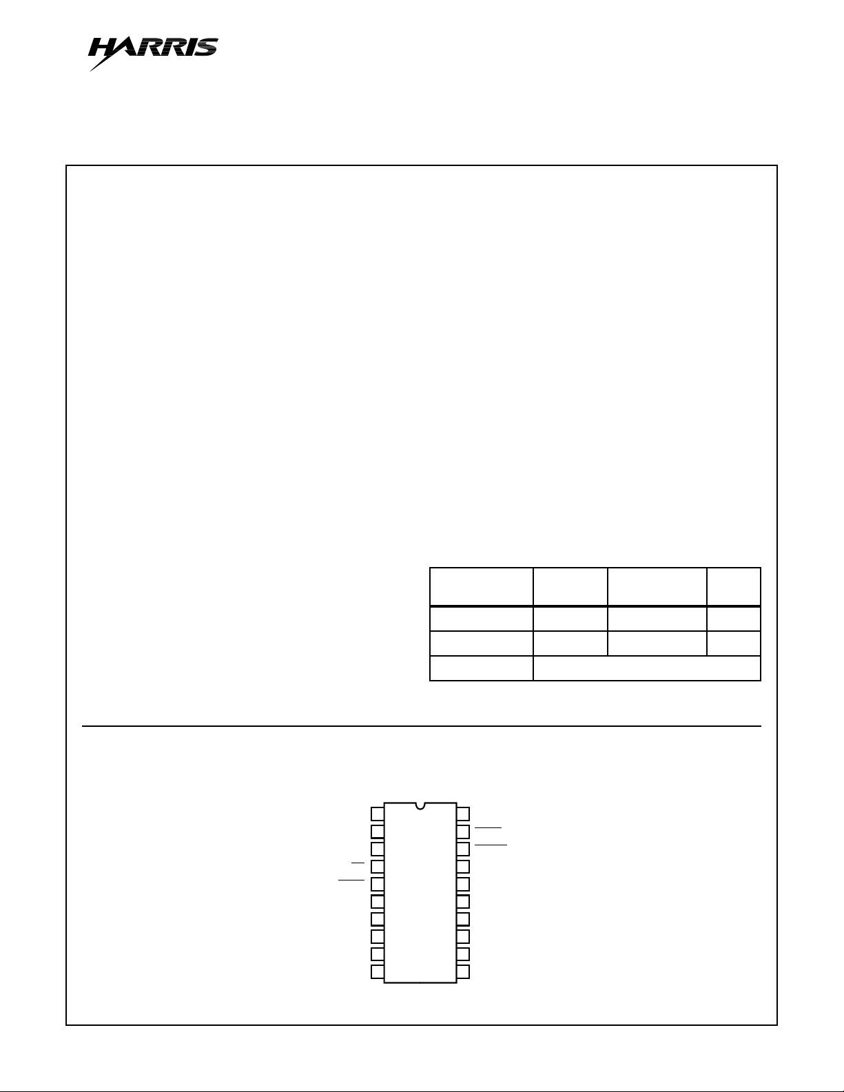
Pinout
HI7190
(PDIP, SOIC)
TOP VIEW
1
SCLK
SDO
2
SDIO
3
4
CS
5
DRDY
6
DGND
7
AV
SS
8
V
RLO
9
V
RHI
10
V
CM
CAUTION: These devices are sensitive to electrostatic discharge. Users should follow proper IC Handling Procedures.
Copyright
© Harris Corporation 1998
1871
20
19
18
17
16
15
14
13
12
11
MODE
SYNC
RESET
OSC
1
OSC
2
DV
DD
AGND
AV
DD
V
INHI
V
INLO
File Number 3612.5
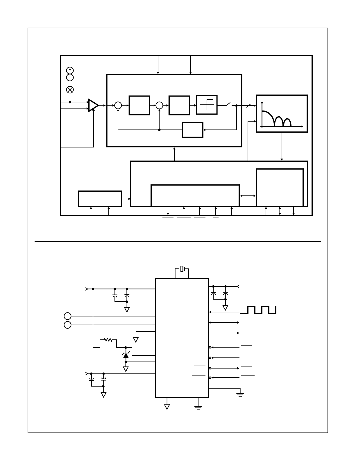
Functional Block Diagram
HI7190
V
V
INHI
INLO
V
CM
AV
DD
TRANSDUCER
BURN-OUT
CURRENT
PGIA
CLOCK
GENERATOR
V
RHI
REFERENCE
INPUTS
V
RLO
∑ − ∆
MODULATOR
∑
∫∫
∑
1-BIT
D/A
CONTROL AND SERIAL INTERFACE UNIT
CONTROL REGISTER
DIGITAL FILTER
1
SERIAL INTERFACE
UNIT
OSC1OSC
2
Typical Application Schematic
INPUT
INPUT
+5V
+
-
REFERENCE
-5V
0.1µF
R
+
+
0.1uF
1
+2.5V
4.7µF
4.7µF
DRDY RESET SYNC CS MODE S
10MHz
17 16
AV
V
INHI
V
INLO
V
CM
V
RHI
V
RLO
AV
AGND
DD
SS
OSC1OSC
14 6
13
12
11
10
9
8
7
2
RESET
MODE
DGND
DV
DD
SCLK
SDIO
SDO
SYNC
CS
DRDY
15
0.1µF
1
3
2
19
4
5
18
20
+
4.7µF
+5V
DATA I/O
DATA OUT
SYNC
CS
DRDY
RESET
CLK
SDIO SDO
1872

HI7190
Absolute Maximum Ratings Thermal Information
Supply Voltage
AVDD to AGND . . . . . . . . . . . . . . . . . . . . . . . . . . . . . . . . . . .+5.5V
AVSS to AGND . . . . . . . . . . . . . . . . . . . . . . . . . . . . . . . . . . . -5.5V
DVDD to DGND. . . . . . . . . . . . . . . . . . . . . . . . . . . . . . . . . . +5.5V
DGND to AGND . . . . . . . . . . . . . . . . . . . . . . . . . . . . . . . . . ±0.3V
Analog Input Pins . . . . . . . . . . . . . . . . . . . . . . . . . . . . AVSS to AV
Digital Input, Output and I/O Pins. . . . . . . . . . . . . . . DGND to DV
ESD Tolerance (No Damage)
Human Body Model . . . . . . . . . . . . . . . . . . . . . . . . . . . . . . . 500V
Machine Model . . . . . . . . . . . . . . . . . . . . . . . . . . . . . . . . . . +100V
Charged Device Model . . . . . . . . . . . . . . . . . . . . . . . . . . . . 1000V
Operating Conditions
Temperature Range . . . . . . . . . . . . . . . . . . . . . . . . . . -40oC to 85oC
CAUTION: Stresses above those listed in “Absolute Maximum Ratings” may cause permanent damage to the device. This is a stress only rating and operation
of the device at these or any other conditions above those indicated in the operational sections of this specification is not implied.
Thermal Resistance (Typical, Note 1) θJA (oC/W)
PDIP Package. . . . . . . . . . . . . . . . . . . . . . . . . . . . . 125
SOIC Package. . . . . . . . . . . . . . . . . . . . . . . . . . . . . 100
Maximum Junction Temperature
Plastic Packages. . . . . . . . . . . . . . . . . . . . . . . . . . . . . . . . .150oC
DD
Maximum Storage Temperature Range . . . . . . . . . .-65oC to 150oC
DD
Maximum Lead Temperature (Soldering, 10s) . . . . . . . . . . . . 300oC
(SOIC - Lead Tips Only)
Electrical Specifications AV
= +5V, AVSS = -5V, DVDD = +5V, V
DD
= +2.5V, V
RHI
= AGND = 0V, VCM = AGND,
RLO
PGIA Gain = 1, OSCIN = 10MHz, Bipolar Input Range Selected, fN = 10Hz
PARAMETER TEST CONDITIONS MIN TYP MAX UNITS
SYSTEM PERFORMANCE
Integral Non-Linearity, INL End Point Line Method (Notes 3, 5, 6) - ±0.0007 ±0.0015 %FS
Differential Non-Linearity (Note 2) No Missing codes to 22-Bits LSB
Offset Error, V
OS
Offset Error Drift V
Full Scale Error, FSE V
Noise, e
N
Common Mode Rejection Ratio, CMRR V
See Table 1 - -- -
INHI
INHI
= V
- V
(Notes 3, 8) - 1 - µV/oC
INLO
= +2.5V (Notes 3, 5, 8, 10) - - - -
INLO
See Table 1 - - - -
CM
= 0V, V
INHI
= V
from -2V to +2V -70 - dB
INLO
Normal Mode 50Hz Rejection Filter Notch = 10Hz, 25Hz, 50Hz (Note 2) -120 - - dB
Normal Mode 60Hz Rejection Filter Notch = 10Hz, 30Hz, 60Hz (Note 2) -120 - - dB
Step Response Settling Time - 2 4 Conversions
ANALOG INPUTS
Input Voltage Range Unipolar Mode (Note 9) 0 - V
Input Voltage Range Bipolar Mode (Note 9) - V
Common Mode Input Range (Note 2) AV
Input Leakage Current, I
Input Capacitance, C
Reference Voltage Range, V
(V
= V
RHI
- V
REF
RLO
IN
IN
REF
)
Transducer Burn-Out Current, I
VIN = AVDD (Note 2) - - 1.0 nA
BO
REF
SS
- 5.0 -pF
2.5 - 5 V
- 200 - nA
-V
-AVDDV
REF
REF
V
V
CALIBRATION LIMITS
Positive Full Scale Calibration Limit - - 1.2(V
Negative Full Scale Calibration Limit - - 1.2(V
Offset Calibration Limit - - 1.2(V
Input Span 0.2(V
/Gain) - 2.4(V
REF
/Gain) -
REF
/Gain) -
REF
/Gain) -
REF
/Gain) -
REF
DIGITAL INPUTS
Input Logic High Voltage, V
Input Logic Low Voltage, V
Input Logic Current, I
I
IH
IL
(Note 11) 2.0 - - V
- - 0.8 V
VIN = 0V, +5V - 1.0 10 µA
1873
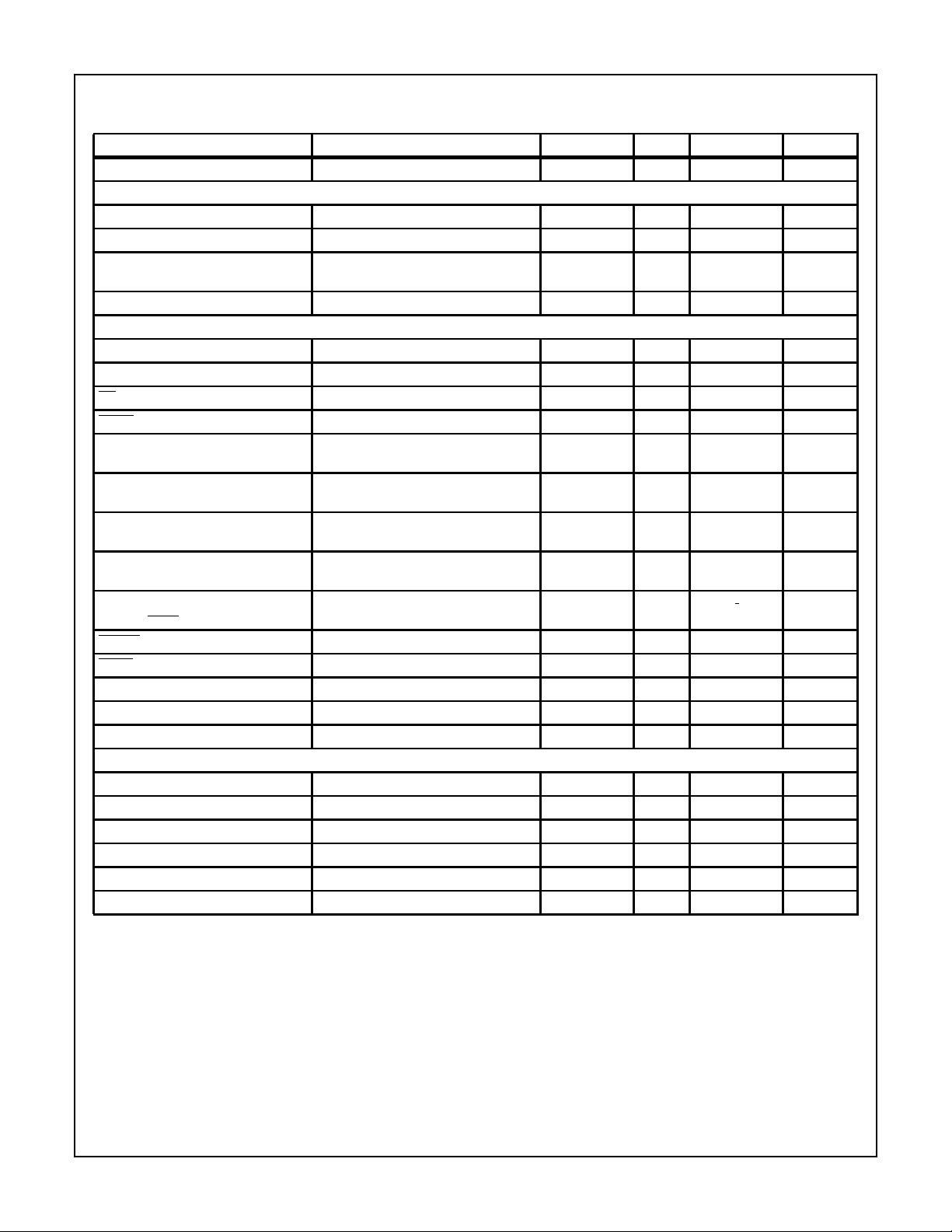
HI7190
Electrical Specifications AV
= +5V, AVSS = -5V, DVDD = +5V, V
DD
= +2.5V, V
RHI
= AGND = 0V, VCM = AGND,
RLO
PGIA Gain = 1, OSCIN = 10MHz, Bipolar Input Range Selected, fN = 10Hz (Continued)
PARAMETER TEST CONDITIONS MIN TYP MAX UNITS
Input Capacitance, C
IN
VIN = 0V - 5.0 - pF
DIGITAL OUTPUTS
Output Logic High Voltage, V
Output Logic Low Voltage, V
OH
OL
Output Three-State Leakage Current,
I
OZ
Digital Output Capacitance, C
OUT
I
= -100µA (Note 7) 2.4 - - V
OUT
I
= 3mA (Note 7) - - 0.4 V
OUT
V
= 0V, +5V (Note 7) -10 1 10 µA
OUT
-10- pF
TIMING CHARACTERISTICS
SCLK Minimum Cycle Time, t
SCLK Minimum Pulse Width, t
CS to SCLK Precharge Time, t
SCLK
SCLKPW
PRE
200 - - ns
50 - - ns
50 - - ns
DRDY Minimum High Pulse Width (Notes 2, 7) 500 - - ns
Data Setup to SCLK Rising Edge
(Write), t
DSU
Data Hold from SCLK Rising Edge
(Write), t
DHLD
Data Read Access from Instruction
Byte Write, t
ACC
Read Bit Valid from SCLK Falling Edge,
t
DV
Last Data Transfer to Data Ready
Inactive,t
DRDY
(Note 7) - - 40 ns
(Note 7) - - 40 ns
(Note 7) - 35 -ns
50 - - ns
0-- ns
RESET Low Pulse Width (Note 2) 100 - - ns
SYNC Low Pulse Width (Note 2) 100 - - ns
Oscillator Clock Frequency (Note 2) 0.1 - 10 MHz
Output Rise/Fall Time (Note 2) - - 30 ns
Input Rise/Fall Time (Note 2) - - 1 µs
POWER SUPPLY CHARACTERISTICS
IAV
DD
IAV
SS
IDV
DD
Power Dissipation, Active PD
Power Dissipation, Standby PD
SCLK = 4MHz - - 3.0 mA
A
SB = ‘0’ - 15 30 mW
SB = ‘1’ - 5 - mW
S
- - 1.5 mA
- - 1.5 mA
PSRR (Note 3) - -70 - dB
NOTES:
1. θJA is measured with the component mounted on an evaluation PC board in free air.
2. Parameter guaranteed by design or characterization, not production tested.
3. Applies to both bipolar and unipolar input ranges.
4. These errors can be removed by re-calibrating at the desired operating temperature.
5. Applies after system calibration.
6. Fully differential input signal source is used.
7. See Load Test Circuit, Figure 10, R1 = 10kΩ, CL = 50pF.
8. 1 LSB = 298nV at 24 bits for a Full Scale Range of 5V.
9. V
= V
RHI
- V
RLO
REF
10. These errors are on the order of the output noise shown in Table 1.
11. All inputs except OSC1. The OSC1 input VIH is 3.5V minimum.
1874

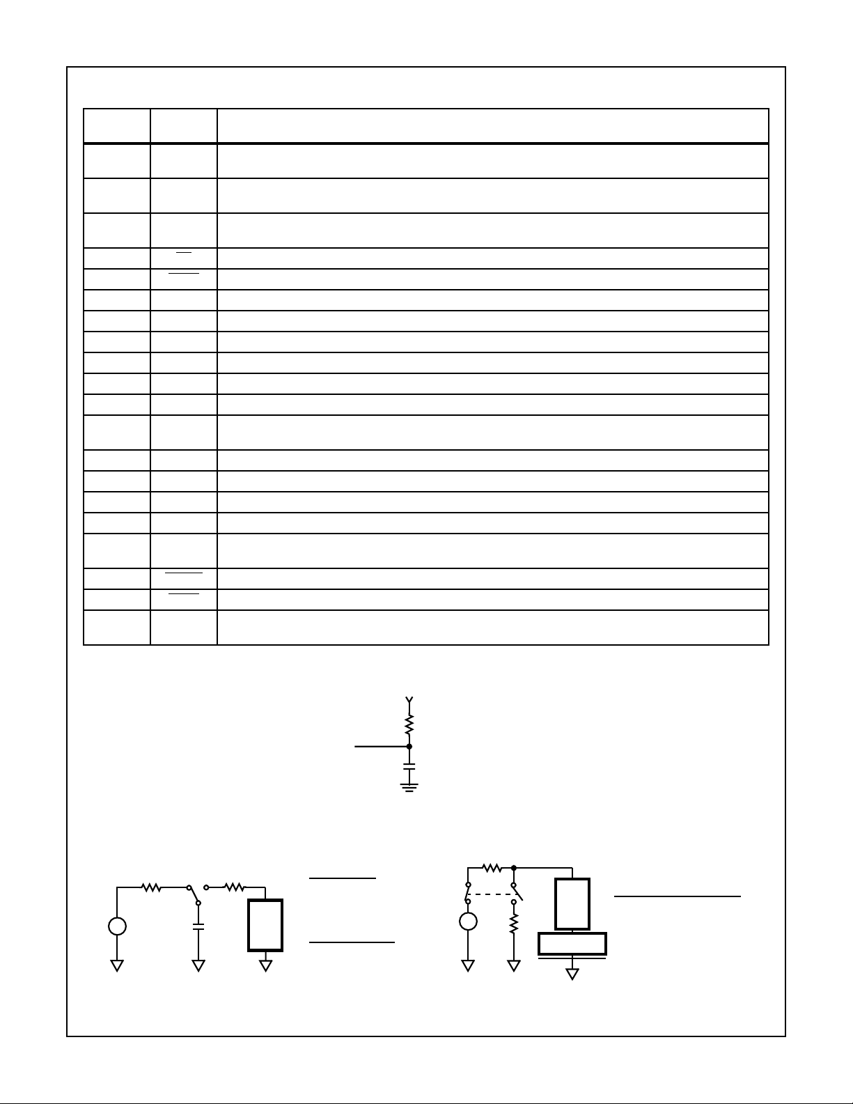
Timing Diagrams
CS
SCLK
SDIO
HI7190
t
t
DHLD
SCLK
t
SCLKPW
t
PRE
t
DSU
1ST BIT 2ND BIT
t
SCLKPW
FIGURE 1. DATA WRITE TO HI7190
SCLK
SDIO
SDO
DRDY
CS
CS
t
ACC
1ST BIT 2ND BIT
t
DV
FIGURE 2. DATA READ FROM HI7190
t
DRDY
SCLK
SDIO
87651
FIGURE 3. DATA READ FROM HI7190
1875
HI7190
Pin Descriptions
20 LEAD
DIP, SOIC PIN NAME DESCRIPTION
1 SCLK Serial Interface Clock. Synchronizes serial data transfers. Data is input on the rising edge and output on the
falling edge.
2 SDO Serial Data OUT. Serial data is read from this line when using a 3-wire serial protocol such as the
Motorola Serial Peripheral Interface.
3 SDIO Serial Data IN or OUT. This line is bidirectional programmable and interfaces directly to the Intel Standard Serial
Interface using a 2-wire serial protocol.
4 CS Chip Select Input. Used to select the HI7190 for a serial data transfer cycle. This line can be tied to DGND.
5 DRDY An Active Low Interrupt indicating that a new data word is available for reading.
6 DGND Digital Supply Ground.
7AVSSNegative Analog Power Supply (-5V).
8V
RLO
9V
10 V
11 V
12 V
INLO
INHI
13 AV
14 AGND Analog Supply Ground.
15 DV
16 OSC2Used to connect a crystal source between OSC1 and OSC2. Leave open otherwise.
17 OSC1Oscillator Clock Input for the device. A crystal connected between OSC1 and OSC2will provide a clock to the
18 RESET Active Low Reset Pin. Used to initialize the HI7190 registers, filter and state machines.
19 SYNC Active Low Sync Input. Used to control the synchronization of a number of HI7190s . A logic ‘0’ initializes the converter .
20 MODE Mode Pin. Used to select between Synchronous Self Clocking (Mode = 1) or Synchronous External Clocking
External Reference Input. Should be negative referenced to V
External Reference Input. Should be positive referenced to V
RHI
Common Mode Input. Should be set to halfway between AVDD and AVSS.
CM
RHI
RLO
.
.
Analog Input LO. Negative input of the PGIA.
Analog Input HI. Positive input of the PGIA. The V
input is connected to a current source that can be used to check
INHI
the condition of an external transducer. This current source is controlled via the Control Register.
Positive Analog Power Supply (+5V).
DD
Positive Digital Supply (+5V).
DD
device, or an external oscillator can drive OSC1. The oscillator frequency should be 10MHz (Typ).
(Mode = 0) for the Serial Port.
Load Test Circuit
ESD Test Circuits
R
1
±
V
C
R
2
DUT
ESD
FIGURE 5A.
DUT
HUMAN BODY
= 100pF
C
ESD
R1 = 10MΩ
R2 = 1.5kΩ
MACHINE MODEL
C
= 200pF
ESD
R1 = 10MΩ
= 0Ω
R
2
V
1
R
1
CL (INCLUDES STRAY
CAPACITANCE)
FIGURE 4.
±
V
R
1
DUT
R
2
DIELECTRIC
CHARGED DEVICE MODEL
R1 = 1GΩ
R2 = 1Ω
FIGURE 5B.
1876
TABLE 1. NOISE PERFORMANCE WITH INPUTS CONNECTED TO ANALOG GROUND
P-P NOISE
HERTZ SNR ENOB
GAIN = 1
10 132.3 21.7 9.8 1.5
25 129.5 21.2 13.6 2.1
30 127.7 20.9 16.6 2.5
50 126.3 20.7 19.5 3.0
60 125.6 20.6 21.2 3.2
100 122.4 20.0 30.7 4.6
250 107.7 17.6 166.7 25.3
500 98.1 16.0 505.3 76.6
1000 85.7 13.9 2101.8 318.5
2000 68.8 11.1 14661.6 2221.4
GAIN = 2
10 129.2 21.2 14.0 2.1
25 125.7 20.6 20.9 3.2
30 124.5 20.4 24.1 3.7
50 123.4 20.2 27.3 4.1
60 122.5 20.1 30.3 4.6
100 118.1 19.3 50.0 7.6
250 106.1 17.3 199.5 30.2
500 96.9 15.8 580.1 87.9
1000 84.4 13.7 2435.6 369.0
2000 67.8 11.0 16469.7 2495.4
GAIN = 4
10 125.9 20.6 20.5 3.1
25 123.1 20.1 28.4 4.3
30 121.8 19.9 32.8 5.0
50 119.9 19.6 40.9 6.2
60 119.9 19.6 40.9 6.2
100 116.1 19.0 63.2 9.6
250 105.7 17.3 209.7 31.8
500 96.6 15.8 597.8 90.6
1000 84.3 13.7 2469.5 374.2
2000 68.2 11.0 15656.1 2372.1
GAIN = 8
10 124.7 20.4 23.4 3.5
25 120.6 19.7 37.8 5.7
30 119.2 19.5 44.3 6.7
50 117.5 19.2 53.8 8.2
60 116.8 19.1 58.6 8.9
100 112.1 18.3 100.0 15.2
250 101.4 16.5 345.2 52.3
500 95.3 15.5 691.1 104.7
1000 83.1 13.5 2838.6 430.1
2000 68.3 11.1 15494.7 2347.7
(µV)
RMS NOISE
(µV)
HI7190
GAIN = 16
GAIN = 32
GAIN = 64
GAIN = 128
P-P NOISE
HERTZ SNR ENOB
10 120.1 19.7 39.8 6.0
25 114.8 18.8 73.4 11.1
30 113.5 18.6 85.1 12.9
50 111.0 18.1 114.4 17.3
60 109.6 17.9 134.0 20.3
100 105.5 17.2 214.8 32.5
250 95.2 15.5 699.1 105.9
500 89.1 14.5 1417.7 214.8
1000 83.5 13.6 2686.0 407.0
2000 62.6 10.1 30110.0 4562.1
10 113.2 18.5 88.8 13.5
25 109.0 17.8 142.7 21.6
30 108.2 17.7 157.4 23.8
50 104.7 17.1 235.8 35.7
60 105.0 17.1 227.8 34.5
100 102.3 16.7 310.5 47.0
250 93.4 15.2 861.1 130.5
500 87.1 14.2 1782.7 270.1
1000 78.2 12.7 4990.4 756.1
2000 57.0 9.2 57311.1 8683.5
10 106.7 17.4 186.2 28.2
25 102.9 16.8 288.4 43.7
30 101.9 16.6 325.8 49.4
50 98.5 16.1 479.8 72.7
60 98.9 16.1 459.8 69.7
100 96.3 15.7 620.2 94.0
250 85.5 13.9 2133.5 323.3
500 78.1 12.7 5025.0 761.4
1000 66.7 10.8 18693.5 2832.3
2000 50.5 8.1 120163.0 18206.5
10 101.1 16.5 356.5 54.0
25 96.0 15.7 638.3 96.7
30 95.2 15.5 704.8 106.8
50 93.2 15.2 882.2 133.7
60 92.2 15.0 996.7 151.0
100 91.4 14.9 1086.6 164.6
250 79.4 12.9 4346.4 658.5
500 71.8 11.6 10439.2 1581.7
1000 60.1 9.7 39923.0 6048.9
2000 44.8 7.1 233238.2 35339.1
(µV)
RMS NOISE
(µV)
1877

HI7190
Definitions
Integral Non-Linearity, INL, is the maximum deviation of
any digital code from a straight line passing through the endpoints of the transfer function. The endpoints of the transfer
function are zero scale (a point 0.5 LSB below the first code
transition 000...000 and 000...001) and full scale (a point 0.5
LSB above the last code transition 111...110 to 111...111).
Differential Non-Linearity, DNL, is the deviation from the
actual difference between midpoints and the ideal difference
between midpoints (1 LSB) for adjacent codes. If this difference is equal to or more negative than 1 LSB, a code will be
missed.
Offset Error , V
from the ideal input voltage (V
be calibrated to the order of the noise level sho wn in Table 1.
Full Scale Error, FSE, is the deviation of the last code
transition from the ideal input full scale voltage
(V
-+V
IN
REF
to the order of the noise level shown in Table 1.
Input Span, defines the minimum and maximum input
voltages the device can handle while still calibrating properly
for gain.
Noise, e
, Table 1 shows the peak-to-peak and RMS noise
N
for typical notch and -3dB frequencies. The device programming was for bipolar input with a V
the input range is 5V. The analysis was performed on 100
conversions with the peak-to-peak output noise being the
difference between the maximum and minimum readings
over a rolling 10 conversion window . The equation to convert
the peak-to-peak noise data to ENOB is:
ENOB = Log
where: V
FS
CF = 6.6 (Imperical Crest Factor)
The noise from the part comes from two sources, the
quantization noise from the analog-to-digital conversion process and device noise. Device noise (or Wideband Noise) is
independent of gain and essentially flat across the frequency
spectrum. Quantization noise is ratiometric to input full scale
(and hence gain) and its frequency response is shaped by
the modulator.
Looking at Table 1, as the cutoff frequency increases the
output noise increases. This is due to more of the
quantization noise of the part coming through to the output
and, hence, the output noise increases with increasing 3dB frequencies. For the lower notch settings, the output
noise is dominated by the device noise and, hence, altering
the gain has little effect on the output noise. At higher notch
frequencies, the quantization noise dominates the output
noise and, in this case, the output noise tends to decrease
with increasing gain.
Since the output noise comes from two sources, the effectiv e
resolution of the device (i.e., the ratio of the input full scale to
the output RMS noise) does not remain constant with
increasing gain or with increasing bandwidth. It is possible to
, is the deviation of the first code transition
OS
- 0.5 LSB). This error can
IN
/Gain - 1.5 LSB). This error can be calibrated
of +2.5V. This implies
REF
(VFS / V
2
= 5V, V
NRMS
NRMS
= V
)
NP-P
/ CF and
do post-filtering (such as brick wall filtering) on the data to
improve the ov erall resolution for a given -3dB frequency and
also to further reduce the output noise.
Circuit Description
The HI7190 is a monolithic, sigma delta A/D converter which
operates from ±5V supplies and is intended for
measurement of wide dynamic range, low frequency signals.
It contains a Programmable Gain Instrumentation Amplifier
(PGIA), sigma delta ADC, digital filter, bidirectional serial
port (compatible with many industry standard protocols),
clock oscillator, and an on-chip controller.
The signal and reference inputs are fully differential for
maximum flexibility and performance. Normally V
V
are tied to +2.5V and AGND respectively. This allows
RLO
for input ranges of 2.5V and 5V when operating in the unipolar and bipolar modes respectively (assuming the PGIA is
configured for a gain of 1). The internal PGIA provides input
gains from 1 to 128 and eliminates the need for external preamplifiers. This means the device will convert signals ranging from 0V to +20mV and 0V to +2.5V when operating in
the unipolar mode or signals in the range of ±20mV to ±2.5V
when operating in the bipolar mode.
The input signal is continuously sampled at the input to the
HI7190 at a clock rate set by the oscillator frequency and the
selected gain. This signal then passes through the sigma
delta modulator (which includes the PGIA) and emerges as
a pulse train whose code density contains the analog signal
information. The output of the modulator is fed into the sinc
digital low pass filter. The filter output passes into the
calibration block where offset and gain errors are removed.
The calibrated data is then coded (2’s complement, offset
binary or binary) before being stored in the Data Output
Register. The Data Output Register update rate is determined by the first notch frequency of the digital filter. This
first notch frequency is programmed into HI7190 via the
Control Register and has a range of 10Hz to 1.953kHz which
corresponds to -3dB frequencies of 2.62Hz and 512Hz
respectively.
Output data coding on the HI7190 is programmable via the
Control Register. When operating in bipolar mode, data output can be either 2’s complement or offset binary. In unipolar
mode output is binary.
The
DRDY signal is used to alert the user that new output
data is available. Converted data is read via the HI7190
serial I/O port which is compatible with most synchronous
transfer formats including both the Motorola 6805/11 series
SPI and Intel 8051 series SSR protocols. Data Integrity is
always maintained at the HI7190 output port. This means
that if a data read of conversion N is begun but not finished
before the next conversion (conversion N + 1) is complete,
the
DRDY line remains active (low) and the data being read
is not overwritten.
The HI7190 provides many calibration modes that can be
initiated at any time by writing to the Control Register. The
device can perform system calibration where external components are included with the HI7190 in the calibration loop
RHI
and
3
1878
 Loading...